Table of Contents
Advertisement
Quick Links
Advertisement
Table of Contents

Related Manuals for Advantech PCM-9388


Summary of Contents for Advantech PCM-9388
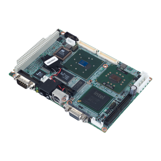
- Page 1 User Manual PCM-9388...
- Page 2 Creative is a trademark of Creative Technology LTD. CHRONTEL is a trademark of Chrontel Inc. All other product names or trademarks are properties of their respective owners. Part No. 2006938810 Edition 1 Printed in China March 2008 PCM-9388 User Manual...
-
Page 3: Product Warranty
ADVANTECH Repair Service Department. For those products which are not DOA, the return fee to an authorized ADVANTECH repair facility will be at the customers’ expense. The shipping fee for reconstructive products from ADVANTECH back to customers’ sites will be at ADVANTECH’s expense. -
Page 4: Declaration Of Conformity
Discard used batteries according to the manufacturer’s instructions. Technical Support and Assistance For more information about this and other Advantech products, please visit our web- site at: http://www.advantech.com/ http://www.advantech.com/ePlatform/ For technical support and service, please visit our support website at: http://support.advantech.com.tw/support/... -
Page 5: Packing List
Packing List Before installation, please ensure the following items have been shipped: Item Part Number 1 PCM-9388 SBC 1 Startup manual 1 Utility CD 1 Printer Port cable 1700000265 1 mini jumper pack 9689000002 1 IDE cable 1701440351 1 Audio cable... - Page 6 PCM-9388 User Manual...
-
Page 7: Table Of Contents
2.2.2 Connector Settings ..............11 Mechanical ....................14 2.3.1 Jumper and Connector Location..........14 Figure 2.1 PCM-9388 Jumper and Connector Layout (Component Side) ................. 14 Figure 2.2 PCM-9388 Jumper and Connector Layout (Solder Side) ................. 14 2.3.2 Board Dimensions............... 15 Figure 2.3 Board Dimensions (Component Side) - Page 8 4.3.4 SUSI Sample Programs.............. 39 Figure 4.1 CL................47 Chapter Extension I/O Installation ....49 PC/104 ....................50 Appendix A Assignments....... 51 Pin Assignments ..................52 Appendix B Watchdog Timer........ 73 Watchdog Timer Sample Code............... 74 PCM-9388 User Manual viii...
-
Page 9: Chapter 1 General Introduction
Chapter General Introduction This chapter gives background information on the PCM-9388 Sections include: Introduction Specifications... -
Page 10: Introduction
Introduction The PCM-9388 is a 3.5” SBC (Single Board Computer) with Intel Celeron® M on board CPU. The PCM-9388, in conjunction with Intel 852GM and ICH4 chipsets, supports proces- sors clocked up to 1.0 GHz, two USB 2.0 compatible ports, one Ethernet connector... -
Page 11: Display
Chipset (852) Memory 852GM GMCH Supports 1GB maximum memory Two 64-bit wide DDR SDRAM data channel Support DDR 200, DDR266 MHz 128-Mb, 256-Mb, 512-Mb and 1-GB DDR technology Socket: SODIMM Socket: 1. 200 pin SODIMM socket type *1 PCM-9388 User Manual... - Page 12 Supports SMBus 2.0 Specification Host interface allows CPU to communicate via SMBus 1.3.1.4 Others(chipset) PCI to ISA ITE8888G support PCI specification V.2.1 compliant Optional CLKRUN# interface support Supports full ISA compatible functions Supports ISA at 1/4 of PCI frequency PCM-9388 User Manual...
-
Page 13: Mechanical Specifications
Voltage requirement with ATX Power: +5 VDC +/- 5% +5 VDC Standby +/- 5% +12 VDC +/- 5% (For LVDS inverter power, PC/104) Voltage requirement with AT Power: +5V DC +/- 5% +12V DC +/- 5% (For LVDS inverter power, PC/104) PCM-9388 User Manual... -
Page 14: Environmental Specifications
Operating Humidity: 0% ~ 90% Relative Humidity, non-condensing 1.3.4.3 Storage Temperature Standard products: 0 ~ 60° C Storage temperature: -20 ~ 70° C 1.3.4.4 Storage Relative Humidity Standard products (0 ~ 60° C) Relative humidity: 95% @ 60° C PCM-9388 User Manual... -
Page 15: Chapter 2 H/W Installation
Chapter H/W installation This chapter explains the setup procedures of the PCM-9388 hard- ware, including mechanical draw- ings, and instructions on setting jumpers and connecting peripher- als, switches, and indicators. Be sure to read all safety precautions before you begin the installation... -
Page 16: Jumpers
PIN HEADER 2*1P 180D (M) SQUARE 2. 0mm Setting Function J3 (1-2) RS-422 J4 (1-2) RS-232 J5 (1-2) RS-485 LCD power selector Description PIN HEADER 3*1P 180D(M) 2.0 mm DIP SQUARE W/O Pb Setting Function J6 (1-2) +5 V J6 (2-3) +.3.3 V PCM-9388 User Manual... -
Page 17: Jumper Description
+5 V +3.3 V Warning! To avoid damaging the computer, always turn off the power supply before setting jumpers. Clear CMOS. Before turning on the power sup- ply, set the jumper back to 3.0 V Battery On. PCM-9388 User Manual... -
Page 18: Connectors
CN15 COM2 RS-232/RS-422/RS-485 Connector CN16 USB Connector CN17 PS2 (KB & MS) CN19 LAN Connector CN20 PC/104 SOLDER CONNECTOR CN21 Negative POWER Input CN22 LVDS LCD 40-Pin HIROSE CN23 Invert Power Connector CN24 TTL LCD 40-Pin HIROSE PCM-9388 User Manual... -
Page 19: Connector Settings
Power Connectors (CN1, CN2, CN4, CN5) Main power connector, +5 V, +12 V or 5V only PCM-9388 supports ATX and AT modes. One 4-Pin connector (CN1) supports 5 V/12 V AT power supply. Use ATX power cable (PN: 1703200201 ATX power control cable) connect CN2; it provides 5 VSB for ATX power. - Page 20 The LCD inverter is connected to CN6 via a 5-pin connector to provide +5 V/+12 V power. 2.2.2.9 COM Port Connector (CN12, CN15, J3/J4/J5) The PCM-9388 provides 2 serial ports (COM1 and COM2). One 7*2P PIN HEADER (CN15) for COM2 output; and one DB-9 connector for COM1(CN12) COM RS-232/422/485 settings (J3) COM2 can be configured to operate in RS-232, RS-422, or RS-485 mode.
- Page 21 Socket3: 32 x 2 (F) 2.5 4mm 82.34 mm x 5.01 mm x 11.45 mm p = 3.40 mm PC/104 negative voltage: One 3 x 1-pin wafer box (CN23) supports -5 V/-12 V power input for ISA devices. PCM-9388 User Manual...
-
Page 22: Mechanical
Mechanical 2.3.1 Jumper and Connector Location Figure 2.1 PCM-9388 Jumper and Connector Layout (Component Side) Figure 2.2 PCM-9388 Jumper and Connector Layout (Solder Side) PCM-9388 User Manual... -
Page 23: Board Dimensions
2.3.2 Board Dimensions Figure 2.3 Board Dimensions (Component Side) Figure 2.4 Board Dimensions (Solder Side) PCM-9388 User Manual... - Page 24 PCM-9388 User Manual...
-
Page 25: Chapter 3 Bios Operation
Chapter BIOS Operation Sections include: BIOS Introduction BIOS Setup... -
Page 26: Bios Introduction
CPUs from 386 through Pentium and AMD Geode, K7 and K8 (including multiple pro- cessor platforms), and VIA Eden C3 and C7 CPUs. You can use Advantech’s utilities to select and install features to suit your designs for customers needs. -
Page 27: Main Menu
Set Password Establish, change or disable password. Save & Exit Setup Save CMOS value settings to CMOS and exit BIOS setup. Exit Without Saving Abandon all CMOS value changes and exit BIOS setup. PCM-9388 User Manual... -
Page 28: Standard Cmos Features
The system boot will not stop for a disk error; it will stop for all other errors. All, But Disk/Key The system boot will not stop for a keyboard or disk error; it will stop for all other errors. PCM-9388 User Manual... -
Page 29: Advanced Bios Features
This item displays the total system memory size. 3.2.3 Advanced BIOS Features Blank Boot[Disabled] (* Advantech feature enhancement) This item allows system only displays blank screen during BIOS Post stage. POST Beep[Enabled] (* Advantech feature enhancement) This item allows system send out Beep sound during BIOS Post stage. - Page 30 Full Screen Logo Show[Enabled] Show full screen logo during post stage, and the Logo picture can be customized. Small Logo (EPA) Show[Enabled] Show EPA logo during system post stage. Summary Screen Show[Enabled] Show system status in Summary screen page. PCM-9388 User Manual...
-
Page 31: Advanced Chipset Features
This item enables users to set the operation speed of internal Graphic Chip FSB and DRAM, system default setting is “Auto Max 266 MHz”. System BIOS Cacheable[Enabled] This item allows the system BIOS to be cached to allow faster execution and better performance. Video BIOS Cacheable[Disabled] PCM-9388 User Manual... - Page 32 This Item enables users to set Initial display device of system boot up, system default setting is “VBIOS Default”. Panel Number [640X480] This item enables users to set the Resolution of Panel Type, system default set- ting ia “640X480”. PCM-9388 User Manual...
-
Page 33: Integrated Peripherals
This item enables users to set the Super IO device status, including enabling Floppy, COM, LPT, IR and control GPIO and Power fail status. Onboard Serial port 1 [ 3F8] This item allows user to adjust serial port 1 of address. PCM-9388 User Manual... -
Page 34: Power Management Setup
V/H SYNC+Blank This option will cause system to turn off vertical and horizontal syn- chronization ports and write blanks to the video buffer. Blank Screen This option only writes blanks to the video buffer. DPMS Initial display power management signaling. Video Off In Suspend[Yes] PCM-9388 User Manual... - Page 35 This item allows user to enable and key in Date/time to power on system Disabled Disable this function. Enabled Enable alarm function to power on system Data (of month) Alarm 1-31 Time (HH:MM:SS) Alarm (0-23) : (0-59) : 0-59) PCM-9388 User Manual...
-
Page 36: Pnp/Pci Configurations
The item is designed to solve problems caused by some non-standard VGA cards. A built-in VGA system does not need this function. INT Pin 1 ~ 8 Assignment[Auto] The interrupt request (IRQ) assigned to devices connected to the PCI interface on your system. PCM-9388 User Manual... -
Page 37: Pc Health Status
FAN 1 / FAN2 / FAN3 / FAN4 Speed [Show Only] This item displays current system FAN speed. 2.5 V / 3.3 V / 5 V / 12 V and VCore [Show Only] This item displays current CPU and system Voltage. PCM-9388 User Manual... -
Page 38: Frequency/Voltage Control
Spread Spectrum [Disabled] This item enables users to set the spread spectrum modulation. CPU Host/SRC/PCI Clock [Default] This item enables users to set the CPU Host and PCI clock by system auto- matic detection or manually PCM-9388 User Manual... -
Page 39: Load Optimized Defaults
Load Optimized Defaults loads the default system values directly from ROM, if the stored record created by the Setup program should ever become corrupted (and therefore unusable). These defaults will load automatically when you turn on the PCM-9388. PCM-9388 User Manual... -
Page 40: Set Password
Select Set Password again, and at the “Enter Password” prompt, enter the new password and press <Enter>. At the “Confirm Password” prompt, retype the new password, and press <Enter>. Select Save to CMOS and EXIT, type <Y>, then <Enter>. PCM-9388 User Manual... - Page 41 Select Set Password again, and at the “Enter Password” prompt, don’t enter anything; just press <Enter>. At the “Confirm Password” prompt, again, don’t type in anything; just press <Enter>. Select Save to CMOS and EXIT, type <Y>, then <Enter>. PCM-9388 User Manual...
-
Page 42: Save & Exit Setup
Typing "Y" will quit the BIOS Setup Utility and save user setup value to CMOS. Typing "N" will return to the BIOS Setup Utility. 3.2.13 Quit Without Saving Note! Typing "Y" will quit the BIOS Setup Utility without saving to CMOS. Typing "N" will return to the BIOS Setup Utility. PCM-9388 User Manual... -
Page 43: S/W Introduction & Installation
Chapter S/W Introduction & Installation Sections include: S/W Introduction Driver Installation SUSI Application Library... -
Page 44: S/W Introduction
S/W Introduction The mission of Advantech Embedded Software Services is to: "Enhance the quality of life with Advantech platforms and Microsoft Windows Embedded technology". We enable Windows Embedded software products on Advantech platforms to more effectively support the embedded computing community. Customers are freed from the hassle of dealing with multiple vendors (Hardware suppliers, System integrators, Embedded OS distributor) for projects. -
Page 45: Susi Application Library
The benefit of using SUSI is portability. The same set of APIs is defined for different Advantech hardware platforms. Also, the same set of APIs is implemented in different Operating Systems including Windows XP and Windows CE. -
Page 46: Susi Installation
However, due to the inaccuracy among many commercially available hardware mon- itoring chips, Advantech has developed a unique scheme for hardware monitoring - achieved by using a dedicated microprocessor with algorithms specifically designed for providing accurate, real-time and reliable data content; helping protect your sys- tem in a more reliable manner 4.3.3... -
Page 47: Susi Sample Programs
Windows CE In Windows CE, there are three ways to install the SUSI Library, you can install it manually or use Advantech CE-Builder to install the library or just copy the programs and the library onto a compact flash card. - Page 48 For a complete list of supported applications, please refer to Appendix A where the steps to test all functions of this application are described. PCM-9388 User Manual...
- Page 49 Key in the value either '0' or '1' in (R/W) Result field to write the output pin you chose above step. – Click the WRITE GPIO DATA button to write the GPIO output pin. Test Write Multiple Output Pins – Click the radio button- Multiple-Pins. PCM-9388 User Manual...
- Page 50 Key in the register offset in Register Offset field. – Key in the desired data in the Result field to write to the device. – Click the “WRITE A BYTE” button and the data will be written to the device through I2C. PCM-9388 User Manual...
- Page 51 Click the “READ SMBus DATA” button and then a word of data from the device will be shown on the Result field. Write a word – Click the radio button- Access a word. – Key in the slave device address in the Slave address field. PCM-9388 User Manual...
- Page 52 Key in all the desired data in the Result field in hexadecimal format, sepa- rated by commas, for example, 0x50, 0x60, 0x7A. – Click the “WRITE SMBus DATA” button and all of the data will be written to the device through the SMBus. PCM-9388 User Manual...
- Page 53 Move the slider up, using either the mouse or the direction keys, or click the UP button to increase the brightness. – Move the slider down, using either the mouse or the direction keys, or click the DOWN button to decrease the brightness. PCM-9388 User Manual...
- Page 54 Before the timer counts down to zero, it can be reset by clicking the REFRESH button. After clicking this button, the Timeout Countdown field will display the value of the SET TIMEOUT field. If you want to stop the watchdog timer, just click the STOP button. PCM-9388 User Manual...
-
Page 55: Figure 4.1 Cl
When the Monitor application is executed by clicking the button, hardware monitoring data values will be displayed. If certain data values are not supported by the platform, the correspondent data field will be grayed-out with a value of 0. PCM-9388 User Manual... - Page 56 PCM-9388 User Manual...
-
Page 57: Extension I/O Installation
Chapter Extension I/O Installation... -
Page 58: Pc/104
After applying force to the connector. The footprint of the module/CPU board needs to be inserted correctly. After applying force to the connector. The footprint of the module/CPU board need to be inserted correctly. PCM-9388 User Manual... -
Page 59: Appendix A Pin Assignments
Appendix Pin Assignments... -
Page 60: Pin Assignments
+12 V +5 V ATX POWER Standby Connector Description WAFER BOX 2.0 mm 3P 180D Pin name +5 VSB PSON# SMBUS Description WAFER BOX 2.0 mm 4P 180D (M) W/LOCK A2001WV2-4P Pin name SMBDAT SMBCLK +5 V PCM-9388 User Manual... - Page 61 ATX Power Button Connector Description WAFER BOX 2P 180D (M) 2.0 mm W/Lock Pin Name +5 VSB PSIN GPIO Description PIN HEADER SMD 5*2P 180D (M) 2.0 mm Pin Name +5 V GPIO4 GPIO0 GPIO5 GPIO1 GPIO6 GPIO2 GPIO7 GPIO3 PCM-9388 User Manual...
- Page 62 AUDIO Connector Description BOX HEADER SMD 5*2 180D (M) 2.0 mm Pin Name LOUT_R LIN_R LOUT_L LIN_L MIC1R MIC1L PCM-9388 User Manual...
- Page 63 IDE Connector Description BOX HEADER SMD 22*2P 180D (M) 2.0 mm IDIOT-PROOF Pin Name RST# DD10 DD11 DD12 DD13 DD14 DD15 KEYIN DMARQ DIOW# DIOR# IORDY CSEL DMACK# INTRQ PDIAG# CS0# CS1# DASP# PCM-9388 User Manual...
- Page 64 Compact Flash Description CF HEADER 50P 90D(M) 1.27 MM SMD N016@0140-004 Pin Name CS0# CD2# CD1# CS1# VS1# PCM-9388 User Manual...
- Page 65 IORD# IOWR# IREQ CSEL# VS2# RESET IORDY INPACK# REG# DSAP# POIAG# PCM-9388 User Manual...
- Page 66 HDD & PWR LED Description WAFER BOX 2.0 mm 6P 180D Pin name +5 V Power LED+ Power LED- HDD LED+ HDD LED- CN11 Description D-SUB Conn. 15P 90D (F) DIP 070242FR015S200ZU Pin Name GREEN BLUE DDAT HSYNC VSYNC DCLK PCM-9388 User Manual...
- Page 67 Description D-SUB CON. 9P 90D (M)DIP 070241MR009S200ZU SUYIN Pin Name DCD# DTR# DSR# RTS# CTS# CN13 LPT Connector Description BOX HEADER SMD 13*2P 2.0 mm Pin name Pin name STROBE# AUTOFEED# ERROR# INIT# SLCTIN# ACK# BUSY SLCT PCM-9388 User Manual...
- Page 68 Description WAFER BOX 2.0 mm 5P 180D Pin name +5 V Reserved IRRX IRTX CN15 COM2 RS232/RS422/RS485 Connector Description BOX HEADER SMD 7*2P 180D (M) 2.0 mm Pin Name DCD# RTS# CTS# DTR# 485/422TX+ 485/422TX- 422RX+ 422RX- PCM-9388 User Manual...
- Page 69 PIN HEADER 5*2P 180D (M) 2.0 mm SMD IDIOT-PROOF Pin name +5 V +5 V A_D- B_D- A_D+ B_D- CN17 Description MINIDIN 6P 90D (F) D Short body W/Shielding WO/Pb Pin Name KBDAT MSDAT +5 V KBCLK MSCLK PCM-9388 User Manual...
- Page 70 CN19 LAN Connector Description PHONE JACK RJ45 8P 90D (F) DIP 677-088-D06 Pin name CN20 PC104 Description Pin Name IOCHCK IOCHRDY SA19 SA18 SA17 SA16 SA15 SA14 SA13 SA12 SA11 SA10 PCM-9388 User Manual...
- Page 71 RSTDRV +5 V IRQ9 -5 V DRQ2 -12 V 0WS# +12 V SMEMW# SMEMR# IOW# IOR# DACK3# DRQ3 DACK1# DRQ1 REFRESH# SYSCLK IRQ7 IRQ6 IRQ5 IRQ4 IRQ3 DACK2# ALE# BHE# LA23 LA22 LA21 LA20 LA19 LA18 PCM-9388 User Manual...
- Page 72 LA17 MEMR# MEMW# SD10 SD11 SD12 SD13 SD14 SD15 MEMCS16# IOCS16# IRQ10 IRQ11 IRQ12 IRQ15 IRQ14 DACK0# DRQ0 DACK5# DRQ5 DACK6# DRQ6 DACK7# DRQ7 +5 V MASTER# PCM-9388 User Manual...
- Page 73 +5 V or +3.3 V +5 V or +3.3 V +5 V or +3.3 V LVDS0_D0- LVDS1_D0- LVDS0_D0+ LVDS1_D0+ LVDS0_D1- LVDS1_D1- LVDS0_D1+ LVDS1_D1+ LVDS0_D2- LVDS1_D2- LVDS0_D2+ LVDS1_D2+ LVDS0_CLK- LVDS1_CLK- LVDS0_CLK+ LVDS1_CLK+ DDC_CLK DDC_DATA LVDS0_D3- LVDS1_D3- LVDS0_D3+ LVDS1_D3+ PCM-9388 User Manual...
- Page 74 CN23 Invert Power Connector Description WAFER BOX 2.0 mm 5P 180D Pin name +12 V ENABKL +5 V PCM-9388 User Manual...
- Page 75 PD5 (B3) PD6 (B4) PD7 (B5) PD10 (G0) PD11 (G1) PD12 (G2) PD13 (G3) PD14 (G4) PD15 (G5) PD18 (R0) PD19 (R1) PD20 (R2) PD21 (R3) PD22 (R4) PD23 (R5) SHFCLK FLM (V-SYNC) M/ (DE) LP (H-SYNC) ENVEE PCM-9388 User Manual...
- Page 76 *SODIMM200P DDR RVS. 0.6 mm H=5.2 90D 0-1473006-1 Pin Name VREF VREF +2.5 V +2.5 V DQS0 +2.5 V +2.5 V DQ12 DQ13 DQS1 DQ11 DQ14 DQ10 DQ15 +2.5 V +2.5 V +2.5 V CK0# DQ17 DQ21 DQ16 PCM-9388 User Manual...
- Page 77 DQ20 +2.5 V +2.5 V DQS2 DQ18 DQ23 DQ19 DQ22 DQ25 DQ28 +2.5 V +2.5 V DQ29 DQ24 DQS3 DQ26 DQ30 DQ31 DQ27 +2.5 V +2.5 V +2. 5V +2.5 V PCM-9388 User Manual...
- Page 78 +2.5 V +2.5 V +2.5 V CKE1 CKE0 +2.5 V +2.5 V RAS# CAS# DQ32 DQ36 DQ33 DQ37 +2.5 V +2.5 V DQS4 DQ38 DQ39 DQ34 PCM-9388 User Manual...
- Page 79 DQ44 DQ41 DQS5 DQ43 DQ46 DQ42 DQ47 +2.5 V +2.5 V +2.5 V CK1# DQ50 DQ52 DQ54 DQ49 +2.5 V +2.5 V DQS6 DQ48 DQ53 DQ51 DQ55 DQ56 DQ60 +2.5 V +2.5 V DQ57 DQ61 DQS7 DQ63 PCM-9388 User Manual...
- Page 80 DQ58 DQ59 DQ62 +2.5 V +2.5 V +2.5 V PCM-9388 User Manual...
-
Page 81: Appendix B Watchdog Timer
Appendix Watchdog Timer... -
Page 82: Watchdog Timer Sample Code
Watchdog Timer Sample Code NEWIODELAY MACRO 0ebh,al ENDM .MODEL small,c .486p .dosseg .stack .const Superio_Config_Port .data .code .startup call Superio_Enter_Config ;unlock superio al,10 ;set 10 seconds call Set_WDT ;Watch_Dog_Setting call Superio_Exit_Config ;lock superio .exit ================================== PCM-9388 User Manual... - Page 83 ;Input : AL - WDT timer ================================== ============================[] public Set_WDT Set_WDT proc near pusha push cl,8 ;set to device 8 call Set_Logic_Device cl,0f5h ;get and set WDT counter mode to second call Superio_Get_Reg al, not call Superio_Set_Reg cl,0f6h PCM-9388 User Manual...
- Page 84 ;set WDT Timer call Superio_Set_Reg cl,0f7h ;Disable Watchdog timer resets by the mouse or keyboard interrupts al,al call Superio_Set_Reg cl,30h ;set device active al,1 call Superio_Set_Reg popa Set_WDT Endp ================================== ============================[] ;Input : CL - logic device to set PCM-9388 User Manual...
- Page 85 Set_Logic_Device Set_Logic_Device proc near push push xchg al,cl cl,07h call Superio_Set_Reg Set_Logic_Device Endp ================================== ============================[] ;Input : CL - register index ;Output : AL - Value read ================================== ============================[] public Superio_Get_Reg Superio_Get_Reg proc Near al, cl PCM-9388 User Manual...
- Page 86 NEWIODELAY al, dx NEWIODELAY Superio_Get_Reg endp ================================== ============================[] ;Input : CL - register index AL - Value to write ================================== ============================[] public Superio_Set_Reg Superio_Set_Reg proc near push Superio_Config_Port al,cl dx,al NEWIODELAY dx,al NEWIODELAY Superio_Set_Reg endp PCM-9388 User Manual...
- Page 87 Superio_Enter_Config Superio_Enter_Config Proc Near Superio_Config_Port al, 087h dx, al dx, al Superio_Enter_Config Endp public Superio_Exit_Config Superio_Exit_Config Proc Near Superio_Config_Port al, 0AAh dx, al Superio_Exit_Config Endp PCM-9388 User Manual...
- Page 88 No part of this publication may be reproduced in any form or by any means, electronic, photocopying, recording or otherwise, without prior written permis- sion of the publisher. All brand and product names are trademarks or registered trademarks of their respective companies. © Advantech Co., Ltd. 2008...
Need help?
Do you have a question about the PCM-9388 and is the answer not in the manual?
Questions and answers