Table of Contents
Advertisement
Quick Links
Advertisement
Table of Contents

Subscribe to Our Youtube Channel
Related Manuals for EUROCOM TN120T


Summary of Contents for EUROCOM TN120T
- Page 3 Preface Notebook Computer TN120T Service Manual...
- Page 4 Preface Notice The company reserves the right to revise this publication or to change its contents without notice. Information contained herein is for reference only and does not constitute a commitment on the part of the manufacturer or any subsequent ven- dor.
- Page 5 Preface About this Manual This manual is intended for service personnel who have completed sufficient training to undertake the maintenance and inspection of personal computers. It is organized to allow you to look up basic information for servicing and/or upgrading components of the TN120T series notebook PC.
- Page 6 Preface IMPORTANT SAFETY INSTRUCTIONS Follow basic safety precautions, including those listed below, to reduce the risk of fire, electric shock and injury to per- sons when using any electrical equipment: 1. Do not use this product near water, for example near a bath tub, wash bowl, kitchen sink or laundry tub, in a wet basement or near a swimming pool.
-
Page 7: Instructions For Care And Operation
Preface Instructions for Care and Operation The notebook computer is quite rugged, but it can be damaged. To prevent this, follow these suggestions: Don’t drop it, or expose it to shock. If the computer falls, the case and the components could be damaged. Do not expose the computer Do not place it on an unstable Do not place anything heavy... -
Page 8: Power Safety
Preface Avoid interference. Keep the computer away from high capacity transformers, electric motors, and other strong mag- netic fields. These can hinder proper performance and damage your data. Take care when using peripheral devices. Use only approved brands of Unplug the power cord before peripherals. -
Page 9: Battery Precautions
Preface Battery Precautions • Only use batteries designed for this computer. The wrong battery type may explode, leak or damage the computer. • Do not continue to use a battery that has been dropped, or that appears damaged (e.g. bent or twisted) in any way. Even if the computer continues to work with a damaged battery in place, it may cause circuit damage, which may possibly result in fire. - Page 10 Preface Related Documents You may also need to consult the following manual for additional information: User’s Manual on CD This describes the notebook PC’s features and the procedures for operating the computer and its ROM-based setup pro- gram. It also describes the installation and operation of the utility programs provided with the notebook PC. VIII...
-
Page 11: Table Of Contents
Preface Contents Introduction ..........1-1 Bottom (TN120T) ................A-4 LCD (TN120T) ................A-5 Overview ..................1-1 DVD-Super Multi (TN120T) ............A-6 System Specifications ..............1-2 HDD (TN120T) ................A-7 External Locator - Top View with LCD Panel Open ......1-6 Schematic Diagrams......... B-1 External Locator - Front & Rear Views ..........1-7 External Locator - Right &... - Page 12 Preface POWER VDD3/VDD5 ..............B-27 POWER 1.05VS/1.5V/3.3V/5V ........... B-28 POWER 1.8V/0.9VSM ..............B-29 CPU VCORE ................B-30 DC-IN, CHARGER ..............B-31 Multi Board, PCIE LAN RTL8111DL ........B-32 Multi Board, LED, Docking, USB ..........B-33 Multi Board, 3G, MDC, RJ11 ............B-34 FPT ExBoard FINGERPRINT .............
-
Page 13: Introduction
Introduction Chapter 1: Introduction Overview This manual covers the information you need to service or upgrade the TN120T series notebook computer. Information about operating the computer (e.g. getting started, and the Setup utility) is in the User’s Manual. Information about driv- ers (e.g. -
Page 14: System Specifications
Introduction System Specifications Latest Specification Information The specifications listed in this Appendix are correct at the time of going to press. Certain items (particularly processor types/speeds and CD/DVD device types) may be changed, delayed or updated due to the manufacturer's release schedule. Check with your service center for details. - Page 15 Introduction Feature Specification Memory Two 200 Pin SO-DIMM Sockets Supporting DDRII (DDR2) 667/ 800 MHz 64-bit Wide DDRII (DDR2) Data Channel Memory Expandable up to 4GB (512/ 1024/ 2048 MB DDRII Modules) Supports Dual Channel DDRII (DDR2) SDRAM 2GB OR 4GB Intel® Turbo Memory Module (Option) Video Adapter Intel GMA X4500HD Integrated Video Shared Memory Architecture - Supports up to 256MB of Video Memory (dynamically allocated from system memory...
- Page 16 Introduction Feature Specification Card Slots One ExpressCard/34(54) Slot One MiniCard Slot Supporting USB and PCIe Interfaces for WLAN Module Second MiniCard Slot Supporting USB and PCIe Interfaces for Intel® Turbo Memory Module OR 3.5G Module Communication 56K Plug and Play Fax Modem 10M/ 100M/ 1000M Base-TX Ethernet LAN Note: The 3.5G Wireless LAN Module Options:...
- Page 17 Introduction Feature Specification Optional Optical Drive Module Options: Bluetooth V2.1 + EDR (Enhanced Data Rate) Module Super Multi Drive Module (Factory Option) Note: The 3.5G Blu-ray Combo Drive Module Intel Turbo Blu-ray Writer Drive Module 2GB OR 4GB Intel® Intel Turbo Memory (Robson) Memory Modules NAND Flash Memory Card Module...
-
Page 18: External Locator - Top View With Lcd Panel Open
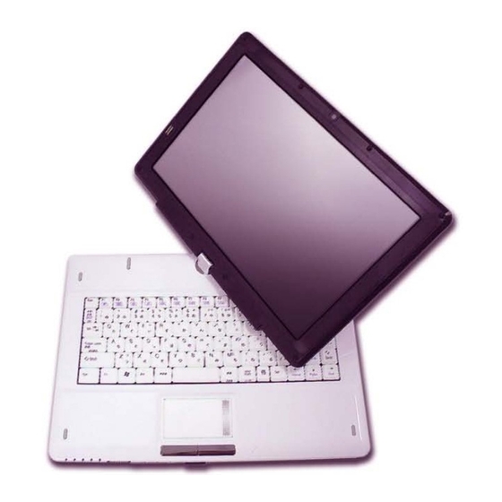
Introduction External Locator - Top View with LCD Panel Open Figure 1 Top View with LCD Panel Open 1. Built-In PC Camera (Optional) 2. LCD 3. Fingerprint Reader Module (Optional) 4. Menu & Screen Rotation Buttons 5. Speakers 6. Screen Hinge 7. -
Page 19: External Locator - Front & Rear Views
Introduction External Locator - Front & Rear Views Figure 2 Front View 1. LED Power & Communication Indicators 2. Power Switch 3. S/PDIF-Out Jack Front 4. Microphone-In Jack 5. Headphone-Out Jack 6. 7-in-1 Card Reader 7. Stylus Pen Holder Figure 3 Rear View 1. -
Page 20: External Locator - Right & Left Side Views
Introduction External Locator - Right & Left Side Views Figure 4 Right Side View 1. Stylus Pen Holder 2. Optical Device (for DVD Device) 3. Emergency Eject Hole 4. 1 * USB 2.0 Port Right 5. RJ-11 Phone Jack 6. RJ-45 LAN Jack Figure 5 Left Side View 1. -
Page 21: External Locator - Bottom View
Introduction External Locator - Bottom View Figure 6 Bottom View 1. Battery 2. Hard Disk Bay Cover (3.5G Module Location) 3. RAM & CPU Bay Cover 4. Vent Overheating To prevent your com- puter from overheating make sure nothing blocks the vent/fan in- takes while the com- puter is in use. -
Page 22: Mainboard Overview - Top (Key Parts)
Introduction Mainboard Overview - Top (Key Parts) Figure 7 Mainboard Top Key Parts 1. Clock Buffer 2. ITE 8512E 3. Card Reader Controller ENE MR510 1 - 10 Mainboard Overview - Top (Key Parts) -
Page 23: Mainboard Overview - Bottom (Key Parts)
Introduction Mainboard Overview - Bottom (Key Parts) Figure 8 Mainboard Bottom Key Parts 1. CPU Socket (no CPU installed) 2. Northbridge-intel GM965 3. ExpressCard Assembly 4. Southbridge-ICH8-M 5. Memory Slots DDRII So-DIMM 6. WLAN Mini Card Slot Mainboard Overview - Bottom (Key Parts) 1 - 11... -
Page 24: Mainboard Overview - Top (Connectors)
Introduction Mainboard Overview - Top (Connectors) Figure 9 Mainboard Top Connectors 1. Keyboard Cable Connector 2. Internal Microphone Cable Connector 3. Touch Pad Cable ConnectorBattery Connector 1 - 12 Mainboard Overview - Top (Connectors) -
Page 25: Mainboard Overview - Bottom (Connectors)
Introduction Mainboard Overview - Bottom (Connectors) Figure 10 Mainboard Bottom Connectors 1. Mini-IEEE 1394 Port 2. External Monitor Port 3. Battery Connector 14 13 4. Optical Device Drive Connector 5. 7-in-1 Card Reader 6. Headphone-Out Jack 7. Microphone-In Jack 8. S/PDIF-Out Jack 9. - Page 26 Introduction 1 - 14...
-
Page 27: Disassembly
Disassembly Chapter 2: Disassembly Overview This chapter provides step-by-step instructions for disassembling the TN120T series notebook’s parts and subsystems. When it comes to reassembly, reverse the procedures (unless otherwise indicated). We suggest you completely review any procedure before you take the computer apart. Procedures such as upgrading/replacing the RAM, CD device and hard disk are included in the User’s Manual but are repeated here for your convenience. -
Page 28: Maintenance Tools
Disassembly NOTE: All disassembly procedures assume that the system is turned OFF, and disconnected from any power supply (the battery is removed too). Maintenance Tools The following tools are recommended when working on the notebook PC: • M3 Philips-head screwdriver •... -
Page 29: Maintenance Precautions
Disassembly Maintenance Precautions The following precautions are a reminder. To avoid personal injury or damage to the computer while performing a re- moval and/or replacement job, take the following precautions: Power Safety Warning 1. Don't drop it. Perform your repairs and/or upgrades on a stable surface. If the computer falls, the case and other Before you undertake components could be damaged. -
Page 30: Disassembly Steps
Disassembly Disassembly Steps The following table lists the disassembly steps, and on which page to find the related information. PLEASE PERFORM THE DISASSEMBLY STEPS IN THE ORDER INDICATED. To remove the Battery: To remove the Wireless LAN Module: 1. Remove the battery page 2 - 5 1. -
Page 31: Removing The Battery
Disassembly Removing the Battery 1. Turn the computer off, and turn it over. Figure 1 2. Slide the latch in the direction of the arrow. Battery Removal 3. Slide the latch in the direction of the arrow, and hold it in place. 4. -
Page 32: Removing The Hard Disk Drive
Disassembly Removing the Hard Disk Drive The hard disk drive can be taken out to accommodate other 2.5" serial (SATA) hard disk drives with a height of 9.5mm Figure 2 (h). Follow your operating system’s installation instructions, and install all necessary drivers and utilities (as outlined in HDD Assembly Chapter 4 of the User’s Manual) when setting up a new hard disk. - Page 33 Disassembly 4. Carefully grip the mylar tab and slide the hard disk in the direction of arrow Figure 3 5. Lift the hard disk up Figure d in the direction of arrow. HDD Assembly 6. Remove the screws and separate the mylar cover from the hard disk Sequence Removal...
-
Page 34: Removing The Modem Module
Disassembly Removing the Modem Module Figure 4 Modem Removal 1. Turn off the computer, remove the battery (page 2 - 5) and the hard disk (page 2 - 2. The modem will be visible at point under the hard disk. a. -
Page 35: Removing The 3G Module
Disassembly Removing the 3G Module Figure 5 3G Removal 1. Turn off the computer, remove the battery (page 2 - 5) and the hard disk (page 2 - 2. The 3G module will be visible at point under the hard disk. a. -
Page 36: Removing The System Memory (Ram)
Disassembly Removing the System Memory (RAM) Figure 6 RAM Module The computer has two memory sockets for 200 pin Small Outline Dual In-line Memory Modules (SO-DIMM) supporting Removal DDRII 667/800MHz. The main memory can be expanded up to 4GB. The SO-DIMM modules supported are 256MB, 512MB and 1024MB DDRII Modules. - Page 37 Disassembly 7. Gently push the two release latches ( & on the sides of the memory socket in the direction indicated by the Figure 7 arrows (Figure Memory Removal 8. The RAM module(s) will pop-up Figure e , and you can then remove it. Sequence d.
-
Page 38: Removing The Processor
Disassembly Removing the Processor Figure 8 Processor Removal 1. Turn off the computer, and remove the battery (page 2 - 5) and the CPU/RAM bay cover (page 2 - 2. Loosen the heat sink screws (IN THE ORDER 3, 2, 1 AS INDICATED ON THE HEAT SINK - See below). a. - Page 39 Disassembly 3. When the screws are loosened sufficiently, carefully lift up the heat sink (Figure c) off the computer. Figure 9 4. Turn the release latch towards the unlock symbol , to release the CPU (Figure Processor Removal 5. Carefully (it may be hot) lift the CPU up out of the socket (Figure Sequence...
- Page 40 Disassembly 7. Tighten the screws (IN THE ORDER 1, 2, 3 AS INDICATED ON THE HEAT SINK - See below). Figure 10 8. Replace the CPU/RAM bay cover and screws. Processor Removal Sequence f. Tighten the 3 screws in f. HEAT SINK INSTALLATION the order indicated.
-
Page 41: Removing The Wireless Lan Module
Disassembly Removing the Wireless LAN Module Figure 11 Wireless LAN Module 1. Turn off the computer, remove the battery (page 2 - 5) and the CPU/RAM bay cover (page 2 - Removal 2. The Wireless LAN module will be visible at point on the mainboard. -
Page 42: Removing The Bluetooth Module
Disassembly Removing the Bluetooth Module Figure 12 Bluetooth Removal 1. Turn off the computer, remove the battery (page 2 - 5), and the CPU/RAM bay cover (page 2 - 2. The Bluetooth module will be visible at point on the mainboard. a. -
Page 43: Removing The Optical (Cd/Dvd) Device
Disassembly Removing the Optical (CD/DVD) Device Figure 13 Optical Device 1. Turn off the computer, remove the battery (page 2 - 5), and the CPU/RAM bay cover (page 2 - Removal 2. Remove the screw at point , and use a screwdriver to carefully push out the optical device at point 3. -
Page 44: Removing The Keyboard
Disassembly Removing the Keyboard Figure 14 Keyboard Removal 1. Turn off the computer, and remove the battery (page 2 - 2. Press the three keyboard latches at the top of the keyboard to elevate the keyboard from its normal position (you a. -
Page 45: Part Lists
Part Lists Appendix A:Part Lists This appendix breaks down the TN120T series notebook’s construction into a series of illustrations. The component part numbers are indicated in the tables opposite the drawings. Note: This section indicates the manufacturer’s part numbers. Your organization may use a different system, so be sure to cross-check any relevant documentation. -
Page 46: Part List Illustration Location
Part Lists Part List Illustration Location The following table indicates where to find the appropriate part list illustration. Table A - 1 Part List Illustration Part Pages# Location page A - 3 Top (TN120T) page A - 4 Bottom - (TN120T) page A - 5 LCD - (TN120T) page A - 6... -
Page 47: Top (Tn120T
Part Lists Top (TN120T) Figure A - 1 Top (TN120T) ╭ ▁ 䗱㞳㬍▂ ╭ ╭ ╭ ╭ ╭ ╭ ╭ ╭ ╭ ╭ ╭ ╭ ╭ ╭ 㾲䈷 ╭ ╭ ╭ ╭ 㙉㛳╭ ╭ ╭ ╭ ╭ ╭ ╭ ╭ ╭ ╭ ╭ ╭ ╭ ╭ ╭ ╭ ╭ ╭ 㾲䈷╭ 㾲䈷... -
Page 48: Bottom (Tn120T
Part Lists Bottom (TN120T) 㾲䈷 㾲䈷 㾲䈷╭ ╭ ╭ ╭ ╭ ╭ ╭ ╭ 㾲䈷╭ ╭ ╭ ╭ ╭ ╭ 㻗䌨╭ ╭ ╭ ╭ ╭ ╭ ╭ ╭ ╭ ╭ ╭ ╭ ╭ ╭ ╭ ╭ ╭ ╭ ╭ ╭ ╭ ╭ ╭ ╭ ╭ ╭ ╭ ╭ ╭ ╭ ╭ ╭ ╭ ╭ ╭ ╭ ╭ ╭ 㾲䈷╭ ╭ ╭ ╭ ╭ ╭ 㠓㛁╭... -
Page 49: Lcd (Tn120T
Part Lists LCD (TN120T) 㨕䙾╭ ╭ ╭ ╭ ╭ ╭ ╭ ╭ ╭ ╭ ╭ 㾲䈷 Figure A - 3 㾲䈷 㾲䈷 㾲䈷 LCD (TN120T) ╭ ╭ ▁ 㢁㛽㖬㺉䧰▂ ╭ ╭ ╭ ╭ ╭ ╭ ╭ ╭ ╭ ╭ ╭ ╭ 㾲䈷 ▁... -
Page 50: Dvd-Super Multi (Tn120T
Part Lists DVD-Super Multi (TN120T) Figure A - 4 DVD-Super Multi (TN120T) 㾲䈷 䐖㬌㜓 㾲䈷 㾲䈷 㾲䈷 A - 6 DVD-Super Multi (TN120T) -
Page 51: Hdd (Tn120T
Part Lists HDD (TN120T) Figure A - 5 HDD (TN120T) 㾲䈷 㾲䈷 HDD (TN120T) A - 7... - Page 52 Part Lists A - 8...
-
Page 53: Schematic Diagrams
Schematic Diagrams Appendix B:Schematic Diagrams This appendix has circuit diagrams of the TN120T notebook’s PCB’s. The following table indicates where to find the appropriate schematic diagram. Diagram - Page Diagram - Page Diagram - Page Table B - 1 Schematic SYSTEM BLOCK DIAGRAM - Page B - 2 ICH9-M 4/5, Power - Page B - 16 POWER 1.05VS/1.5V/3.3V/5V - Page B - 28... -
Page 54: Schematic Diagrams
Schematic Diagrams SYSTEM BLOCK DIAGRAM 3VS , 5VS, POWER S/W CLEVO TN120T System Block Diagram AC- IN,CHAR GER 14.318 MHz POW ER VDD3 / VDD 5 MUL TI I/O BOARD Colck Generator USB0,1,2,Docking SLG8SP510T Intel Penryn M emory Term inat ion 3G Card,MDC,GLAN 1.0 5VS/1.5 VS/3.3 V/5V PROCESSOR... -
Page 55: Intel Penryn 1/2
Schematic Diagrams Intel Penryn 1/2 CPU ONLY SUPPORT TO 35W U15B H_D #[63: 0] H_D#[ 63:0] 4 H _D#0 Y 22 H_D#32 D[ 0] # D [32]# U15 A H _D#1 AB24 H_D#33 H_A#[35:3] D[ 1] # D [33]# H_A #3 H _D#2 H_D#34 A[3]#... -
Page 56: Intel Penryn 2/2
Schematic Diagrams Intel Penryn 2/2 VC OR E VCO RE VCO RE U 15D U1 5C VSS[001] V SS[082 ] AB2 0 VC C[ 001] VC C[ 068] VSS[002] V SS[083 ] A1 1 C3 75 C2 9 C337 C 373 C 30 VC C[ 002] VC C[ 069]... -
Page 57: Cantiga 1/6, Host
Schematic Diagrams Cantiga 1/6, Host U 1 7A H _A# [35: 3 ] 2 H_ A# 3 H _D # [63: 0 ] H _ A#_3 H _D # 0 C 15 H_ A# 4 H _D #_ 0 H _ A#_4 H _D # 1 H_ A# 5 H _D #_ 1... -
Page 58: Cantiga 2/6, Vga, Crt
Schematic Diagrams Cantiga 2/6, VGA, CRT 1.05VM_PEG U 17B U17C RSVD 1 N 36 AP24 R 63 RSVD 2 SA_CK_0 M_C LK_DD R0 10 R 33 AT21 RSVD 3 SA_CK_1 M_C LK_DD R1 10 AV24 49. 9_1%_04 RSVD 4 SB_CK_0 M_C LK_DD R2 11 AU 20 R 55... -
Page 59: Cantiga 3/6, Ram
Schematic Diagrams Cantiga 3/6, RAM U 17D U 17 E M_ A_DQ [6 3:0 ] M_B_ DQ [6 3: 0 ] M_A_DQ 0 AJ 38 BD 21 M_A_ BS0 # M_ B_ DQ 0 AK4 7 BC 16 M_B_BS0 # SA_ DQ _0 SA_BS_0 M_ A_B S0# 10... -
Page 60: Cantiga 4/6, Power
Schematic Diagrams Cantiga 4/6, Power 1. 8V 1.05V S U 17G U 17 F 1.05 VS A P33 W2 8 VC C_ SM_1 V CC _AXG_N C TF_ 1 AN 33 VC C_ SM_2 V CC _AXG_N C TF_ 2 BH 32 W2 6 A G3 4... -
Page 61: Cantiga 5/6, Power
Schematic Diagrams Cantiga 5/6, Power 1 .0 5VS 10mils 3. 3VS_ATV D AC L3 8 C40 6 C40 7 C4 16 U1 7H HC B100 5KF-121 T20 4.7 U_ 6.3 V_X5R_ 06 0. 1U_ 10V _ X 7 R_0 4 0. -
Page 62: Cantiga 6/6, Gnd
Schematic Diagrams Cantiga 6/6, GND U 17 I U 17J DMI X2 Select AH 8 R3 6 *2.2 K _ 1%_0 4 VSS_2 97 MCH _C FG5 5 AU4 8 AM36 BG2 1 LOW : DMI=2 VSS _ 1 VSS_1 00 VSS_199 VSS_2 98 AR4 8... -
Page 63: Ddrii So-Dimm 0
Schematic Diagrams DDRII SO-DIMM 0 SO-DIMM 0 +VTT_MEM RESISTORS 0.9VSM 1 6-5 60 34- 45 A M_ CS0 # R N27 C 396 0.1u_ 10 V _X 7 R_ 04 M_ A_R A S# 5 6_4 P2R _04 JDI MM_2 A C 394 0.01u _1 6V_0 4 M_A_A[ 14 :0]... - Page 64 Schematic Diagrams DDRII SO-DIMM 1 SO-DIMM 1 +VTT_MEM RESISTORS 16-5 603 4-4 5A 0.9VS M M_B _A13 R N4 C 93 0. 1u_10V_X 7R _04 J DIMM_1 A M_B _RAS# 56_4P 2R_04 M_ B _A[14:0] M_B_D Q[63: 0] 6 M_B_A0 M_B_DQ0 C 94 0.
-
Page 65: Ich9-M 1/5, Sata
Schematic Diagrams ICH9-M 1/5, SATA U19A R TCVC C RTC _X1 C 23 LPC_A D 0 19,22 R TCX1 FW H0/LAD 0 RTC _X2 C 24 R TCX2 FW H1/LAD 1 LPC _AD1 19, 22 FW H2/LAD 2 LPC _AD2 19, 22 C467 RTC RST# R TCR ST#... -
Page 66: Ich9-M 2/5, Pcie, Pci, Usb
Schematic Diagrams ICH9-M 2/5, PCIE, PCI, USB 3 .3 VS Boot BIOS Strap U 19D N2 9 V2 7 PCI_ REQ# 2 PCI E_RXN1_ WL A N PE R N1 D MI0 RX N D MI_ RXN0 5 Strap PCI_GNT#0 SPI_CS1# N2 8 V2 6... -
Page 67: Ich9-M 3/5, Gpio, Pwr Management
Schematic Diagrams ICH9-M 3/5, GPIO, PWR Management 3. 3V G PI O13 R N1 5 SW I # 8P 4R X 10K _04 LAN _PW R G PI O60 PM_SYSR ST# SB_ BATLOW # R N1 8 SB_ BLON 8P 4R X 10K _04 AC _PRESE NT U 19C I CH _SMBC LK0... -
Page 68: Ich9-M 4/5, Power
Schematic Diagrams ICH9-M 4/5, Power U 1 9 F 20mils A 2 3 A 1 5 R TC V C C VC C R TC V C C 1 _ 0 5 [ 1 ] B 1 5 V C C 1 _ 0 5 [ 2 ] C 1 9 7 C 2 0 3 C 4 6 4... -
Page 69: Ich9-M 5/5, Gnd
Schematic Diagrams ICH9-M 5/5, GND U19E AA26 VSS[1] VSS[107] AA27 J 23 VSS[2] VSS[108] J 26 VSS[3] VSS[109] J 27 VSS[4] VSS[110] AC22 VSS[5] VSS[111] AA23 3.3V VSS[6] VSS[112] AB28 VSS[7] VSS[113] AB29 VSS[8] VSS[114] VSS[9] VSS[115] C256 VSS[10] VSS[116] AC17 VSS[11] VSS[117]... -
Page 70: Clock Generator
Schematic Diagrams Clock Generator CLOCK GENERATOR 1.0 5VS 40mi ls H C B1 608 KF-121 T25 3. 3 VS C 9 1 C10 8 C 41 9 C 42 6 C 435 C 428 C 411 C 412 C 42 2 40m ils H CB 160 8KF -1 21T2 5 10 U_ 6.3 V_ 08... -
Page 71: Panel, Inverter, Crt, Ftp, Tp, Cir
Schematic Diagrams Panel, Inverter, CRT, FTP, TP, CIR C361 0 .1u _16V_04 R22 4 2.2K _ 04 3.3VS 2N7002 W C RT_HSYNC R22 3 2.2K _ 04 D A C _HSYN C 5 2N7002W 2N7002 W CR T_DD CADAT DAC _DDC ADATA 5 C RT_VS Y NC D A C _VSYNC 5 R 220... -
Page 72: New Card, Mini Pcie, Tpm
Schematic Diagrams New Card, Mini PCIE, TPM 3. 3V NEW CARD 3.3 VS WLAN POWER I CH_SMB D A T1 C222 0.1 u_1 6V_04 C 218 0.1u_16V_04 B AV99 C 223 0.1u_16V_04 B U F_PLT_RST# C 230 0.1u_16V_04 I CH_SMB C LK1 NC_PERST# 0_06 3.3V... -
Page 73: Ene Mr510, 7
Schematic Diagrams ENE MR510, 7-in-1 IEEE1394 3. 3VS 1394_X I C 245 20p_50 V_04 C R_TAV33 1 0mi l 6-1 3- 54R 91 -28 B R154 1394_TPBIAS0 C 235 0.33u_10V_X 7R_06 24. 576MH z C247 C 244 C 237 C236 R147 54. -
Page 74: Audio Codec Alc662
Schematic Diagrams Audio Codec ALC662 SPEAKER CONNECTOR 3 .3VS _ AUD J_SP K1 SPKOUTR+ L2 6 FCM1 00 5KF-121T03 SPKOUTR+_ R SPKOUTR- L2 5 FCM1 00 5KF-121T03 SPKOUTR-_R SPKOUTL- L2 4 FCM1 00 5KF-121T03 SPKOUTL- _L SPKOUTL+ L2 3 FCM1 00 5KF-121T03 SPKOUTL+_L C27 6 C 507... -
Page 75: Kbc-Ite It8502E
Schematic Diagrams KBC-ITE IT8502E KBC_AVDD H CB16 08KF-1 21T25 6-19-31001-164-1 R 284 1 0K_0 4 WDT_EN VDD3 VD D3 VE R. MOD EL_I D VOLT AGE VDD3 C4 75 C2 02 C1 89 C49 5 VDD3 C 204 C1 98 C1 93 V1 .0 HIG H... -
Page 76: Odd, Ccd, Bt, Multi I/O
Schematic Diagrams ODD, CCD, BT, Multi I/O SATA ODD MULTI I/O CONN J_ MFB1 5V NEE D 3A 0.1u_1 6V_0 4 3.3V SB_ISOLATEB # HOL D_SW# S B_ISOLATEB# 1 3 0.1u_1 6V_0 4 Port 3 USB _PN3 3G_E N 22,24 USB _PP 3 USB _PN0 13 USB _OC#3... -
Page 77: Led, Fan, Click, Lid, G-Sensor
Schematic Diagrams LED, FAN, CLICK, LID, G-Sensor CLICK CONN *0_06 3. 3VS 3.3VS 5VS _TP V D D3 VDD 3 C521 R203 R204 0_06 10u_10V_08 C177 R198 R199 220_04 220_04 J_TP1 10 K_04 10K _04 10u_10V_08 220_0 4 220_0 4 J _TP 1 TP_DATA 22 TP_CLK... -
Page 78: 3Vs, 5Vs, Power S/W
Schematic Diagrams 3VS, 5VS, POWER S/W 5VS,3.3VS P Q48 PQ46 SYS 15V VD D 3 A O4468 3. 3V S SYS 15V V DD 5 AO4468 P R140 V DD 5 P R141 P C163 PC16 5 PR 14 5 P C157 C 4 59 P R144... -
Page 79: Power Vdd3/Vdd5
Schematic Diagrams POWER VDD3/VDD5 VDD3,VDD5 SYS5V PC85 P C 84 PR10 2 15 U_2 5V_6 X 4. 5 P C 102 .1U _2 5V_06 10 K _04 PR11 3 10_0 4 VIN2 VIN1 6 -06 -00 540- 021 0 .1U _25V_X 7R_06 LD O5V DD _ON # 27, 28... -
Page 80: Power 1.05Vs/1.5V/3.3V/5V
Schematic Diagrams POWER 1.05VS/1.5V/3.3V/5V 1.05VS <NAME> PC67 PR 89 100 K _ 04 EN_1.0 5VS PR8 4 8 .2K_ 1%_04 FM05 40- N 15 U_2 5V_D PC7 2 PQ16 I RF74 13ZPBF SUSBL PQ17 0. 1U _10 V _ X 7R _04 2N 7002W PC68 V1. -
Page 81: Power 1.8V/0.9Vsm
Schematic Diagrams POWER 1.8V/0.9VSM 1.8V,0.9VSM 3. 3V PC166 PC1 6 7 *10 u_ 10V_08 22 u_ 6 .3 V_0 8 PR7 8 PR 79 PR7 6 PD 3 1M_0 4 1 0_ 06 FM054 0-N 100K_ 04 V1 .8 PU 4 PR 77 1 0_ 06 VDD QS... -
Page 82: Cpu Vcore
Schematic Diagrams CPU VCORE V -RC 1 VCORE PC134 PC 19 PD 19 1U _10V_06 1 000P_50V_ X 7R_04 FM0540-N PR 49 PR2 1 10_06 100_ 1%_ 04 BST1 PQ38 PR 37 *0_ 04 IR F7413ZPBF PC 132 PC131 PC135 PC 130 PR 138 0_06... -
Page 83: Dc-In, Charger
Schematic Diagrams DC-IN, CHARGER PR 17 *10mil_s hor t DC IN & CHARGER C har ge Cur rent 2. 0A AM4835P C har ge Vol tage 16 .8V T ota l P owe r 60 W PQ36 AM4835P PQ4A B AT V_BAT PR13 7 SP8K10S FD 5TB... -
Page 84: Multi Board, Pcie Lan Rtl8111Dl
Schematic Diagrams Multi Board, PCIE LAN RTL8111DL 6-19-11001-039 must be MEV D D1 2 within 0.5cm 40 mil 40 mil ML1 7 M_ 3. 3V MLAN _VDD 3 FOR MU8 MCTRL 12A MR 53 0_ 06 PIN-19 must be within 4 .7u H_ 800 mA MC8 2 MC 83... -
Page 85: Multi Board, Led, Docking, Usb
Schematic Diagrams Multi Board, LED, Docking, USB Port 0 USB PORT M_U SB VC C02 M_U SBV C C2 MJ_MFB1 MR2 1 ML 8 5P1- 251 A4-1 3V00 -2 18 47 0K_0 4 HCB3216 K F-800 T3 0 60 mil 6-21-C1700-218 MU S B_ OC# 2 MR2 0... -
Page 86: Multi Board, 3G, Mdc, Rj11
Schematic Diagrams Multi Board, 3G, MDC, RJ11 MUI M_C LK MU IM_DATA MR40 *4. 7K_0 4 MUSB_PP0_R MR 27 0_0 4 MUSB_PP0 MR4 1 MUSB_PN0_ R MR 28 0_0 4 MUSB_PN0 MC5 5 MR 42 220u_4V_D MJ _SIM1 20 mil 0_0 4 0_ 04 MGND... -
Page 87: Fpt Exboard Fingerprint
Schematic Diagrams FPT ExBoard FINGERPRINT F P T E X B ' D F I N G E R P R I N T E R F PU 1 F PESD _RI NG EXT_RI NG2 F PGR ID 0/SENSE C RI DO RI NG FPGND F PMU XOU T... -
Page 88: Fpt Mboard Fingerprint Et&T
Schematic Diagrams FPT MBoard FINGERPRINT ET&T FINGER PRINTER EFTC _VD D EFD ATA2 EFR 4 47K_ 04 EF3. 3V EFD ATA1 EFR 5 47K_ 04 10MIL EFC 1 EFU 1 EFD ATA0 EFR 6 47K_ 04 EFG RI D0 /SEN SE EFPTE SD EFR1 100_04... -
Page 89: Fpt Mboard Tp, Key, Cir Et&T
Schematic Diagrams FPT MBoard TP, KEY, CIR ET&T TOUCH PANEL UPPER LE FT RIGHT VC3 3 EFR 31 20 K _1%_04 VC33 EFR 32 20 K _1%_04 TOP VI EW EFGN D LTP_X + EFR33 33_ 1%_04 EFPTUpp er 4WIRE- PANEL E FU 4 LTP_Y + EFR34... -
Page 90: Click Board
Schematic Diagrams Click Board CLICK BOARD C+5VS CJTP1 CJTPZ01 CTP1 CTPBUTTON_R CTPBUTTON_L CJTP CTP_DATA CJTPZ02 CTP_CLK CJTPZ03 0.1u_16V_04 CJTPZ04 85201-04051 CGND Sheet 37 of 37 CTP_CLK 6-20-94A50-104 CTP_DATA CGND Click Board C+5VS 87151-1207G 6-20-94A20-112 CSW1 CSW2 TMG-533-S-V-T/R 6-53-3050B-A41 TMG-533-S-V-T/R 6-53-3050B-A41 C TPBUTTON_R CSW1~2 CTPBUTTON_L...
Need help?
Do you have a question about the TN120T and is the answer not in the manual?
Questions and answers