
Related Manuals for Fujitsu MPC3096AT - Desktop 9.7 GB Hard Drive


Summary of Contents for Fujitsu MPC3096AT - Desktop 9.7 GB Hard Drive
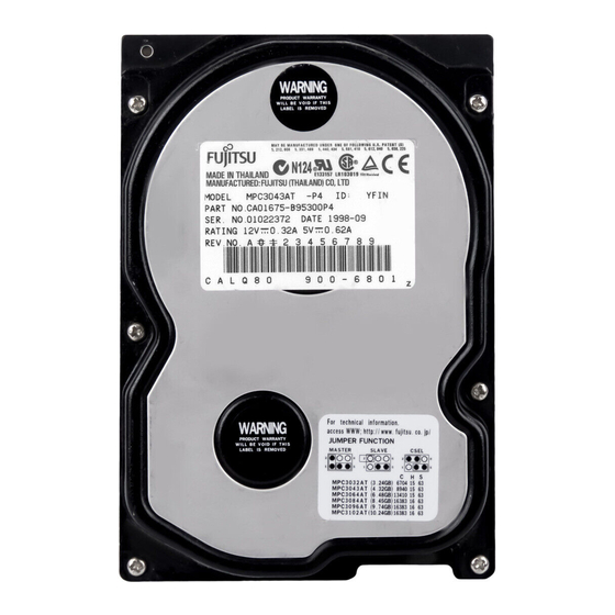
- Page 1 MPC3032AT MPC3043AT MPC3064AT MPC3084AT MPC3096AT MPC3102AT DISK DRIVES PRODUCT MANUAL C141-E055-03EN...
- Page 2 Dec., 1998 Pages 1-4, 1-9, 4-13 to 4-20, 5-30, 5-31, 5-48, 5-49, 5-73, 6-8 to 6-10 revised. Specification No.: C141-E055-**EN The contents of this manual is subject to change without prior notice. All Rights Reserved. Copyright 1998 FUJITSU LIMITED C141-E055-03EN...
- Page 3 This page is intentionally left blank.
- Page 4 PREFACE This manual describes the MPC3032AT, MPC3043AT, MPC3064AT, MPC3084AT, MPC3096AT and MPC3102AT a 3.5-inch hard disk drive with a BUILT-IN controller that is compatible with the ATA interface. This manual explains, in detail, how to incorporate the hard disk drives into user systems. This manual assumes that users have a basic knowledge of hard disk drives and their application in computer systems.
- Page 5 Conventions for Alert Messages This manual uses the following conventions to show the alert messages. An alert message consists of an alert signal and alert statements. The alert signal consists of an alert symbol and a signal word or just a signal word. The following are the alert signals and their meanings: This indicates a hazarous situation likely to result in serious personal injury if the user does not perform the procedure correctly.
- Page 6 "Disk drive defects" refers to defects that involve adjustment, repair, or replacement. Fujitsu is not liable for any other disk drive defects, such as those caused by user misoperation or mishandling, inappropriate operating environments, defects in the power supply or cable, problems of the host system, or other causes outside the disk drive.
- Page 7 This page is intentionally left blank.
-
Page 8: Table Of Contents
CONTENTS page CHAPTER 1 DEVICE OVERVIEW ................... 1 - 1 Features .......................... 1 - 1 1.1.1 Functions and performance .................... 1 - 1 1.1.2 Adaptability........................1 - 2 1.1.3 Interface.......................... 1 - 2 Device Specifications ..................... 1 - 4 1.2.1 Specifications summary.................... - Page 9 3.4.1 Location of setting jumpers .................... 3 - 9 3.4.2 Factory default setting ....................3 - 10 3.4.3 Jumper configuration...................... 3 - 10 CHAPTER 4 THEORY OF DEVICE OPERATION ............4 - 1 Outline..........................4 - 1 Subassemblies ........................ 4 - 1 4.2.1 Disk ..........................
- Page 10 5.2.2 Command block registers ....................5 - 8 5.2.3 Control block registers ....................5 - 13 Host Commands ......................5 - 13 5.3.1 Command code and parameters..................5 - 14 5.3.2 Command descriptions ....................5 - 16 5.3.3 Error posting........................5 - 55 Command Protocol......................
- Page 11 5.6.4.5 Device terminating an Ultra DMA data in burst ............. 5 - 83 5.6.4.6 Host terminating an Ultra DMA data in burst..............5 - 84 5.6.4.7 Initiating an Ultra DMA data out burst................5 - 85 5.6.4.8 Sustained Ultra DMA data out burst................5 - 86 5.6.4.9 Device pausing an Ultra DMA data out burst..............
- Page 12 FIGURES page Current fluctuation (Typ.) when power is turned on............1 - 7 Disk drive outerview ...................... 2 - 1 Configuration of disk media heads................. 2 - 3 1 drive system configuration ..................2 - 4 2 drives configuration..................... 2 - 5 Dimensions........................
- Page 13 Protocol for the command execution without data transfer ..........5 - 60 Normal DMA data transfer ..................... 5 - 62 Ultra DMA termination with pull-up or pull-down ............5 - 73 PIO data transfer timing....................5 - 75 5.10 Single word DMA data transfer timing ................5 - 76 5.11 Multiword DMA data transfer timing (mode 2) .............
- Page 14 TABLES page Specifications ......................... 1 - 4 Model names and product numbers................1 - 5 Current and power dissipation..................1 - 6 Environmental specifications..................1 - 8 Acoustic noise specification ................... 1 - 8 Shock and vibration specification................... 1 - 9 Surface temperature measurement points and standard values ........
- Page 15 This page is intentionally left blank.
-
Page 16: Chapter 1 Device Overview
CHAPTER 1 DEVICE OVERVIEW Features Device Specifications Power Requirements Environmental Specifications Acoustic Noise Shock and Vibration Reliability Error Rate Media Defects Overview and features are described in this chapter, and specifications and power requirement are described. The MPC3032AT, MPC3043AT, MPC3064AT, MPC3084AT, MPC3096AT and MPC3102AT are a 3.5-inch hard disk drive with a built-in ATA controller. -
Page 17: Adaptability
Average positioning time Use of a rotary voice coil motor in the head positioning mechanism greatly increases the positioning speed. The average positioning time is 10 ms (at read). 1.1.2 Adaptability Power save mode The power save mode feature for idle operation, stand by and sleep modes makes the disk drive ideal for applications where power consumption is a factor. - Page 18 Error correction and retry by ECC If a recoverable error occurs, the disk drive itself attempts error recovery. The 24-byte ECC has improved buffer error correction for correctable data errors. Write cache When the disk drive receives a write command, the disk drive posts the command completion at completion of transferring data to the data buffer completion of writing to the disk media.
-
Page 19: Device Specifications
Device Specifications 1.2.1 Specifications summary Table 1.1 shows the specifications of the disk drive. Table 1.1 Specifications MPC3032AT MPC3043AT MPC3064AT MPC3084AT MPC3096AT MPC3102AT Formatted Capacity (*1) 3243.66 MB 4325.52 MB 6488.29 MB 8455.20 MB 9747.58 MB 10242.74 MB Number of Heads Number of Cylinders 11,116 + 120 (User + Alternate &... -
Page 20: Model And Product Number
1.2.2 Model and product number Table 1.2 lists the model names and product numbers. Table 1.2 Model names and product numbers Model Name Capacity Mounting Order No. Others (user area) Screw No. 6-32UNC CA01675-B321 MPC3032AT 3243.66 No. 6-32UNC CA01675-B331 MPC3043AT 4325.52 No. -
Page 21: Current And Power Dissipation
Table 1.3 Current and power dissipation Typical RMS current (*1) [mA] Mode of Typical Power (*2) [watts] Operation +12 V +5 V Model All Models 3032AT 3043AT 3084AT 3032AT 3043AT 3084AT 3064AT 3096AT 3064AT 3096AT 3102AT 3102AT Spin up 1300 17.9 1500 peak 800 peak... -
Page 22: Current Fluctuation (Typ.) When Power Is Turned On
Current fluctuation (Typ.) when power is turned on Note: Maximum current is 1.5 A and is continuance is 1.5 seconds Figure 1.1 Current fluctuation (Typ.) when power is turned on Power on/off sequence The voltage detector circuit monitors +5 V and +12 V. The circuit does not allow a write signal if either voltage is abnormal. -
Page 23: Environmental Specifications
Environmental Specifications Table 1.4 lists the environmental specifications. Table 1.4 Environmental specifications Temperature • Operating 5°C to 55°C (ambient) 5°C to 60°C (disk enclosure surface) • Non-operating –40°C to 60°C • Thermal Gradient 20°C/h or less Humidity • Operating 8% to 80%RH (Non-condensing) •... -
Page 24: Shock And Vibration
Shock and Vibration Table 1.6 lists the shock and vibration specification. Table 1.6 Shock and vibration specification Vibration (swept sine, one octave per minute) • Operating 5 to 300 Hz, 0.5G-0-peak (without non-recovered errors) • Non-operating 5 to 400 Hz, 4G-0-peak (no damage) Shock (half-sine pulse, 11 ms duration) •... -
Page 25: Error Rate
Data assurance in the event of power failure Except for the data block being written to, the data on the disk media is assured in the event of any power supply abnormalities. This does not include power supply abnormalities during disk media initialization (formatting) or processing of defects (alternative block assignment). -
Page 26: Chapter 2 Device Configuration
CHAPTER 2 DEVICE CONFIGURATION Device Configuration System Configuration Device Configuration Figure 2.1 shows the disk drive. The disk drive consists of a disk enclosure (DE), read/write preamplifier, and controller PCA. The disk enclosure contains the disk media, heads, spindle motors actuators, and a circulating air filter. Figure 2.1 Disk drive outerview C141-E055-01EN... - Page 27 Disk The outer diameter of the disk is 95 mm. The inner diameter is 25 mm. The number of disks used varies with the model, as described below. The disks are rated at over 40,000 start/stop operations. MPC3032AT: 1 disk MPC3043AT: 2 disks MPC3064AT: 2 disks MPC3084AT: 3 disks...
-
Page 28: Configuration Of Disk Media Heads
MPC3032AT Model Spindle Actuator MPC3043AT Model MPC3064AT Model Spindle Actuator Spindle Actuator MPC3084AT/MPC3096AT/MPC3102AT Model Spindle Actuator Figure 2.2 Configuration of disk media heads Spindle motor The disks are rotated by a direct drive Hall-less DC motor. Actuator The actuator uses a revolving voice coil motor (VCM) structure which consumes low power and generates very little heat. -
Page 29: System Configuration
Air circulation system The disk enclosure (DE) is sealed to prevent dust and dirt from entering. The disk enclosure features a closed loop air circulation system that relies on the blower effect of the rotating disk. This system continuously circulates the air through the recirculation filter to maintain the cleanliness of the air in the disk enclosure. -
Page 30: Drives Connection
2.2.3 2 drives connection Host Disk drive #0 (Host adaptor) AT bus (Host interface) Disk drive #1 ATA interface Note: When the drive that is not conformed to ATA is connected to the disk drive is above configuration, the operation is not guaranteed. Figure 2.4 2 drives configuration IMPORTANT... - Page 31 This page is intentionally left blank.
-
Page 32: Chapter 3 Installation Conditions
CHAPTER 3 INSTALLATION CONDITIONS Dimensions Mounting Cable Connections Jumper Settings Dimensions Figure 3.1 illustrates the dimensions of the disk drive and positions of the mounting screw holes. All dimensions are in mm. C141-E055-01EN 3 - 1... -
Page 33: Dimensions
Figure 3.1 Dimensions 3 - 2 C141-E055-02EN... -
Page 34: Mounting
Mounting Orientation Figure 3.2 illustrates the allowable orientations for the disk drive. The mounting angle can vary ±5° from the horizontal. gravity (a) Horizontal mounting (b) Vertical mounting –1 (c) Vertical mounting –2 Figure 3.2 Orientation Frame The disk enclosure (DE) body is connected to signal ground (SG) and the mounting frame is also connected to signal ground. -
Page 35: Limitation Of Side-Mounting
Use these screw holes Do not use this screw holes Figure 3.3 Limitation of side-mounting Side surface mounting Bottom surface mounting Frame of system Frame of system cabinet cabinet 4.5 or less Screw Screw 5.0 or less Details of A Details of B Figure 3.4 Mounting frame structure... -
Page 36: Surface Temperature Measurement Points
Ambient temperature The temperature conditions for a disk drive mounted in a cabinet refer to the ambient temperature at a point 3 cm from the disk drive. Pay attention to the air flow to prevent the DE surface temperature from exceeding 60°C. Provide air circulation in the cabinet such that the PCA side, in particular, receives sufficient cooling. -
Page 37: Service Area
Service area Figure 3.6 shows how the drive must be accessed (service areas) during and after installation. - Mounting screw hole [Q side] - Mounting screw hole [R side] [P side] - Mounting screw hole - Cable connection - Mode setting switches Figure 3.6 Service area External magnetic fields... -
Page 38: Cable Connections
Cable Connections 3.3.1 Device connector The disk drive has the connectors and terminals listed below for connecting external devices. Figure 3.7 shows the locations of these connectors and terminals. Power supply connector (CN1) ATA interface connector (CN1) Power supply connector (CN1) Mode Setting Pins... -
Page 39: Cable Connector Specifications
Cable connector specifications Table 3.2 lists the recommended specifications for the cable connectors. Table 3.2 Cable connector specifications Name Model Manufacturer Cable socket FCN-707B040-AU/B Fujitsu (closed-end type) ATA interface cable Cable socket (40-pin, CN1) FCN-707B040-AU/O Fujitsu (through-end type) Signal cable... -
Page 40: Power Supply Connector (Cn1)
3.3.4 Power supply connector (CN1) Figure 3.9 shows the pin assignment of the power supply connector (CN1). +12VDC +12V RETURN +5V RETURN +5VDC (Viewed from cable side) Figure 3.9 Power supply connector pins (CN1) Jumper Settings 3.4.1 Location of setting jumpers Figure 3.10 shows the location of the jumpers to select drive configuration and functions. -
Page 41: Factory Default Setting
3.4.2 Factory default setting Figure 3.11 shows the default setting position at the factory. (Master device setting) Figure 3.11 Factory default setting 3.4.3 Jumper configuration Device type Master device (device #0) or slave device (device #1) is selected. (a) Master device (b) Slave device Figure 3.12 Jumper setting of master or slave device Cable Select (CSEL) -
Page 42: Jumper Setting Of Cable Select
CSEL connected to the interface Cable selection can be done by the special interface cable. Figure 3.13 Jumper setting of Cable Select Figures 3.14 and 3.15 show examples of cable selection using unique interface cables. By connecting the CSEL of the master device to the CSEL Line (conductor) of the cable and connecting it to ground further, the CSEL is set to low level. - Page 43 Special setting 1 (SP1) The number of cylinders reported by the IDENTIFY DEVICE command is selected. (a) Default mode Master Device Slave Device Cable Select Model No. of cylinders No. of heads No. of sectors MPC3032AT 6,704 MPC3043AT 8,940 MPC3064AT 13,410 MPC3084AT 16,383...
-
Page 44: Chapter 4 Theory Of Device Operation
CHAPTER 4 THEORY OF DEVICE OPERATION Outline Subassemblies Circuit Configuration Power-on sequence Self-calibration Read/Write Circuit Servo Control This chapter explains basic design concepts of the disk drive. Also, this chapter explains subassemblies of the disk drive, each sequence, servo control, and electrical circuit blocks. Outline This chapter consists of two parts. -
Page 45: Head
4.2.2 Head Figure 4.1 shows the read/write head structures. The MPC3032AT has 2 read/write heads, the MPC3043AT has 3, MPC3064AT has 4, MPC3084AT, MPC3096AT and MPC3102AT has 6. These heads are raised from the disk surface as the spindle motor approaches the rated rotation speed. -
Page 46: Spindle
4.2.3 Spindle The spindle consists of a disk stack assembly and spindle motor. The disk stack assembly is activated by the direct drive sensor-less DC spindle motor, which has a speed of 5,400 rpm ±0.5%. The spindle is controlled with detecting a PHASE signal generated by counter electromotive voltage of the spindle motor at starting. -
Page 47: Circuit Configuration
Circuit Configuration Figure 4.2 shows the disk drive circuit configuration. Read/write circuit The read/write circuit consists of two LSIs; read/write preamplifier (PreAMP) and read channel (RDC). The PreAMP consists of the write current switch circuit, that flows the write current to the head coil, and the voltage amplifier circuit, that amplitudes the read output from the head. -
Page 48: Mpc30Xxat Block Diagram
Figure 4.2 MPC30xxAT Block diagram C141-E055-01EN 4 - 5... -
Page 49: Power-On Sequence
Power-on Sequence Figure 4.3 describes the operation sequence of the disk drive at power-on. The outline is described below. a) After the power is turned on, the disk drive executes the MPU bus test, internal register read/write test, and work RAM read/write test. When the self-diagnosis terminates successfully, the disk drive starts the spindle motor. -
Page 50: Power-On Operation Sequence
Power on Start Self-diagnosis 1 • MPU bus test • Inner register write/read test • Work RAM write/read test The spindle motor starts. Self-diagnosis 2 • Data buffer write/read test Confirming spindle motor speed Release heads from actuator lock Initial on-track and read out of system information Execute self-calibration Drive ready state... -
Page 51: Self-Calibration
Self-calibration The disk drive occasionally performs self-calibration in order to sense and calibrate mechanical external forces on the actuator, and VCM torque. This enables precise seek and read/write operations. 4.5.1 Self-calibration contents Sensing and compensating for external forces The actuator suffers from torque due to the FPC forces and winds accompanying disk revolution. -
Page 52: Execution Timing Of Self-Calibration
4.5.2 Execution timing of self-calibration Self-calibration is executed when: The power is turned on. The disk drive receives the RECALIBRATE command from the host. The self-calibration execution timechart of the disk drive specifies self-calibration. The disk drive performs self-calibration according to the timechart based on the time elapsed from power-on. -
Page 53: Read/Write Circuit
Read/write Circuit The read/write circuit consists of the read/write preamplifier (PreAMP), the write circuit, the read circuit, and the time base generator in the read channel (RDC). Figure 4.4 is a block diagram of the read/write circuit. 4.6.1 Read/write preamplifier (PreAMP) One PreAMP is mounted on the FPC. -
Page 54: Read/Write Circuit Block Diagram
Figure 4.4 Read/write circuit block diagram C141-E055-01EN 4 - 11... -
Page 55: Read Circuit
4.6.3 Read circuit The head read signal from the PreAMP is regulated by the automatic gain control (AGC) circuit. Then the output is converted into the sampled read data pulse by the programmable filter circuit and the adaptive equalizer circuit. This clock signal is converted into the NRZ data by the 16/17 GCR decoder circuit based on the read data maximum-likelihood-detected by the Viterbi detection circuit, then is sent to the HDC. -
Page 56: Time Base Generator Circuit
4.6.4 Time base generator circuit The drive uses constant density recording to increase total capacity. This is different from the conventional method of recording data with a fixed data transfer rate at all data area. In the constant density recording method, data area is divided into zones by radius and the data transfer rate is set so that the recording density of the inner cylinder of each zone is nearly constant. -
Page 57: Servo Control
Servo Control The actuator motor and the spindle motor are submitted to servo control. The actuator motor is controlled for moving and positioning the head to the track containing the desired data. To turn the disk at a constant velocity, the actuator motor is controlled according to the servo data that is written on the data side beforehand. -
Page 58: Physical Sector Servo Configuration On Disk Surface
b. Move head to reference cylinder Drives the VCM to position the head at the any cylinder in the data area. The logical initial cylinder is at the outermost circumference (cylinder 0). c. Seek to specified cylinder Drives the VCM to position the head to the specified cylinder. d. -
Page 59: Data-Surface Servo Format
Servo burst capture circuit The four servo signals can be synchronously detected by the STROB signal, full-wave rectified integrated. A/D converter (ADC) The A/D converter (ADC) receives the servo signals are integrated, converts them to digital, and transfers the digital signal to the DSP unit. D/A converter (DAC) The D/A converter (DAC) converts the VCM drive current value (digital value) calculated by the DSP unit into analog values and transfers them to the power amplifier. -
Page 60: Servo Frame Format
Data area This area is used as the user data area SA area. Outer guard band This area is located at outer position of the user data area, and the rotational speed of the spindle can be controlled on this cylinder area for head moving. 4.7.3 Servo frame format As the servo information, the drive uses the two-phase servo generated from the gray code and... -
Page 61: Actuator Motor Control
Gray code (including index bit) This area is used as cylinder address. The data in this area is converted into the binary data by the gray code demodulation circuit. Servo A, servo B, servo C, servo D This area is used as position signals between tracks, and the IDD control at on-track so that servo A level equals to servo B level. -
Page 62: Spindle Motor Control
(called SVC hereafter). The firmware operates on the MPU manufactured by Fujitsu. The spindle motor is controlled by sending several signals from the MPU to the SVC. There are three modes for the spindle control;... - Page 63 Acceleration mode In this mode, the MPU stops to send the phase switching signal to the SVC. The SVC starts a phase switching by itself based on the counter electromotive force. Then, rotation of the spindle motor accelerates. The MPU calculates a rotational speed of the spindle motor based on the PHASE signal from the SVC, and accelerates till the rotational speed reaches 5,400 rpm.
-
Page 64: Chapter 5 Interface
CHAPTER 5 INTERFACE Physical Interface Logical Interface Host Commands Command Protocol Ultra DMA feature Set Timing C141-E055-01EN 5 - 1... -
Page 65: Physical Interface
Physical Interface 5.1.1 Interface signals Figure 5.1 shows the interface signals. Host DD(15:0) DATA BUS DMACK-: DMA ACKNOWLEDGE DMARQ: DMA REQUEST DIOW-: I/O WRITE DIOR- : I/O READ INTRQ : INTERRUPT REQUEST IOCS16-: IOCS 16 PDIAG- : PASSED DIAGNOSTIC IORDY : I/O CHANNEL READY DASP- : DEVICE ACTIVE/DEVICE 1 PRESENT DA 0-2: DEVICE ADDRESS CS0- : CHIP SELECT 0... -
Page 66: Signal Assignment On The Connector
5.1.2 Signal assignment on the connector Table 5.1 shows the signal assignment on the interface connector. Table 5.1 Signal assignment on the interface connector Pin No. Signal Pin No. Signal RESET– DATA7 DATA8 DATA6 DATA9 DATA5 DATA10 DATA4 DATA11 DATA3 DATA12 DATA2 DATA13... - Page 67 [signal] [I/O] [Description] DIOR–, DIOR– is the strobe signal asserted by the host to read device HDMARDY–, registers or the data port. HSTROBE HDMARDY– is a flow control signal for Ultra DMA data in bursts. This signal is asserted by the host to indicate to the device that the host is ready to receive Ultra DMA data in bursts.
- Page 68 [signal] [I/O] [Description] IORDY, This signal is negated to extend the host transfer cycle of any host DDMARDY–, register access (Read or Write) when the device is not ready to DSTROBE respond to a data transfer request. DDMARDY– is a flow control signal for Ultra DMA data out bursts.
-
Page 69: Logical Interface
Logical Interface The device can operate for command execution in either address-specified mode; cylinder- head-sector (CHS) or Logical block address (LBA) mode. The IDENTIFY DEVICE information indicates whether the device supports the LBA mode. When the host system specifies the LBA mode by setting bit 6 in the Device/Head register to 1, HS3 to HS0 bits of the Device/Head register indicates the head No. -
Page 70: Command Block Registers
Table 5.2 I/O registers I/O registers Host I/O CS0– CS1– address Read operation Write operation Command block registers Data Data X'1F0' Error Register Features X'1F1' Sector Count Sector Count X'1F2' Sector Number Sector Number X'1F3' Cylinder Low Cylinder Low X'1F4' Cylinder High Cylinder High X'1F5'... - Page 71 5.2.2 Command block registers Data register (X'1F0') The Data register is a 16-bit register for data block transfer between the device and the host system. Data transfer mode is PIO or LBA mode. Error register (X'1F1') The Error register indicates the status of the command executed by the device. The contents of this register are valid when the ERR bit of the Status register is 1.
-
Page 72: Diagnostic Code
[Diagnostic code] X'01': No Error Detected. X'03': Data Buffer Compare Error. X'05': ROM Sum Check Error. X'80': Device 1 (slave device) Failed. Error register of the master device is valid under two devices (master and slave) configuration. If the slave device fails, the master device posts X’80’ OR (the diagnostic code) with its own status (X'01' to X'05'). - Page 73 Cylinder Low register (X'1F4') The contents of this register indicates low-order 8 bits of the starting cylinder address for any disk-access. At the end of a command, the contents of this register are updated to the current cylinder number. Under the LBA mode, this register indicates LBA bits 15 to 8. Cylinder High register (X'1F5') The contents of this register indicates high-order 8 bits of the disk-access start cylinder address.
- Page 74 Status register (X'1F7') The contents of this register indicate the status of the device. The contents of this register are updated at the completion of each command. When the BSY bit is cleared, other bits in this register should be validated within 400 ns. When the BSY bit is 1, other bits of this register are invalid.
- Page 75 - Bit 3: Data Request (DRQ) bit. This bit indicates that the device is ready to transfer data of word unit or byte unit between the host system and the device. - Bit 2: Always 0. - Bit 1: Always 0. - Bit 0: Error (ERR) bit.
-
Page 76: Host Commands
5.2.3 Control block registers Alternate Status register (X'3F6') The Alternate Status register contains the same information as the Status register of the command block register. The only difference from the Status register is that a read of this register does not imply Interrupt Acknowledge and INTRQ signal is not reset. -
Page 77: Command Code And Parameters
5.3.1 Command code and parameters Table 5.3 lists the supported commands, command code and the registers that needed parameters are written. Table 5.3 Command code and parameters (1 of 2) Command code (Bit) Parameters used Command name FR SC SN CY DH READ SECTOR(S) READ MULTIPLE READ DMA... - Page 78 Table 5.3 Command code and parameters (2 of 2) Command code (Bit) Parameters used Command name FR SC SN CY DH STANDBY IMMEDIATE SLEEP CHECK POWER MODE SMART FLUSH CACHE Notes: FR : Features Register CY: Cylinder Registers SC : Sector Count Register DH : Drive/Head Register SN : Sector Number Register R: Retry at error...
-
Page 79: Command Descriptions
5.3.2 Command descriptions The contents of the I/O registers to be necessary for issuing a command and the example indication of the I/O registers at command completion are shown as following in this subsection. Example: READ SECTOR(S) WITH RETRY At command issuance (I/O registers setting contents) (CM) (DH) Head No. - Page 80 Note: When the L bit is specified to 1, the lower 4 bits of the DH register and all bits of the CH, CL and SN registers indicate the LBA bits (bits of the DH register are the MSB (most significant bit) and bits of the SN register are the LSB (least significant bit). At error occurrence, the SC register indicates the remaining sector count of data transfer.
- Page 81 At command completion (I/O registers contents to be read) (ST) Status information (DH) End head No. /LBA [MSB] (CH) End cylinder No. [MSB] / LBA (CL) End cylinder No. [LSB] / LBA (SN) End sector No. / LBA [LSB] (SC) 00 (*1) (ER) Error information...
-
Page 82: Execution Example Of Read Multiple Command
Figure 5.2 shows an example of the execution of the READ MULTIPLE command. Block count specified by SET MULTIPLE MODE command = 4 (number of sectors in a block) READ MULTIPLE command specifies; Number of requested sectors = 9 (Sector Count register = 9) Number of sectors in incomplete block = remainder of 9/4 =1 Command Issue Parameter... - Page 83 Note: If the command is terminated due to an error, the remaining number of sectors for which data was not transferred is set in this register. READ DMA (X'C8' or X'C9') This command operates similarly to the READ SECTOR(S) command except for following events.
- Page 84 At command completion (I/O registers contents to be read) (ST) Status information (DH) End head No. /LBA [MSB] (CH) End cylinder No. [MSB] / LBA (CL) End cylinder No. [LSB] / LBA (SN) End sector No. / LBA [LSB] (SC) 00 (*1) (ER) Error information...
- Page 85 At command completion (I/O registers contents to be read) (ST) Status information (DH) End head No. /LBA [MSB] (CH) End cylinder No. [MSB] / LBA (CL) End cylinder No. [LSB] / LBA (SN) End sector No. / LBA [LSB] (SC) 00 (*1) (ER) Error information...
- Page 86 At command completion (I/O registers contents to be read) (ST) Status information (DH) End head No. /LBA [MSB] (CH) End cylinder No. [MSB] / LBA (CL) End cylinder No. [LSB] / LBA (SN) End sector No. / LBA [LSB] (SC) 00 (*1) (ER) Error information...
- Page 87 The contents of the command block registers related to addresses after the transfer of a data block containing an erred sector are undefined. To obtain a valid error information, the host should retry data transfer as an individual requests. At command issuance (I/O registers setting contents) (CM) (DH) Start head No.
- Page 88 1) Single word DMA transfer mode 2: Sets the FR register = X'03' and SC register = X'12' by the SET FEATURES command 2) Multiword DMA transfer mode 2: Sets the FR register = X'03' and SC register = X'22' by the SET FEATURES command 3) Ultra DMA transfer mode 2: Sets the FR register = X'03' and SC register = X'42' by the SET FEATURES...
- Page 89 At command issuance (I/O registers setting contents) (CM) (DH) Start head No. /LBA [MSB] (CH) Start cylinder No. [MSB]/ LBA (CL) Start cylinder No. [LSB] / LBA (SN) Start sector No. / LBA [LSB] (SC) Transfer sector count (FR) R = 0 with Retry R = 1 without Retry...
- Page 90 At command completion (I/O registers contents to be read) (ST) Status information (DH) (CH) (CL) (SN) (SC) (ER) Error information (10) SEEK (X'7x', x : X'0' to X'F') This command performs a seek operation to the track and selects the head specified in the command block registers.
- Page 91 (11) INITIALIZE DEVICE PARAMETERS (X'91') The host system can set the number of sectors per track and the maximum head number (maximum head number is "number of heads minus 1") per cylinder with this command. Upon receipt of this command, the device sets the BSY bit of Status register and saves the parameters.
- Page 92 At command issuance (I/O registers setting contents) (CM) (DH) (CH) (CL) (SN) (SC) (FR) At command completion (I/O registers contents to be read) (ST) Status information (DH) (CH) (CL) (SN) (SC) (ER) Error information C141-E055-01EN 5 - 29...
-
Page 93: Information To Be Read By Identify Device Command
Table 5.4 Information to be read by IDENTIFY DEVICE command (1 of 3) Word Value Description X‘045A’ General Configuration *1 X‘1A30’ Number of cylinders MPC3032AT: X‘1A30’ X‘22EC’ MPC3043AT: X‘22EC’ X‘3462’ MPC3064AT: X‘3462’ X‘3FFF’ MPC3084AT: X‘3FFF’ X‘3FFF’ MPC3096AT: X‘3FFF’ X‘3FFF’ MPC3102AT: X‘3FFF’ X‘0000’... - Page 94 Table 5.4 Information to be read by IDENTIFY DEVICE command (2 of 3) Word Value Description 89-127 X‘00’ Reserved X‘00’ Security status not supported 129-159 X‘00’ Reserved 160-255 X‘00’ Reserved *1 Word 0: General configuration Bit 15: 0 = ATA device Bit 14-8: Vendor specific Bit 7: 1 = Removable media device Bit 6: 1 = not removable controller and/or device...
- Page 95 Table 5.4 Information to be read by IDENTIFY DEVICE command (3 of 3) *8 Word 59: Transfer sector count currently set by READ/WRITE MULTIPLE command Bit 15-9: Reserved Bit 8: Multiple sector transfer 1=Enable Bit 7-0: Transfer sector count currently set by READ/WRITE MULTIPLE without interrupt supports 2, 4, 8, 16 and 32 sectors.
- Page 96 (13) IDENTIFY DEVICE DMA (X'EE') When this command is not used to transfer data to the host in DMA mode, this command functions in the same way as the Identify Device command. At command issuance (I/O registers setting contents) (CM) (DH) (CH) (CL)
-
Page 97: Features Register Values And Settable Modes
Table 5.5 Features register values and settable modes Features Register Drive operation mode X‘02’ Enables the write cache function. X‘03’ Specifies the transfer mode. Supports PIO mode 4, single word DMA mode 2, and multiword DMA mode regardless of Sector Count register contents. X‘55’... - Page 98 The host sets X'03' to the Features register. By issuing this command with setting a value to the Sector Count register, the transfer mode can be selected. Upper 5 bits of the Sector Count register defines the transfer type and lower 3 bits specifies the binary mode value. However, the IDD can operate with the PIO transfer mode 4 and multiword DMA transfer mode 2 regardless of reception of the SET FEATURES command for transfer mode setting.
- Page 99 At command issuance (I/O registers setting contents) (CM) (DH) (CH) (CL) (SN) (SC) Sector count/block (FR) At command completion (I/O registers contents to be read) (ST) Status information (DH) (CH) (CL) (SN) (SC) Sector count/block (ER) Error information After power-on or after hardware reset, the READ MULTIPLE and WRITE MULTIPLE command operation are disabled as the default mode.
- Page 100 (16) EXECUTE DEVICE DIAGNOSTIC (X'90') This command performs an internal diagnostic test (self-diagnosis) of the device. This command usually sets the DRV bit of the Drive/Head register is to 0 (however, the DV bit is not checked). If two devices are present, both devices execute self-diagnosis. If device 1 is present: Both devices shall execute self-diagnosis.
- Page 101 At command issuance (I/O registers setting contents) (CM) (DH) (CH) (CL) (SN) (SC) (FR) At command completion (I/O registers contents to be read) (ST) Status information (DH) (CH) (CL) (SN) (*1) (SC) (ER) Diagnostic code *1 This register indicates X‘00’ in the LBA mode. (17) FORMAT TRACK (X'50') Upon receipt of this command, the device sets the DRQ bit and waits the completion of 512-...
- Page 102 At command issuance (I/O registers setting contents) (CM) (DH) Head No. /LBA [MSB] (CH) Cylinder No. [MSB] / LBA (CL) Cylinder No. [LSB] / LBA (SN) Sector No. / LBA [LSB] (SC) Number of sectors to be transferred (FR) R = 0 with Retry R = 1 without Retry...
- Page 103 At command issuance (I/O registers setting contents) (CM) (DH) Head No. /LBA [MSB] (CH) Cylinder No. [MSB] / LBA (CL) Cylinder No. [LSB] / LBA (SN) Sector No. / LBA [LSB] (SC) Number of sectors to be transferred (FR) R = 0 with Retry R = 1 without Retry...
- Page 104 At command completion (I/O registers contents to be read) (ST) Status information (DH) (CH) (CL) (SN) (SC) (ER) Error information (21) WRITE BUFFER (X'E8') The host system can overwrite the contents of the sector buffer of the device with a desired data pattern by issuing this command.
- Page 105 (22) IDLE (X'97' or X'E3') Upon receipt of this command, the device sets the BSY bit of the Status register, and enters the idle mode. Then, the device clears the BSY bit, and generates an interrupt. The device generates an interrupt even if the device has not fully entered the idle mode. If the spindle of the device is already rotating, the spin-up sequence shall not be implemented.
- Page 106 At command completion (I/O registers contents to be read) (ST) Status information (DH) (CH) (CL) (SN) (SC) (ER) Error information (23) IDLE IMMEDIATE (X'95' or X'E1') Upon receipt of this command, the device sets the BSY bit of the Status register, and enters the idle mode.
- Page 107 (24) STANDBY (X'96' or X'E2') Upon receipt of this command, the device sets the BSY bit of the Status register and enters the standby mode. The device then clears the BSY bit and generates an interrupt. The device generates an interrupt even if the device has not fully entered the standby mode. If the device has already spun down, the spin-down sequence is not implemented.
- Page 108 At command issuance (I/O registers setting contents) (CM) X'94' or X'E0' (DH) (CH) (CL) (SN) (SC) (FR) At command completion (I/O registers contents to be read) (ST) Status information (DH) (CH) (CL) (SN) (SC) (ER) Error information (26) SLEEP (X'99' or X'E6') This command is the only way to make the device enter the sleep mode.
- Page 109 At command completion (I/O registers contents to be read) (ST) Status information (DH) (CH) (CL) (SN) (SC) (ER) Error information (27) CHECK POWER MODE (X'98' or X'E5') The host checks the power mode of the device with this command. The host system can confirm the power save mode of the device by analyzing the contents of the Sector Count and Sector registers.
- Page 110 At command issuance (I/O registers setting contents) (CM) X'98' or X'E5' (DH) (CH) (CL) (SN) (SC) (FR) At command completion (I/O registers contents to be read) (ST) Status information (DH) (CH) (CL) (SN) (SC) X'00' or X'FF' (ER) Error information (28) SMART (X'B0) This command performs operations for device failure predictions according to a subcommand...
-
Page 111: Features Register Values (Subcommands) And Functions
Table 5.7 Features Register values (subcommands) and functions Features Resister Function X’D0’ SMART Read Attribute Values: A device that received this subcommand asserts the BSY bit and saves all the updated attribute values. The device then clears the BSY bit and transfers 512- byte attribute value information to the host. - Page 112 Alternative, the device must issue the SMART Enable-Disable Attribute AutoSave subcommand (FR register = D2h) to use a feature which regularly save the device attribute value data to a medium. The host can predict failures in the device by periodically issuing the SMART Return Status subcommand (FR register = DAh) to reference the CL and CH registers.
-
Page 113: Format Of Device Attribute Value Data
The attribute value information is 512-byte data; the format of this data is shown below. The host can access this data using the SMART Read Attribute Values subcommand (FR register = D0h). The insurance failure threshold value data is 512-byte data; the format of this data is shown below. -
Page 114: Format Of Insurance Failure Threshold Value Data
Table 5.9 Format of insurance failure threshold value data Byte Item Data format version number Attribute 1 Attribute ID Insurance failure threshold Threshold 1 (Threshold of Reserved attribute 1) Threshold 2 to (The format of each threshold value is the same as threshold 30 that of bytes 02 to 0D.) Reserved... - Page 115 Attribute ID The attribute ID is defined as follows: Attribute ID Attribute name (Indicates unused attribute data.) Read error rate Throughput performance Spin up time Number of times the spindle motor is activated Number of alternative sectors Seek error rate Seek time performance Power-on time Number of retries made to activate the spindle motor...
- Page 116 Raw attribute value Raw attributes data is retained. Failure prediction capability flag Bit 0: The attribute value data is saved to a medium before the device enters power saving mode. Bit 1: The device automatically saves the attribute value data to a medium after the previously set operation.
- Page 117 (29) FLUSH CACHE (X ‘E7’) This command is use by the host to request the device to flush the write cache. If the write cache is to be flushed, all data cached shall be written to the media. The BSY bit shall remain set to one until all data has been successfully written or an error occurs.
-
Page 118: Error Posting
5.3.3 Error posting Table 5.10 lists the defined errors that are valid for each command. Table 5.10 Command code and parameters Command name Error register (X'1F1') Status register (X'1F7') ICRC INDF ABRT TR0NF DRDY READ SECTOR(S) WRITE SECTOR(S) READ MULTIPLE WRITE MULTIPLE READ DMA WRITE DMA... -
Page 119: Command Protocol
Command Protocol The host should confirm that the BSY bit of the Status register of the device is 0 prior to issue a command. If BSY bit is 1, the host should wait for issuing a command until BSY bit is cleared to 0. -
Page 120: Read Sector(S) Command Protocol
Command Parameter write Status read Status read • • • • DRDY • • • • INTRQ Data transfer Expanded Command Min. 30 s (*1) • • • INTRQ Data Reg. Selection • • • • Data • • • • •... -
Page 121: Data Transferring Commands From Host To Device
Note: For transfer of a sector of data, the host needs to read Status register (X'1F7') in order to clear INTRQ (interrupt) signal. The Status register should be read within a period from the DRQ setting by the device to 50 s after the completion of the sector data transfer. Note that the host does not need to read the Status register for the reading of a single sector or the last sector in multiple-sector reading. -
Page 122: Write Sector(S) Command Protocol
c) When the device is ready to receive the data of the first sector, the device sets DRQ bit and clears BSY bit. d) The host writes one sector of data through the Data register. e) The device clears the DRQ bit and sets the BSY bit. f) When the drive completes transferring the data of the sector, the device clears BSY bit and asserts INTRQ signal. -
Page 123: Commands Without Data Transfer
Note: For transfer of a sector of data, the host needs to read Status register (X'1F7') in order to clear INTRQ (interrupt) signal. The Status register should be read within a period from the DRQ setting by the device to 50 s after the completion of the sector data transfer. Note that the host does not need to read the Status register for the first and the last sector to be transferred. -
Page 124: Other Commands
5.4.4 Other commands READ MULTIPLE SLEEP WRITE MULTIPLE See the description of each command. 5.4.5 DMA data transfer commands READ DMA WRITE DMA Starting the DMA transfer command is the same as the READ SECTOR(S) or WRITE SECTOR(S) command except the point that the host initializes the DMA channel preceding the command issuance. -
Page 125: Normal Dma Data Transfer
Command Status read Parameter write • • DRDY INTRQ • • • • Data transfer Expanded [Single Word DMA transfer] • • • • DMARQ • • • • DMACK- • • • • IOR- or • • • • IOW- Word [Multiword DMA transfer]... -
Page 126: Ultra Dma Feature Set
Ultra DMA feature set 5.5.1 Overview Ultra DMA is a data transfer protocol used with the READ DMA and WRITE DMA commands. When this protocol is enabled it shall be used instead of the Multiword DMA protocol when these commands are issued by the host. This protocol applies to the Ultra DMA data burst only. -
Page 127: Phases Of Operation
5.5.2 Phases of operation An Ultra DMA data transfer is accomplished through a series of Ultra DMA data in or data out bursts. Each Ultra DMA burst has three mandatory phases of operation: the initiation phase, the data transfer phase, and the Ultra DMA burst termination phase. In addition, an Ultra DMA burst may be paused during the data transfer phase (see 5.5.3 and 5.5.4 for the detailed protocol descriptions for each of these phases, 5.6.4 defines the specific timing requirements). -
Page 128: The Data In Transfer
11) The device shall drive the first word of the data transfer onto DD (15:0). This step may occur when the device first drives DD (15:0) in step (10). 12) To transfer the first word of data the device shall negate DSTROBE within t after the host has negated STOP and asserted HDMARDY-. -
Page 129: Terminating An Ultra Dma Data In Burst
The device shall stop generating DSTROBE edges within t of the host negating HDMARDY-. If the host negates HDMARDY- within t after the device has generated a DSTROBE edge, then the host shall be prepared to receive zero or one additional data words. - Page 130 10) The device shall latch the host's CRC data from DD (15:0) on the negating edge of DMACK-. 11) The device shall compare the CRC data received from the host with the results of its own CRC calculation. If a miscompare error occurs during one or more Ultra DMA bursts for any one command, at the end of the command the device shall report the first error that occurred (see 5.5.5).
-
Page 131: Ultra Dma Data Out Commands
10) If the host has not placed the result of its CRC calculation on DD (15:0) since first driving DD (15:0) during (9), the host shall place the result of its CRC calculation on DD (15:0) (see 5.5.5). 11) The host shall negate DMACK- no sooner than t after the device has asserted DSTROBE and negated DMARQ and the host has asserted STOP and negated HDMARDY-, and no sooner than t... -
Page 132: The Data Out Transfer
9) The device shall assert DDMARDY- within t after the host has negated STOP. After asserting DMARQ and DDMARDY- the device shall not negate either signal until after the first negation of HSTROBE by the host. 10) The host shall drive the first word of the data transfer onto DD (15:0). This step may occur any time during Ultra DMA burst initiation. -
Page 133: Terminating An Ultra Dma Data Out Burst
b) Device pausing an Ultra DMA data out burst The device shall not pause an Ultra DMA burst until at least one data word of an Ultra DMA burst has been transferred. The device shall pause an Ultra DMA burst by negating DDMARDY-. The host shall stop generating HSTROBE edges within t of the device negating DDMARDY-. - Page 134 The device shall compare the CRC data received from the host with the results of its own CRC calculation. If a miscompare error occurs during one or more Ultra DMA bursts for any one command, at the end of the command, the device shall report the first error that occurred (see 5.5.5).
-
Page 135: Ultra Dma Crc Rules
11) The device shall compare the CRC data received from the host with the results of its own CRC calculation. If a miscompare error occurs during one or more Ultra DMA bursts for any one command, at the end of the command, the device shall report the first error that occurred (see 5.5.5). -
Page 136: Series Termination Required For Ultra Dma
I) The CRC generator polynomial is : G (X) = X16 + X12 + X5 + 1. Note: Since no bit clock is available, the recommended approach for calculating CRC is to use a word clock derived from the bus strobe. The combinational logic shall then be equivalent to shifting sixteen bits serially through the generator polynominal where DD0 is shifted in first and DD15 is shifted in last. -
Page 137: Timing
Timing 5.6.1 PIO data transfer Figure 5.9 shows of the data transfer timing between the device and the host system. 5 - 74 C141-E055-01EN... -
Page 138: Pio Data Transfer Timing
Addresses DIOR-/DIOW- Write data DD0-DD15 Read data DD0-DD15 IOCS16- IORDY Symbol Timing parameter Min. Max. Unit Cycle time — Data register selection setup time for DIOR-/DIOW- — Pulse width of DIOR-/DIOW- — Recovery time of DIOR-/DIOW- — Data setup time for DIOW- —... -
Page 139: Single Word Dma Data Transfer
5.6.2 Single word DMA data transfer Figure 5.10 show the single word DMA data transfer timing between the device and the host system. DMARQ DMACK- DIOR-/DIOW- Write data DD0-DD15 Read data DD0-DD15 Symbol Timing parameter Min. Max. Unit Cycle time —... -
Page 140: Multiword Data Transfer
5.6.3 Multiword data transfer Figure 5.11 shows the multiword DMA data transfer timing between the device and the host system. DMARQ DMACK- DIOR-/DIOW- Write data DD0-DD15 Read data DD0-DD15 Symbol Timing parameter Min. Max. Unit Cycle time — Delay time from DMACK assertion to DMARQ negation —... -
Page 141: Ultra Dma Data Transfer
5.6.4 Ultra DMA data transfer Figures 5.12 through 5.21 define the timings associated with all phases of Ultra DMA bursts. Table 5.12 contains the values for the timings for each of the Ultra DMA Modes. 5.6.4.1 Initiating an Ultra DMA data in burst 5.6.4.2 contains the values for the timings for each of the Ultra DMA Modes. -
Page 142: Ultra Dma Data Burst Timing Requirements
5.6.4.2 Ultra DMA data burst timing requirements Table 5.12 Ultra DMA data burst timing requirements (1 of 2) NAME MODE 0 MODE 1 MODE 2 COMMENT (in ns) (in ns) (in ns) Cycle time (from STROBE edge to STROBE edge) Two cycle time (from rising edge to next rising edge or from falling edge to next falling edge of STROBE) - Page 143 Table 5.12 Ultra DMA data burst timing requirements (2 of 2) COMMENT NAME MODE 0 MODE 1 MODE 2 (in ns) (in ns) (in ns) Pull-up time before allowing IORDY to IORDYZ be released Minimum time device shall wait before ZIORDY driving IORDY Setup and hold times for DMACK-...
-
Page 144: Sustained Ultra Dma Data In Burst
5.6.4.3 Sustained Ultra DMA data in burst 5.6.4.2 contains the values for the timings for each of the Ultra DMA Modes. Note: DD (15:0) and DSTROBE are shown at both the host and the device to emphasize that cable setting time as well as cable propagation delay shall not allow the data signals to be considered stable at the host until some time after they are driven by the device. -
Page 145: Host Pausing An Ultra Dma Data In Burst
5.6.4.4 Host pausing an Ultra DMA data in burst 5.6.4.2 contains the values for the timings for each of the Ultra DMA Modes. Notes: 1) The host may assert STOP to request termination of the Ultra DMA burst no sooner than after HDMARDY- is negated. -
Page 146: Device Terminating An Ultra Dma Data In Burst
5.6.4.5 Device terminating an Ultra DMA data in burst 5.6.4.2 contains the values for the timings for each of the Ultra DMA Modes. Note: The definitions for the STOP, HDMARDY- and DSTROBE signal lines are no longer in effect after DMARQ and DMACK are negated. Figure 5.15 Device terminating an Ultra DMA data in burst C141-E055-01EN 5 - 83... -
Page 147: Host Terminating An Ultra Dma Data In Burst
5.6.4.6 Host terminating an Ultra DMA data in burst 5.6.4.2 contains the values for the timings for each of the Ultra DMA Modes. Note: The definitions for the STOP, HDMARDY- and DSTROBE signal lines are no longer in effect after DMARQ and DMACK are negated. Figure 5.16 Host terminating an Ultra DMA data in burst 5 - 84 C141-E055-01EN... -
Page 148: Initiating An Ultra Dma Data Out Burst
5.6.4.7 Initiating an Ultra DMA data out burst 5.6.4.2 contains the values for the timings for each of the Ultra DMA Modes. Note: The definitions for the STOP, DDMARDY- and HSTROBE signal lines are not in effect until DMARQ and DMACK are asserted. Figure 5.17 Initiating an Ultra DMA data out burst C141-E055-01EN 5 - 85... -
Page 149: Sustained Ultra Dma Data Out Burst
5.6.4.8 Sustained Ultra DMA data out burst 5.6.4.2 contains the values for the timings for each of the Ultra DMA Modes. Note: DD (15:0) and HSTROBE signals are shown at both the device and the host to emphasize that cable setting time as well as cable propagation delay shall not allow the data signals to be considered stable at the device until some time after they are driven by the host. -
Page 150: Device Pausing An Ultra Dma Data Out Burst
5.6.4.9 Device pausing an Ultra DMA data out burst 5.6.4.2 contains the values for the timings for each of the Ultra DMA Modes. Notes: 1) The device may negate DMARQ to request termination of the Ultra DMA burst no sooner than t after DDMARDY- is negated. -
Page 151: Host Terminating An Ultra Dma Data Out Burst
5.6.4.10 Host terminating an Ultra DMA data out burst 5.6.4.2 contains the values for the timings for each of the Ultra DMA Modes. Note: The definitions for the STOP, DDMARDY- and HSTROBE signal lines are no longer in effect after DMARQ and DMACK are negated. Figure 5.20 Host terminating an Ultra DMA data out burst 5 - 88 C141-E055-01EN... -
Page 152: Device Terminating An Ultra Dma Data In Burst
5.6.4.11 Device terminating an Ultra DMA data in burst 5.6.4.2 contains the values for the timings for each of the Ultra DMA Modes. Note: The definitions for the STOP, DDMARDY- and HSTROBE signal lines are no longer in effect after DMARQ and DMACK are negated. Figure 5.21 Device terminating an Ultra DMA data out burst C141-E055-01EN 5 - 89... -
Page 153: Power-On And Reset
5.6.5 Power-on and reset Figure 5.22 shows power-on and reset (hardware and software reset) timing. Only master device is present Clear Reset *1 Power-on RESET- Software reset DASP- *1: Reset means including Power-on-Reset, Hardware Reset (RESET-), and Software Reset. Master and slave devices are present (2-drives configuration) Clear Reset [Master device] DASP-... -
Page 154: Chapter 6 Operations
CHAPTER 6 OPERATIONS Device Response to the Reset Address Translation Power Save Defect Management Read-Ahead Cache Write Cache Device Response to the Reset This section describes how the PDIAG- and DASP- signals responds when the power of the IDD is turned on or the IDD receives a reset or diagnostic command. C141-E055-01EN 6 - 1... -
Page 155: Response To Power-On
6.1.1 Response to power-on After the master device (device 0) releases its own power-on reset state, the master device shall check a DASP- signal for up to 450 ms to confirm presence of a slave device (device 1). The master device recognizes presence of the slave device when it confirms assertion of the DASP- signal. -
Page 156: Response To Hardware Reset
6.1.2 Response to hardware reset Response to RESET- (hardware reset through the interface) is similar to the power-on reset. Upon receipt of hardware reset, the master device checks a DASP- signal for up to 450 ms to confirm presence of a slave device. The master device recognizes the presence of the slave device when it confirms assertion of the DASP- signal. -
Page 157: Response To Software Reset
6.1.3 Response to software reset The master device does not check the DASP- signal for a software reset. If a slave device is present, the master device checks the PDIAG- signal for up to 31 seconds to see if the slave device has completed the self-diagnosis successfully. -
Page 158: Response To Diagnostic Command
6.1.4 Response to diagnostic command When the master device receives an EXECUTE DEVICE DIAGNOSTIC command and the slave device is present, the master device checks the PDIAG- signal for up to 6 seconds to see if the slave device has completed the self-diagnosis successfully. The master device does not check the DASP- signal. -
Page 159: Address Translation
Address Translation When the IDD receives any command which involves access to the disk medium, the IDD always implements the address translation from the logical address (a host-specified address) to the physical address (logical to physical address translation). Following subsections explains the CHS translation mode. 6.2.1 Default parameters In the logical to physical address translation, the logical cylinder, head, and sector addresses... -
Page 160: Logical Address
6.2.2 Logical address CHS mode Logical address assignment starts from physical cylinder (PC) 0, physical head (PH) 0, and physical sector (PS) 1 and is assigned by calculating the number of sectors per track which is specified by the INITIALIZE DEVICE PARAMETERS command. The head address is advanced at the subsequent sector from the last sector of the current physical head address. -
Page 161: Power Save
LBA mode Logical address assignment in the LBA mode starts from physical cylinder 0, physical head 0, and physical sector 1. The logical address is advanced at the subsequent sector from the last sector of the current track. The first physical sector of the subsequent physical track is the consecutive logical sector from the last sector of the current physical track. - Page 162 Active mode In this mode, all the electric circuit in the device are active. A device enters the active mode under the following conditions: Power-on sequence is completed. A command with media access is issued (For example, Read, Write, Seek command). Idle mode In this mode, circuits on the device is set to power save mode the VCM circuit is turned off.
-
Page 163: Power Commands
SET FEATURES command READ BUFFER command WRITE BUFFER command Sleep mode The power consumption of the drive is minimal in this mode. The drive enters only the standby mode from the sleep mode. The only method to return from the standby mode is to execute a software or hardware reset. -
Page 164: Spare Area
6.4.1 Spare area Following two types of spare area are provided for every physical head. 1) Spare cylinder for sector slip: used for alternating defective sectors at formatting in shipment (11 cylinders/head) 2) Spare cylinder for alternative assignment: used for alternative assignment by automatic alternative assignment. (4 cylinders/head) 6.4.2 Alternating defective sectors The two alternating methods described below are available:... -
Page 165: Alternate Cylinder Assignment
Alternate cylinder assignment A defective sector is assigned to the spare sector in the alternate cylinder. This processing is performed when the automatic alternate processing is performed. Figure 6.8 shows an example where (physical) sector 5 is detective on head 0 in cylinder 0. Index Sector (physical) Cylinder 0... -
Page 166: Read-Ahead Cache
Automatic alternate assignment The device performs the automatic assignment at following case. 1) When ECC correction performance is increased during read error retry, a read error is recovered. Before automatic alternate assignment, the device performs rewriting the corrected data to the erred sector and rereading. -
Page 167: Caching Operation
6.5.2 Caching operation Caching operation is performed only at issuance of the following commands. The device transfers data from the data buffer to the host system at issuance of following command if following data exist in the data buffer. All sectors to be processed by the command A part of data including load sector to be processed by the command When a part of data to be processed exist in the data buffer, remaining data are read from the medium and are transferred to the host system. -
Page 168: Usage Of Read Segment
Invalidating caching data Caching data in the data buffer is invalidated in the following case. 1) Following command is issued to the same data block as caching data. WRITE SECTOR(S) WRITE DMA WRITE MULTIPLE 2) Command other than following commands is issued (all caching data are invalidated) READ SECTOR (S) READ DMA READ MULTIPLE... - Page 169 1) Sets the host address pointer (HAP) and the disk address pointer (DAP) to the lead of segment. Segment only for read 2) Transfers the requested data that already read to the host system with reading the requested data from the disk media. Stores the read-requested data upto this point Empty area...
- Page 170 Sequential read When the disk drive receives the read command that targets the sequential address to the previous read command, the disk drive starts the read-ahead operation. a. Sequential command just after non-sequential command When the previously executed read command is an non-sequential command and the last sector address of the previous read command is sequential to the lead sector address of the received read command, the disk drive assumes the received command is a sequential command and performs the read-ahead operation after reading the requested data.
- Page 171 The disk drive performs the read-ahead operation for all area of segment with overwriting the requested data. Finally, the cache data in the buffer is as follows. Read-ahead data Last LBA Start LBA b. Sequential hit When the previously executed read command is the sequential command and the last sector address of the previous read command is sequential to the lead sector address of the received read command, the disk drive transfers the hit data in the buffer to the host system.
- Page 172 After completion of data transfer of hit data, the disk drive performs the read-ahead operation for the data area of which the disk drive transferred hit data. Read-ahead data Finally, the cache data in the buffer is as follows. Read-ahead data Start LBA Last LBA c.
- Page 173 1) In the case that the contents of the data buffer is as follows for example and the previous command is a sequential read command, the disk drive sets the HAP to the address of which the hit data is stored. Last position at previous read command HAP (set to hit position for data transfer) Cache data...
- Page 174 1) The disk drive sets the HAP to the address where the partially hit data is stored, and sets the DAP to the address just after the partially hit data. Partially hit data Lack data 2) The disk drive starts transferring partially hit data and reads lack data from the disk media at the same time.
-
Page 175: Write Cache
Write Cache The write cache function of the drive makes a high speed processing in the case that data to be written by a write command is logically sequent the data of previous command and random write operation is performed. When the drive receives a write command, the drive starts transferring data of sectors requested by the host system and writing on the disk medium. - Page 176 At the time that the drive has stopped the command execution after the error recovery has failed, the write cache function is disabled automatically. The releasing the disable state can be done by the SET FEATURES command. When the power of the drive is turned on after the power is turned off once, the status of the write cache function returns to the default state.
- Page 177 46-8-626-6711 FAX: 886-2-717-4644 FUJITSU ITALIA S.p.A. FUJITSU SYSTEMS BUSINESS (MALAYSIA) SDN. BHD. Via Nazario Sauro, 38 20099 Sesto S. Giovanni (MI), ITALY Fujitsu Plaza, 1A, Jalan Tandang 204, P.O. Box 636 Pejabat Pos TEL: 39-2-26294-1 Jalan Sultan FAX: 39-2-26294-201 46770 Petaling Jaya, Selangor Darul Ehsan, Malaysia...
- Page 178 FUJITSU LIMITED Reader Comment Form We would appreciate your comments and suggestions for improving this publication. Publication No. Rev. Letter Title Current Date How did you use this publication? Is the material presented effectively? Learning Sales Installing Fully Well Well...
Need help?
Do you have a question about the MPC3096AT - Desktop 9.7 GB Hard Drive and is the answer not in the manual?
Questions and answers