
Related Manuals for Microchip Technology EVB-PCI11101


Summary of Contents for Microchip Technology EVB-PCI11101
- Page 1 EVB-PCI11101 Evaluation Kit User’s Guide 2023-2024 Microchip Technology Inc. and its subsidiaries DS50003595B...
- Page 2 The Adaptec logo, Frequency on Demand, Silicon Storage Technology, and Symmcom are registered trademarks of Microchip Technology Inc. in other countries. GestIC is a registered trademark of Microchip Technology Germany II GmbH & Co. KG, a subsidiary of Microchip Technology Inc., in other countries. All other trademarks mentioned herein are property of their respective companies.
- Page 3 Appendix A. Schematics A.1 Introduction ....................27 Appendix B. Bill of Materials B.1 Introduction ....................35 Appendix C. PCB Silk Screens C.1 Introduction ....................43 Worldwide Sales and Service ..................46 2023-2024 Microchip Technology Inc. and its subsidiaries DS50003595B-page 3...
- Page 4 EVB-PCI11101 Evaluation Kit User’s Guide NOTES: 2023-2024 Microchip Technology Inc.and its subsidiaries DS50003595B-page 4...
- Page 5 • Customer Support • Document Revision History DOCUMENT LAYOUT This document describes how to use the EVB-PCI11101 Evaluation Kit as a demonstration platform optimized for portable applications. The manual layout is as follows: • Chapter 1. “Overview” – This chapter shows a brief description of the EVB- PCI11101 Evaluation Kit.
- Page 6 Choice of mutually exclusive errorlevel {0|1} character: { | } arguments; an OR selection Ellipses... Replaces repeated text var_name [, var_name...] Represents code supplied by void main (void) user { ... 2023-2024 Microchip Technology Inc.and its subsidiaries DS50003595B-page 6...
- Page 7 MPLAB REAL ICE in-circuit emulator, MPLAB ICD 3 in-circuit debugger and MPLAB PM3 device programmers. Also included ® are non-production development programmers such as PICSTART Plus and PICkit 2 and 3. 2023-2024 Microchip Technology Inc. and its subsidiaries DS50003595B-page 7...
- Page 8 Technical support is available through the web site at: http://www.microchip.com/ support DOCUMENT REVISION HISTORY Revisions Section/Figure/Entry Correction DS50003595B Removed the “Preliminary - NDA” marker. (11-15-24) DS50003595A Initial release (11-24-23) 2023-2024 Microchip Technology Inc.and its subsidiaries DS50003595B-page 8...
- Page 9 EVALUATION KIT USER’S GUIDE Chapter 1. Overview EVALUATION BOARD OVERVIEW The EVB-PCI11101 is a demonstration and evaluation platform that provides the nec- essary requirements and interface options for evaluating the PCI11101, a single-chip ® PCIe switch with an integrated USB 3.2 Gen 2 host controller and programmable I/O...
- Page 10 EVB-PCI11101 Evaluation Kit User’s Guide BLOCK DIAGRAM Figure 1-1 shows the block diagram of the EVB-PCI11101. FIGURE 1-1: EVB-PCI11101 BLOCK DIAGRAM REFERENCES Concepts and materials available in the following documents may be helpful when reading this document. Visit www.microchip.com for the latest documentation.
- Page 11 RECOMMENDED EQUIPMENT The following are the recommended hardware for the EVB-PCI11101 Evaluation Kit: • 12V DC Power Supply: The EVB-PCI11101 includes a 5.5 mm x 2.5 mm x12 mm DC barrel jack, which is compatible with AC/DC adapters including the Cin- con TRH70A120-12E01-Level-VI.
- Page 12 7. Power ON the Host PC. Note: With Power Mode Select Switch SW1 in position [1-2], the EVB-PCI11101 becomes powered, in sync with Host PC. 8. If not already installed, install the following drivers for your OS (See AN5190 PCI1xxxx Windows Driver Installation Guide.):...
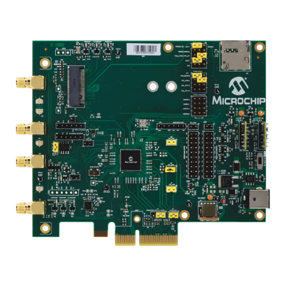
- Page 13 FIGURE 3-1: EVB-PCI11101 REV B (TOP-SIDE) 3.1.1 Power Input Options This EVB-PCI11101 is intended to be powered from one (1) external +12 VDC power supply connection: 1. J4 – AC/DC barrel jack 2023-2024 Microchip Technology Inc. and its subsidiaries...
- Page 14 EVB-PCI11101 Evaluation Kit User’s Guide 3.1.2 Power Mode Select Switch The EVB-PCI11101 has a Power Mode Select switch SW1 with two (2) modes, which must be chosen prior to applying power to the board. See Table 3-1. TABLE 3-1: POWER MODE SELECT OPTIONS...
- Page 15 When the EVB-PCI11101 is reset via J10 during runtime operation, the PCIe-depen- dent functions of the PCI11101 are not expected to function normally afterwards. Reset of EVB-PCI11101 shall normally occur prior to PCIe enumeration, as the EVB- PCI11101’s on-board 3.3V voltage regulator output becomes stable.
- Page 16 C EEPROM Install Install [1-2] to connect 3.3V power to the I VCC Power [1-2] EEPROM device. Enable Open [1-2] in order to disconnect 3.3V power to the I C EEPROM device. 2023-2024 Microchip Technology Inc.and its subsidiaries DS50003595B-page 16...
- Page 17 PCI11101) Open [1-2] to operate PCI11101 in normal, non- Test mode with JTAG TAP disabled. PCIe PRSNT# Install Install [1-2] to identify the EVB-PCI11101 as a 4- Lane Width Selec- [1-2] lane/x4 add-in-card. tion Install [2-3] to identify the EVB-PCI11101 as a 1- lane/x1 add-in-card.
- Page 18 Reset until [10-11] is populated instead. Install [13-14] to enable a pull up resistor on the m.2 DPR signal. Install [14-15] to enable a pull down resistor on the m.2 DPR signal. 2023-2024 Microchip Technology Inc.and its subsidiaries DS50003595B-page 18...
- Page 19 0.25m to 0.5m PCIe riser cable is strongly recommended to be connected between connector P1 and the upstream platform's PCIe add-in-card slot. The upstream platform's 12V and 3.3V power rails are routed to the EVB-PCI11101 via this P1 connector. However, EVB-PCI11101 is designed not to substantially load these power rails as it includes options for external 12V power supplies to become “self-pow-...
- Page 20 M.2 connector to an external antenna for greater signal integrity. 3.1.5.7 J34 – SIM CONNECTOR This connector allows external SIM cards to be connected to the EVB-PCI11101. This SIM connector is electrically connected to J29, allowing the use of LTE and 5G radio modules that require a SIM card.
- Page 21 Controller bus of PCI11101. This bus will only be enabled when J31 PCI11101 Config- uration Straps are configured to assert the CONFIG_EEPROM setting. (See J31 in Section 3.1.4 “Jumper Settings and Defaults”.) Refer to Figure 3-4. 2023-2024 Microchip Technology Inc. and its subsidiaries DS50003595B-page 21...
- Page 22 The majority of programmable pins available in PCI11101 are exposed across two pro- grammable pin probe headers to facilitate signal measurement and testing of non- default-use cases of EVB-PCI11101. Each programmable pin position is labeled in silk- screen adjacent to its probe pin, e.g. “P2” is for probing pin “PROG2”. See Table 3-3.
- Page 23 Pin 8 PROG77 Pin 9 PROG64 Pin 10 PROG78 Pin 11 PROG65 Pin 12 PROG79 Pin 13 PROG68 Pin 14 PROG80 Pin 15 PROG69 Pin 16 PROG81 Pin 17 PROG70 2023-2024 Microchip Technology Inc. and its subsidiaries DS50003595B-page 23...
- Page 24 PROG82 Pin 19 PROG71 Pin 20 PROG83 3.1.6 Evaluation Board LED Indicators Table 3-5 describes the LED indicators included on the EVB-PCI11101. TABLE 3-5: LED INDICATOR DESCRIPTIONS Reference Signal Name Description RESET# Lit when PCI11101 Reset pin is asserted. 12VIN_SW Lit when there is voltage present upon one of the 12V input power connectors.
- Page 25 U6, which inputs to M.2 add in card at J29 (dif- ferential) Ground reference near P1 TP16 Ground reference near J31 TP17 Ground reference near U22 TP18 Ground reference near J13 2023-2024 Microchip Technology Inc. and its subsidiaries DS50003595B-page 25...
- Page 26 EVB-PCI11101 Evaluation Kit User’s Guide NOTES: 2023-2024 Microchip Technology Inc.and its subsidiaries DS50003595B-page 26...
- Page 27 EVB-PCI11101 EVALUATION KIT USER’S GUIDE Appendix A. Schematics INTRODUCTION This appendix shows the EVB-PCI11101 Evaluation Kit Schematics. 2023-2024 Microchip Technology Inc. and its subsidiaries DS50003595B-page 27...
- Page 28 FIGURE A-1: EVB-PCI11101 BOARD POWER AND RESETS Board Power & Resets 3.3VDC to 1.8VDC Power Inputs, Switch and Voltage Regulators 1V8_BRD 1.8V @ 3A 1V8_BRD 3V3_BRD TP LOOP Orange 10-10488 TP13 Note: 12V ATX supply (12V_PCIE) can range 11.4-12.6V C102...
- Page 29 FIGURE A-2: PCI11101 POWER PCI11101 Power 1V1_BRD Place at J14[1-2] 3V3_BRD 1V8_BRD Place at J7[1-2] Place at J18[1-2] 1V1_ASIC Jumper Default: [1-2] 3V3_ASIC 1V8_ASIC Jumper Default: [1-2] Jumper Default: [1-2] 3V3_ASIC VDD11PA 0.1uF 1000pF 1000pF VDD11PA VDD33A0 VDD11PA VDD33A1 VDD11PA 0.1uF 1000pF 1000pF...
- Page 30 FIGURE A-3: PCI11101 I/O PCI11101 I/O 3.3V PCI11101 PROG0_EE_MST_SCL PROG0_EE_MST_SCL PCIE_RX_L0_P0_N PCIE_TXC_L0_P1_N 0.1uF PCIE_TX_L0_P1_N PROG1_EE_MST_SDA PCIE_RX_L0_P0_N PCIE_RXM_L0_P0 PCIE_TXM_L0_P1 PCIE_TX_L0_P1_N PROG1_EE_MST_SDA PROG0 0.1uF PCIE_RX_L0_P0_P PCIE_TXC_L0_P1_P PCIE_TX_L0_P1_P PROG2_SLV_ALERT_N PCIE_RX_L0_P0_P PCIE_RXP_L0_P0 PCIE_TXP_L0_P1 PCIE_TX_L0_P1_P PROG2_SLV_ALERT_N PROG1 0.1uF PCIE_TX_L0_P0_N PCIE_TXC_L0_P0_N PCIE_RX_L0_P1_N PROG4_PCIE_CLKREQ0_N PCIE_TX_L0_P0_N PCIE_TXM_L0_P0 PCIE_RXM_L0_P1 PCIE_RX_L0_P1_N 2, 5, 6 PROG4_PCIE_CLKREQ0_N...
- Page 31 FIGURE A-4: CONFIGURATION INTERFACES AND I/O BREAKOUTS Configuration Interfaces and I/O Breakouts Configuration via SMBus/SPI 3V3_BRD PROG Probe Place at J31[1-2] Place at J31[5-6] CFG_EEPROM PCI11101 Configuration Straps R131 R138 R140 R142 CFG_SERIAL PROG4_PCIE_CLKREQ0_N PROG30 2, 4, 6 PROG4_PCIE_CLKREQ0_N PROG30 SCL_CFG PU PROG5_PCIE_WAKE_N PROG31...
- Page 32 FIGURE A-5: PCIE UPSTREAM PORT PCIe Upstream Port Swapped P with N on the following to improve routing: PCIE_TX_L3_P0 PCIE_RX_L3_P0 PCIE_RX_L1_P0 PCIE TX L1 P0 12V_PCIE Note: this board does not support WAKE from D3_cold C125 PRSNT1_A1_N C126 nPRSNT1 Install this 0R set for optional JTAG connectivity 0.1uF 22uF See: "Configuration Interfaces and I/O Breakouts"...
- Page 33 FIGURE A-6: PCI11101 M.2 PCI11101 M.2 Control Header Config pull ups/pull downs SUSCLK oscillator 1V8_BRD 3V3_BRD 3V3_BRD From M.2 spec: Suspend Clock is a 32.768 kHz M.2 Control clock supply input that is provided by Platform PINMUX_AUTO PINMUX_SEL to enable the Adapter to enter reduce power Place at J35[1-2] PU ←...
- Page 34 EVB-PCI11101 Evaluation Kit User’s Guide NOTES: 2023-2024 Microchip Technology Inc.and its subsidiaries DS50003595B-page 34...
- Page 35 EVB-PCI11101 EVALUATION KIT USER’S GUIDE Appendix B. Bill of Materials INTRODUCTION This appendix contains the EVB-PCI11101 Evaluation Kit Bill of Materials. 2023-2024 Microchip Technology Inc. and its subsidiaries DS50003595B-page 35...
- Page 36 TABLE B-1: BILL OF MATERIALS (INSTALLED COMPONENTS) Item Qty. Reference Description Manufacturer Manufacturer Part Number C1, C2, C3, C4, C9, C51, C52, C54, C55, CAP CER 0.1uF 35V 10% X7R SMD 0402 TDK Corporation CGA2B3X7R1V104K050BB C56, C57, C58, C64, C66, C67, C75, C76, C77, C80, C81, C85, C86, C91, C93, C98, C99, C100, C101, C103, C108, C112, C116, C129, C133, C136, C137, C141,...
- Page 37 TABLE B-1: BILL OF MATERIALS (INSTALLED COMPONENTS) Item Qty. Reference Description Manufacturer Manufacturer Part Number C201, C202, C204, C206, C207, C208 CAP CER 0.1uF 35V 10% X7R SMD 0402 TDK Corporation CGA2B3X7R1V104K050BB D1, D2, D3 DIO LED GREEN 2V 30mA 35mcd Clear SMD 0603 Lite-On Inc LTST-C191KGKT D4, D6, D7, D8, D9, D11, D12, D13, D14,...
- Page 38 TABLE B-1: BILL OF MATERIALS (INSTALLED COMPONENTS) Item Qty. Reference Description Manufacturer Manufacturer Part Number TRANS FET P-CH SI4435 30V 12.6A 4.8W 0.019R SOIC-8 Vishay / Siliconix SI4435FDY-T1-GE3 Q2, Q5, Q7, Q10, Q11, Q12, Q13 TRANS FET N-CH 2N7002-7-F 60V 170mA 370mW SOT-23-3 Diodes Inc 2N7002-7-F TRANS BJT NPN MMBT3904 40V 200mA 310mW SOT-23-3...
- Page 39 TABLE B-1: BILL OF MATERIALS (INSTALLED COMPONENTS) Item Qty. Reference Description Manufacturer Manufacturer Part Number RES TF 8.98k 0.5% 1/10W SMD 0603 AEC-Q200 KOA Speer RN73R1JTTD8981D100 RES TKF 2.7k 1% 1/10W SMD 0603 Panasonic ERJ-3EKF2701V R78, R104, R109, R126 RES TF 10k 1% 1/10W SMD 0402 AEC-Q200 Vishay Beyschlag MCS0402MC1002FE000 RES TKF 200R 1% 1/10W SMD 0603 AEC-Q200...
- Page 40 Item Qty. Reference Description Manufacturer Manufacturer Part Number MCHP INTERFACE USB TYPE-C PORT PROTECT UCS4002 QFN-20 AECQ100 Microchip Technology UCS4002-E/6N U2, U3 MCHP INTERFACE USB PWR Controller with Auto Discharge UCS2113-1C-V/G4 Microchip Technology UCS2113-1C-V/G4 QFN-20 MCHP INTERFACE KSZ9131RNX 10/100/1000BASE-T QFN-48...
- Page 41 TABLE B-3: BILL OF MATERIALS (DO-NOT-POPULATE COMPONENTS) Item Qty. Reference Description Manufacturer Manufacturer Part Number BKT1 PCI Bracket, Global G5452 Global BRK1 MECH HW MISC PCIe Board Retainer Amfeltec Corporation SKU-038-01 C32, C34 CAP CER 15pF 5% 50V C0G/NP0 SMD 0402 AEC-Q200 Murata Electronics North America GCM1555C1H150JA16D C41, C131...
- Page 42 EVB-PCI11101 Evaluation Kit User’s Guide NOTES: 2023-2024 Microchip Technology Inc.and its subsidiaries DS50003595B-page 42...
- Page 43 EVB-PCI11101 EVALUATION KIT USER’S GUIDE Appendix C. PCB Silk Screens INTRODUCTION This appendix shows the top and bottom silk screens and 3D model images of the EVB-PCI11101. 2023-2024 Microchip Technology Inc. and its subsidiaries DS50003595B-page 43...
- Page 44 FIGURE C-1: EVB-PCI11101 TOP SILK SCREEN IMAGE...
- Page 45 FIGURE C-2: EVB-PCI11101 BOTTOM SILK SCREEN IMAGE...
- Page 46 Tel: 46-31-704-60-40 Tel: 631-435-6000 Sweden - Stockholm San Jose, CA Tel: 46-8-5090-4654 Tel: 408-735-9110 UK - Wokingham Tel: 408-436-4270 Tel: 44-118-921-5800 Canada - Toronto Fax: 44-118-921-5820 Tel: 905-695-1980 Fax: 905-695-2078 2023-2024 Microchip Technology Inc. and its subsidiaries DS50003595B-page 46 04/15/24...
Need help?
Do you have a question about the EVB-PCI11101 and is the answer not in the manual?
Questions and answers