
Related Manuals for Microchip Technology EVB-LAN9696-24port


Summary of Contents for Microchip Technology EVB-LAN9696-24port
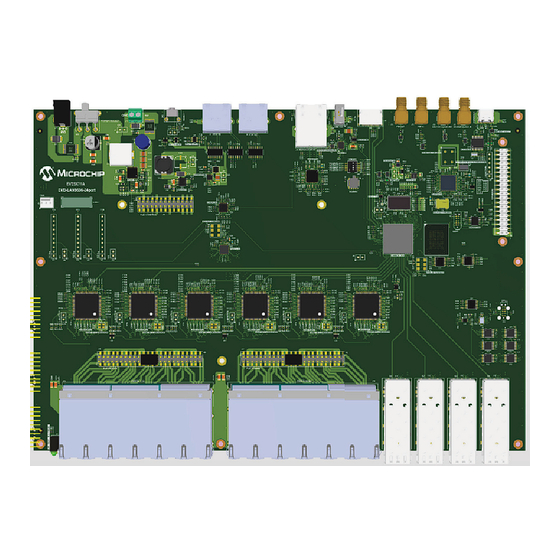
- Page 1 EVB-LAN9696-24port Hardware Manual 2024 Microchip Technology Inc. and its subsidiaries DS50003657A...
- Page 2 The Adaptec logo, Frequency on Demand, Silicon Storage Technology, and Symmcom are registered trademarks of Microchip Technology Inc. in other countries. GestIC is a registered trademark of Microchip Technology Germany II GmbH & Co. KG, a subsidiary of Microchip Technology Inc., in other countries. All other trademarks mentioned herein are property of their respective companies.
-
Page 3: Table Of Contents
4.2 Rear-side Layout ..................28 ® 4.2.1 USB Type-C Serial Port ................28 4.2.2 SMA Connectors ..................28 4.2.3 PCIe 2.0 – Oculink Connector ..............28 4.2.4 ULPI USB 2.0 Host ..................28 2024 Microchip Technology Inc. and its subsidiaries DS50003657A-page 3... - Page 4 5.5 Reference Clocks, Synchronization, and PTP ..........49 5.5.1 Switch and CuPHY Reference Clocks ............49 5.5.2 Sync-E and PTP Generated Reference Clocks .........50 5.5.3 SMA Connectors ..................51 5.6 Ultra PoE Feature Connectors ..............52 2024 Microchip Technology Inc. and its subsidiaries DS50003657A-page 4...
- Page 5 A.2.11 DDR4 Close-up on Signal Plane 2 ............66 A.2.12 DDR4 Close-up on Bottom Layer ............66 A.3 PCB Layer Stack-up ..................67 A.3.1 PCB trace Widths, Clearance, and Impedance ......... 67 Worldwide Sales and Service ..................70 2024 Microchip Technology Inc. and its subsidiaries DS50003657A-page 5...
- Page 6 EVB-LAN9696-24port Hardware Manual NOTES: 2024 Microchip Technology Inc. and its subsidiaries DS50003657A-page 6...
-
Page 7: Preface
Select the Help menu, and then Topics to open a list of available online help files. INTRODUCTION This chapter contains general information that will be useful to know before using the EVB-LAN9696-24port Hardware Manual. Items discussed in this chapter include: • Document Layout •... - Page 8 Choice of mutually exclusive errorlevel {0|1} character: { | } arguments; an OR selection Ellipses... Replaces repeated text var_name [, var_name...] Represents code supplied by void main (void) user { ... 2024 Microchip Technology Inc. and its subsidiaries DS50003657A-page 8...
- Page 9 MPLAB REAL ICE in-circuit emulator, MPLAB ICD 3 in-circuit debugger and MPLAB PM3 device programmers. Also included are nonproduction development programmers such as PICSTART Plus and PIC-kit 2 and 3. 2024 Microchip Technology Inc. and its subsidiaries DS50003657A-page 9...
- Page 10 Technical support is available through the web site at: http://www.microchip.com/support DOCUMENT REVISION HISTORY Revisions Section/Figure/Entry Correction DS50003657A Initial release (02-23-24) 2024 Microchip Technology Inc. and its subsidiaries DS50003657A-page 10...
-
Page 11: Chapter 1. Overview
• IEEE802.1Q, Virtual Bridged Local Area Networks • IEEE802.3, CSMA/CD Access Method and Physical Layer Specification • IEEE1588-2019, Precision Clock Synchronization Protocol 1.3.3 (Optical) Module Standards • SFP+ MSA, ftp://ftp.seagate.com/sff/SFF-8431.PDF 2024 Microchip Technology Inc. and its subsidiaries DS50003657A-page 11... -
Page 12: Acronyms And Definitions
Small Form-factor Pluggable transceiver SFP+ Small Form-factor Pluggable transceiver for 10 Gbps Serial Interface (SPI) Small/Medium Enterprise Synchronization Status Message Sync-E Synchronous Ethernet (ITU-T G.8262/Y.1362) TF-A Trusted Firmware for ARM Two-wired Interface 2024 Microchip Technology Inc. and its subsidiaries DS50003657A-page 12... -
Page 13: Chapter 2. Evb-Lan9696 Reference Board
• Option for external CPU control via SPI and PCIe • Expansion header - Raspberry Pi compatibility regarding power, UART, and I • Barrel jack for 12V DC power and screw terminal for 48V/56V DC power. 2024 Microchip Technology Inc. and its subsidiaries DS50003657A-page 13... -
Page 14: Board Design
The SPI client is set up through a specific boot mode. The PCIe end-point can either be set up through the SPI client or from a QSPI boot NOR Flash device. 2024 Microchip Technology Inc. and its subsidiaries DS50003657A-page 14... -
Page 15: Management
10G ports on LAN9696 or from one of the CuPHY ports. The board uses the LAN8814 CuPHY’s capability to daisy-chain recovered PHY clocks and preselect which two clocks would be presented to the on-board DPLL, as shown Figure 2-2. 2024 Microchip Technology Inc. and its subsidiaries DS50003657A-page 15... -
Page 16: Ptp/Ieee1588V2/802.1As-2020
12V power. The 12V power sources a number of local DC/DC converters, the FAN con- nector and the PoE header. Table 2-1 shows how the r power supplies are generated and used on the board. 2024 Microchip Technology Inc. and its subsidiaries DS50003657A-page 16... - Page 17 1.2V by MIC23050. LAN9696 VDDIO_DDR and DDR4 VDDQ 1.8V by MIC23303. LAN9696: VDDIO, VDDH, VDDPLLDDR ZL80732B: Core. 3.3V 2.5V by MIC5377. DDR4 The expansion header can supply both 5V and 3.3V power. 2024 Microchip Technology Inc. and its subsidiaries DS50003657A-page 17...
- Page 18 EVB-LAN9696-24port Hardware Manual NOTES: 2024 Microchip Technology Inc. and its subsidiaries DS50003657A-page 18...
-
Page 19: Chapter 3. Management Software
IP address where the Web GUI is available. An example of the CLI output when setting up a Static Aggregation on the 4x 10G ports is shown in Figure 3-1. 2024 Microchip Technology Inc. and its subsidiaries DS50003657A-page 19... -
Page 20: Web Gui For Management
Switch Application can be uploaded through the Maintenance tab. Help screens are available through the “?” button at top right. Figure 3-3 shows an example Web GUI screenshot of the status of the previous Aggre- gation setup. 2024 Microchip Technology Inc. and its subsidiaries DS50003657A-page 20... -
Page 21: Firmware Update Using Tf-A
4. Use either Chrome or MS Edge browser and have the browser setting, JavaS- cript, enabled. Simply run the fwu.html file inside the browser address field. 5. Click on the Connect device button. (See Figure 3-4.) The dialogue in Figure 3-5 appears. 2024 Microchip Technology Inc. and its subsidiaries DS50003657A-page 21... - Page 22 EVB-LAN9696-24port Hardware Manual FIGURE 3-4: CONNECTING TO LAN9696 FIRMWARE TOOL 6. Select MCP2200 and click on Connect. FIGURE 3-5: COM PORT SELECTION 2024 Microchip Technology Inc. and its subsidiaries DS50003657A-page 22...
- Page 23 11. When done, select the next tab, Write Image, and choose eMMC as shown in Figure 3-9. Click on Write Flash Image. The Flash programming will take about 20 seconds. 2024 Microchip Technology Inc. and its subsidiaries DS50003657A-page 23...
- Page 24 INITIAL EMMC BOOT LOG 14. Recommended step: Run the following commands to have the U-Boot environ- ment match the current U-Boot version: m => env default -a m => saveenv m => reset 2024 Microchip Technology Inc. and its subsidiaries DS50003657A-page 24...
- Page 25 MMC write: dev # 0, block # 534528, count 262144 ... 262144 blocks written: OK success! MMC write: dev # 0, block # 2631680, count 262144 ... 262144 blocks written: OK m => 2024 Microchip Technology Inc. and its subsidiaries DS50003657A-page 25...
-
Page 26: Using Firmware Update To Upload Pcie ® Driver
The Firmware update utility can be used to upload a special LAN969x_PCIe image to the NOR Flash. The image configures and enables the PCIe end-point interface. The bin file does not contain U-boot. The LAN969x_PCIe image is released along with the TFA software. 2024 Microchip Technology Inc. and its subsidiaries DS50003657A-page 26... -
Page 27: Chapter 4. Led Indicators And Board Connector
Switch serial GPIO engine. The SFP I C required clock muxing is made by using an (external) 8-channel analog multiplexer. Three select pins are controlled through the Switch serial GPIO engine. 2024 Microchip Technology Inc. and its subsidiaries DS50003657A-page 27... -
Page 28: Rear-Side Layout
FET switch provides the 5V_host sourcing, limited to 600 mA. The actual host capabilities depend on the Linux OS system support – though an USB memory key has been tested. 2024 Microchip Technology Inc. and its subsidiaries DS50003657A-page 28... -
Page 29: Management Port And Status Led
The Expansion header is partially compatible with Raspberry Pi. GNSS modules (designed for RPI) can be mounted to provide GNSS time input to the system using UART and 1PPS signals. 2024 Microchip Technology Inc. and its subsidiaries DS50003657A-page 29... -
Page 30: Ultra Poe Connector
A/D converter for monitoring it through the register interface. 4.3.7 FAN Connector A FAN connector, J31, is available next to the left edge of an attached PoE add-on PCB. 2024 Microchip Technology Inc. and its subsidiaries DS50003657A-page 30... -
Page 31: Boot Mode And Reference Clock
System default is to boot from the on-board eMMC NAND Flash device. Additionally, it is possible to strap the source to the core reference clock through REF- CLK_SEL. As a default, the differential 156.25 MHz clock input is selected. 2024 Microchip Technology Inc. and its subsidiaries DS50003657A-page 31... - Page 32 EVB-LAN9696-24port Hardware Manual NOTES: 2024 Microchip Technology Inc. and its subsidiaries DS50003657A-page 32...
-
Page 33: Chapter 5. Detailed Hardware Description
TCXO type, a clock recovered from one of the 10G SerDes ports on LAN9696 or by one of the on-board CuPHY’s. A recovered clock-chain links all the LAN8814 PHYs for pre-selection of the recovered clock source(s). 2024 Microchip Technology Inc. and its subsidiaries DS50003657A-page 33... -
Page 34: Vcore-Iv Cpu Sub-System
25 MHz reference clock in IEEE 1588 applications to separate the Sync-E and PTP timing domains. 2024 Microchip Technology Inc. and its subsidiaries DS50003657A-page 34... -
Page 35: Ddr4 Sdram
FIGURE 5-2: TC2020-NL-FP FOOTPRINT AND ASSOCIATED PROBE The probe used with TC2050-NL-FP can be brought from Tag-connect.com homepage: https://www.tag-connect.com/product/tc2050-nl-fp-footprint 2024 Microchip Technology Inc. and its subsidiaries DS50003657A-page 35... -
Page 36: Arm Cpu Jtag Header
Table 5-4 shows which tap controller can be selected. Default mode is CPU Tap controller. TABLE 5-4: JTAG MODE OF OPERATION JTAG_SEL Mode Test Tap controller CPU Tap controller 2024 Microchip Technology Inc. and its subsidiaries DS50003657A-page 36... -
Page 37: Flexcom Usage
USB-TO-UART SERIAL CONVERSION ® The USB converter is locally powered through its USB Type-C connector using a low dropout (LDO) voltage regulator, MCP1700. It awakes smoothly, when connected to a Host USB. 2024 Microchip Technology Inc. and its subsidiaries DS50003657A-page 37... -
Page 38: Uart For Ieee 1588 Time Interface - Rj45 G.703 Pinout
FLEXCOM2 SPI host interface is being used to control the on-board DPLL. This serial interface consists of the usual signals SPI clock DPLL.SCK (SCLK), data out DPLL.STX (MOSI), data in DPLL.SRX (MISO), and chipselect DPLL.nCS (nCS). 2024 Microchip Technology Inc. and its subsidiaries DS50003657A-page 38... -
Page 39: I 2 C Interface
The LAN9696 built-in USB Host controller is connected to a Hi-Speed USB 2.0 trans- ceiver PHY, USB3343 through its ULPI port interface located on the Switch GPIO in alternate mode. Figure 5-5 shows how the external transceiver PHY has been implemented. 2024 Microchip Technology Inc. and its subsidiaries DS50003657A-page 39... -
Page 40: Serial Gpio Controller
PLD and individual endpoints. By using shift reg- isters, only the four LAN9696 Serial GPIO signals need to be routed “long distance” as each shift register can be distributed across the board as applicable. 2024 Microchip Technology Inc. and its subsidiaries DS50003657A-page 40... - Page 41 S7.TXFAULT (1=TX fault on SFP) S7.TXDIS p7b3 — S7.RATESEL (RS1 and RS2) p8b0 S8.LOS (1=LOS from SFP) S8.LED1 – Green p8b1 S8.MODDET (0=SFP present) S8.LED2 – Red p8b2 S8.TXFAULT (1=TX fault on SFP) S8.TXDIS 2024 Microchip Technology Inc. and its subsidiaries DS50003657A-page 41...
-
Page 42: Mii-Management Bus Interface
By using LAN9696 built-in FAN controller, the FAN speed is adjustable through “ground chopping” with a PWM-controlled FET. FAN “health” is monitored through the LAN9696 tacho input. Table 5-10 describes the FAN pin header. 2024 Microchip Technology Inc. and its subsidiaries DS50003657A-page 42... -
Page 43: Lan9696 Gpio Usage
FC0.TXD ALT1 SGPIO.CK Serial GPIO controller 0 ALT1 SGPIO.LD ALT1 SGPIO.DO ALT1 SGPIO.DI ALT1 MII-Management controller 0 ALT1 MDIO ALT1 MDINTn ALT3 USB.nRESET USB Host PHY Reset output - RESETB 2024 Microchip Technology Inc. and its subsidiaries DS50003657A-page 43... - Page 44 TX_CLK RGMII0 TX_CTL ALT1 SE.RC1 Sync-E Recovered Clock 1 output to DPLL ALT2 FC3.SCL FLEXCOM3 TWIHS – I C for various use ALT2 FC3.SDA ALT4 PTP.SYNC3 1PPS output to PHY’s 2024 Microchip Technology Inc. and its subsidiaries DS50003657A-page 44...
-
Page 45: Switch Core
PCIe PCIE PCIe end-point controller 5.3.2 Copper PHYs 5.3.2.1 MEDIA SIDE INTERFACE The twisted pair interface on the copper PHYs are fully compliant with the IEEE802.3-2005 specification for CAT-5 media. 2024 Microchip Technology Inc. and its subsidiaries DS50003657A-page 45... -
Page 46: Integrated
MODE_SEL0=1, ‘11001’ = ANEG and AMDIX. 1588_REF_CLK DPLL clock output 1588_LD_ADJ MODE_SEL1=0. 1PPS input from LAN9668 or DPLL. only strapped MODE_SEL2=0 only strapped MODE_SEL3=1 only strapped MODE_SEL4=1 RCVRD_CKI1x RCVRD_CK_IN1 RCVRD_CKI2x RCVRD_CK_IN2 RCVRD_CKO1x RCVRD_CK_OUT1 2024 Microchip Technology Inc. and its subsidiaries DS50003657A-page 46... -
Page 47: Sfp+, Sfi Interfaces
The PCIe end-point does support frame injection and extraction. The maximum possible bandwidth to obtain somehow depends on the ‘horsepower’ of the external CPU system. Note: The LAN9696 PCIe interface cannot operate as host/root-complex. 2024 Microchip Technology Inc. and its subsidiaries DS50003657A-page 47... -
Page 48: Reset Circuitry
SET_3V is asserted, when the sense voltage drops below the threshold, 0.4V, or when nCLKRESET is pulled low. The active-low Reset stays low for the duration of the Reset timeout delay once the sense voltage returns to normal and the manual Reset transi- 2024 Microchip Technology Inc. and its subsidiaries DS50003657A-page 48... -
Page 49: Reference Clocks, Synchronization, And Ptp
Recovered clocks, CuPHY 1588 and 1PPS clocks are distributed as single-ended clocks. A single-ended clock buffer, like ZL40241 typically offers a cost advantage com- pared to a differential clock buffer. 2024 Microchip Technology Inc. and its subsidiaries DS50003657A-page 49... -
Page 50: Sync-E And Ptp Generated Reference Clocks
25 MHz recovered clock from CuPHY (RCLK_PHY1) REF1P 25 MHz recovered clock from Switch (RCLK_SW/SE_RC0) REF1N 25 MHz Sync-E feedback from OUT2N (RCLK_DPLL) REF2P 10 MHz station clock input from SMA (CKSTATION_I)/J11 2024 Microchip Technology Inc. and its subsidiaries DS50003657A-page 50... -
Page 51: Sma Connectors
1.544 or 2.048 MHz, this can be controlled by the running Switch Application. TABLE 5-16: SMA CONNECTORS SMA name Connector Description STATION CLOCK SyncE clock to board DPLL/REF2P. AC coupled. STATION CLOCK SyncE clock from board DPLL/OUT1P. AC coupled. 2024 Microchip Technology Inc. and its subsidiaries DS50003657A-page 51... -
Page 52: Ultra Poe Feature Connectors
VP_N_U5/U17 VP_N6/N18 VP_N_U6/U18 VP_PMA VP_PMA VP_PMA VP_PMA VP_N7/N19 VP_N_U7/U19 VP_N8/N20 VP_N_U8/U20 VP_PMA VP_PMA VP_PMA VP_PMA VP_N9/N21 VP_N_U9/U21 VP_N10/N22 VP_N_U10/U22 VP_PMA VP_PMA VP_PMA VP_PMA Note 1: Maximum current VP_Nx is 1A. 2024 Microchip Technology Inc. and its subsidiaries DS50003657A-page 52... -
Page 53: Expansion Header
2X20-PIN EXPANSION HEADER, J4 Signal Direction Direction Signal 3.3V I2C SDA (FLEXCOM3) BiDir I2C SCL (gated SEL=7) Spare UART TXD (FLEXCOM1) UART RXD (FLEXCOM1) Spare PTP_IN (SYNCE5) (1PPS) Spare Spare Spare 2024 Microchip Technology Inc. and its subsidiaries DS50003657A-page 53... -
Page 54: Power Distribution
• 3V3 for SFP and CuPHY’s IO and analog high. The calculated load is 4.8A. Maxi- mum current is 6A. • 5V for USB Host and additional DC/DC converters.The calculated load is 1.2A. Maximum current is 2A. 2024 Microchip Technology Inc. and its subsidiaries DS50003657A-page 54... - Page 55 LAN8814/LAN8840 VDDIO and Analog High ZL80732B and ZL40217 VDD. OCXO USB Host PHY and Shift Registers — — SFP+ Slot Expansion Header and PoE Headers — — Total 3.3V 15.8 power usage. 2024 Microchip Technology Inc. and its subsidiaries DS50003657A-page 55...
-
Page 56: Power Supply Sequencing
A two-pin footprint can be found on each power supply output. • 56V: J19 • 12V: J21 • 5V: J24 • 3V3: J22 • 2V5: TP21 • 1V8: J26 • 1V2: J27 • 1V1: J20 • 0V9: J25 2024 Microchip Technology Inc. and its subsidiaries DS50003657A-page 56... -
Page 57: Chapter 6. Environmental Requirements
• Operating humidity: 10% to 95% relative humidity, non-condensing The reference board is provided without a case, so sufficient airflow might be needed, if the air temperature is above 30°C. 2024 Microchip Technology Inc. and its subsidiaries DS50003657A-page 57... - Page 58 EVB-LAN9696-24port Hardware Manual NOTES: 2024 Microchip Technology Inc. and its subsidiaries DS50003657A-page 58...
-
Page 59: Appendix A. Pcb Layout
(The outer layers do not have ground fill areas for copper balancing purposes.) 2024 Microchip Technology Inc. and its subsidiaries DS50003657A-page 59... -
Page 60: Layer 1 - Top Plane
Layer 1 - Top Plane FIGURE A-2: LAYER 1 - TOP PLANE Mostly signal traces for DDR4 and SerDes Tx Macros. 12V and 48V/56V input power and PoE center tap power distribution. 2024 Microchip Technology Inc. and its subsidiaries DS50003657A-page 60... -
Page 61: Layer 2 - Ground Plane
LAYER 2 - GROUND PLANE Solid ground plane. A.2.3 Layer 3 FIGURE A-4: LAYER 3 - SIGNAL PLANE 1 Signal traces for DDR4L. Various clocks for CuPHYs and Switch. SFP control signals. 2024 Microchip Technology Inc. and its subsidiaries DS50003657A-page 61... -
Page 62: Layer 4
LAYER 5 - POWER PLANE 2 3V3U Power planes; mainly the 3V3. The 1V1 is made ‘short and wide’ as possible. DDR4L 1V2 and VTT power plane. 5V Host and USB power planes. 2024 Microchip Technology Inc. and its subsidiaries DS50003657A-page 62... -
Page 63: Layer 6 - Signal Plane 2
The plane is the SFP shield ground. Signal traces for DDR4, RGMII to Single PHY. ULPI host interface. A.2.7 Layer 7 - Ground Plane 2 FIGURE A-8: LAYER 7 - GROUND PLANE 2 Solid ground plane. 2024 Microchip Technology Inc. and its subsidiaries DS50003657A-page 63... -
Page 64: Layer 8
EVB-LAN9696-24port Hardware Manual A.2.8 Layer 8 FIGURE A-9: LAYER 8 - BOTTOM PLANE Signal traces for DDR4L and SerDes Rx macros. Copper PHY MDI 2024 Microchip Technology Inc. and its subsidiaries DS50003657A-page 64... -
Page 65: Ddr4 Close-Up On Top Layer
DDR4 in close-up to illustrate how the DDR length matching is acquired. FIGURE A-10: DDR CLOSE-UP ON TOP LAYER A.2.10 DDR4 Close-up on Signal Plane 1 FIGURE A-11: DDR CLOSE UP ON SIGNAL PLANE 1 2024 Microchip Technology Inc. and its subsidiaries DS50003657A-page 65... -
Page 66: Ddr4 Close-Up On Signal Plane 2
DDR CLOSE-UP ON SIGNAL PLANE 2 A.2.12 DDR4 Close-up on Bottom Layer FIGURE A-13: DDR CLOSE-UP ON BOTTOM LAYER LAN9696 package skew report is available upon request. Contact your Microchip representative. 2024 Microchip Technology Inc. and its subsidiaries DS50003657A-page 66... -
Page 67: Pcb Layer Stack-Up
— — Dielectric 2 CR-FR408HR-28mil 12.00mil 3.7, 0.0088 — PWR2 CF-004 1.378mil — — — Dielectric 8 PP-FR408HR-1080_71 4.016mil 3.34, 0.01 — — Dielectric 6 PP-FR408HR-1080_71 4.016mil 3.34, 0.01 — 2024 Microchip Technology Inc. and its subsidiaries DS50003657A-page 67... - Page 68 DDR SE impedance 60Ω between devices. No impedance => 4 mil trace on any layer. Any unspecified nets should be routed as 60Ω. Critical clock nets: CLK156 - route with extra clearance. 2024 Microchip Technology Inc. and its subsidiaries DS50003657A-page 68...
- Page 69 PCB Layout NOTES: 2024 Microchip Technology Inc. and its subsidiaries DS50003657A-page 69...
-
Page 70: Worldwide Sales And Service
Tel: 46-31-704-60-40 Tel: 631-435-6000 Sweden - Stockholm San Jose, CA Tel: 46-8-5090-4654 Tel: 408-735-9110 UK - Wokingham Tel: 408-436-4270 Tel: 44-118-921-5800 Canada - Toronto Fax: 44-118-921-5820 Tel: 905-695-1980 Fax: 905-695-2078 2024 Microchip Technology Inc. and its subsidiaries DS50003657A-page 70 09/14/21...
Need help?
Do you have a question about the EVB-LAN9696-24port and is the answer not in the manual?
Questions and answers