Advertisement
ECLSOIC8EVB
Evaluation Board User's
Manual for High Frequency
SOIC 8
ON Semiconductor has developed an evaluation board for
the devices in 8−lead SOIC package. These evaluation
boards are offered as a convenience for the customers
interested in performing their own engineering assessment
on the general performance of the 8−lead SOIC device
samples. The board provides a high bandwidth 50 W
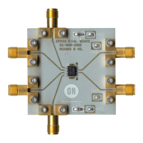
controlled impedance environment. The pictures in Figure 1
show the top and bottom view of the evaluation board, which
can be configured in several different ways, depending on
device under test (See Table 1. Configuration List).
This evaluation board manual contains:
•
Information on 8−lead SOIC Evaluation Board
•
Assembly Instructions
•
Appropriate Lab Setup
•
Bill of Materials
This manual should be used in conjunction with the device
data sheet, which contains full technical details on the device
specifications and operation.
© Semiconductor Components Industries, LLC, 2012
January, 2012 − Rev. 2
Arrow.com.
Downloaded from
INTRODUCTION
Figure 1. Top and Bottom View of the 8−lead SOIC Evaluation Board
http://onsemi.com
EVAL BOARD USER'S MANUAL
Board Lay−Up
The 8−lead SOIC evaluation board is implemented in four
layers with split (dual) power supplies (Figure 2.
Evaluation Board Lay−up). For standard ECL lab setup and
test, a split (dual) power supply is essential to enable the
50 W internal impedance in the oscilloscope as a termination
for ECL devices. The first layer or primary trace layer is
0.008" thick Rogers RO4003 material, which is designed to
have equal electrical length on all signal traces from the
device under the test (DUT) to the sense output. The second
layer is the 1.0 oz copper ground plane and a portion of the
plane is the V
power plane. The FR4 dielectric material is
EE
placed between second and third layer and between third and
fourth layer. The third layer is also 1.0 oz copper ground
plane and a portion of this layer is V
fourth layer is the secondary trace layer.
1
power plane. The
CC
Publication Order Number:
EVBUM2056/D
Advertisement
Table of Contents

Subscribe to Our Youtube Channel
Related Manuals for ON Semiconductor ECLSOIC8EVB


Summary of Contents for ON Semiconductor ECLSOIC8EVB
- Page 1 INTRODUCTION Board Lay−Up The 8−lead SOIC evaluation board is implemented in four ON Semiconductor has developed an evaluation board for layers with split (dual) power supplies (Figure 2. the devices in 8−lead SOIC package. These evaluation Evaluation Board Lay−up). For standard ECL lab setup and...
-
Page 2: Silkscreen (Top Side)
ECLSOIC8EVB LAY−UP DETAIL 4 LAYER SILKSCREEN (TOP SIDE) LAYER 1 (TOP SIDE) 0.062 $ 0.007 ROGERS 4003 0.008 in LAYER 2 (GROUND AND VEE PLANE P1) 1 OZ FR−4 0.020 in LAYER 3 (GROUND AND VCC PLANE P2) 1 OZ FR−4 0.025 in... - Page 3 ECLSOIC8EVB Table 1. Configuration List ECLinPS PlusE ECLinPS LiteE Device Comments Configuration Device Comments Configuration MC10EP01D/MC100EP01D See Figure 4 MC10EL01D/MC100EL01D See Figure 4 MC10EP05D/MC100EP05D See Figure 4 MC10EL04D/MC100EL04D See Figure 5 MC10EP08D/MC100EP08D See Figure 4 MC10EL05D/MC100EL05D See Figure 4 MC10EP11D/MC100EP11D...
- Page 4 ECLSOIC8EVB Evaluation Board Assembly Instructions On the top side of the evaluation board solder the four The 8−lead SOIC evaluation board is designed for surface mount test point clips to the pads labeled V characterizing devices in a 50 W laboratory environment and GND.
- Page 5 ECLSOIC8EVB CONFIGURATIONS 0.1 mF 50 W 0.01 mF 50 W 50 W 0.01 mF 50 W 0.1 mF Figure 4. Configuration 1 Schematic Table 4. Configuration 1 Pin 1 Pin 2 Pin 3 Pin 4 Pin 5 Pin 6 Pin 7...
- Page 6 ECLSOIC8EVB 0.1 mF Pin 1 Pin 8 0.01 mF Pin 7 Pin 2 50 W Pin 3 Pin 6 50 W 0.01 mF Pin 4 Pin 5 0.1 mF (Optional) Figure 5. Configuration 2 Schematic Table 5. Configuration 2 Pin 1...
- Page 7 ECLSOIC8EVB 0.1 mF Pin 1 Pin 8 0.01 mF Pin 7 Pin 2 50 W Pin 3 Pin 6 50 W 0.01 mF Pin 4 Pin 5 0.1 mF Figure 6. Configuration 3 Schematic Table 6. Configuration 3 Pin 1...
- Page 8 ECLSOIC8EVB 0.1 mF Pin 1 Pin 8 50 W 0.01 mF Pin 7 Pin 2 50 W Pin 3 Pin 6 50 W 0.01 mF Pin 4 Pin 5 0.1 mF (Optional) Figure 7. Configuration 4 Schematic Table 7. Configuration 4...
- Page 9 ECLSOIC8EVB 0.1 mF Pin 1 Pin 8 0.01 mF Pin 7 Pin 2 50 W Pin 3 Pin 6 50 W 0.01 mF Pin 4 Pin 5 50 W 0.1 mF (Optional) Figure 8. Configuration 5 Schematic Table 8. Configuration 5...
- Page 10 ECLSOIC8EVB 0.1 mF Pin 1 Pin 8 0.01 mF Pin 7 Pin 2 50 W (optional) J7 Pin 3 Pin 6 Pin 4 Pin 5 Short Figure 9. Configuration 6 − Translator Schematic Table 9. Configuration 6 Pin 1 Pin 2...
- Page 11 ECLSOIC8EVB 0.1 mF Pin 1 Pin 8 0.01 mF Pin 7 Pin 2 50 W Pin 3 Pin 6 50 W Pin 4 Pin 5 Short Figure 10. Configuration 7 − Translator Schematic (Unloaded Testing Condition) Table 10. Configuration 7...
- Page 12 ECLSOIC8EVB 0.1 mF Pin 1 Pin 8 0.01 mF Pin 7 Pin 2 50 W (optional) Pin 3 Pin 6 50 W (optional) Pin 4 Pin 5 Short Figure 11. Configuration 8 − Translator Schematic Table 11. Configuration 8 Pin 1...
- Page 13 ECLSOIC8EVB 0.1 mF Pin 1 Pin 8 50 W 0.01 mF Pin 7 Pin 2 50 W Pin 3 Pin 6 50 W Pin 4 Pin 5 Short 50 W Figure 12. Configuration 9 − Translator Schematic (Unloaded Testing Condition) Table 12.
- Page 14 ECLSOIC8EVB 0.1 mF Pin 1 Pin 8 0.01 mF Pin 7 Pin 2 50 W Pin 3 Pin 6 50 W Pin 4 Pin 5 Short Figure 13. Configuration 10 − Translator Schematic (Unloaded Testing Condition) Table 13. Configuration 10...
- Page 15 ECLSOIC8EVB 0.1 mF Pin 1 Pin 8 50 W 0.01 mF Pin 7 Pin 2 50 W Pin 3 Pin 6 50 W (optional) Pin 4 Pin 5 Short Figure 14. Configuration 11 − Translator Schematic Table 14. Configuration 11...
-
Page 16: Lab Setup
ECLSOIC8EVB LAB SETUP Power Supply OUT1 Test Measuring Equipment Channel 1 OUT1 Differential Signal Generator Channel 2 OUT2 OUT2 TRIGGER TRIGGER Power Supply Figure 15. Example of Standard Lab Setup (Configuration 1) 1. Connect appropriate power supplies to V The power supply for voltage level translating device need and GND. - Page 17 ECLSOIC8EVB Table 17. Bill of Materials Components Manufacturer Description Part Number Web Site SMA Connector Rosenberger SMA Connector, Side 32K243−40ME3 http://www.rosenberger.de Launch, Gold Plated http://www.rosenbergerna.com Johnson SMA Connector, Side 142−0701−851 http://www.johnsoncomponents.com Components* Launch, Gold Plated Surface Mount Test Keystone* SMT Miniature Test Point 5015 http://www.keyelco.com...
-
Page 18: Appendix A (Modified Configurations)
ECLSOIC8EVB Appendix A (Modified Configurations) MC100EP16VSD This device has an option of varying the output swing MC10EL16D/MC100EL16D amplitude and being driven single−endedly. In order to MC100LVEL16D utilize these options, Configuration 2 needs to be modified. MC10EP16D/MC100EP16D Output Swing Control MC10EP16DF/MC100EP16DF 1. -
Page 19: Appendix B (Gerber Files)
ECLSOIC8EVB Appendix B (Gerber Files) Top Layer Second Layer (V and Ground Plane Third Layer (V and Ground Plane) Bottom Layer Figure 16. Gerber Files ECLinPS, ECLinPS Lite, ECLinPS Plus, and ECLinPS MAX are trademarks of Semiconductor Components Industries, LLC (SCILLC). -
Page 20: Additional Information
onsemi, , and other names, marks, and brands are registered and/or common law trademarks of Semiconductor Components Industries, LLC dba “onsemi” or its affiliates and/or subsidiaries in the United States and/or other countries. onsemi owns the rights to a number of patents, trademarks, copyrights, trade secrets, and other intellectual property. A listing of onsemi’s product/patent coverage may be accessed at www.onsemi.com/site/pdf/Patent−Marking.pdf.
Need help?
Do you have a question about the ECLSOIC8EVB and is the answer not in the manual?
Questions and answers