Advertisement
Quick Links
ECLLQFP32EVB
Evaluation Board User's
Manual for High Frequency
LQFP32
INTRODUCTION
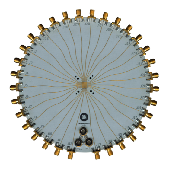
ON Semiconductor has developed an evaluation board
for the devices in 32−lead LQFP package. These evaluation
boards are offered as a convenience for the customers
interested in performing their own engineering assessment
on the general performance of the 32−lead LQFP device
samples. The board provides a high bandwidth 50 W
controlled impedance environment. Figures 1 and 2 show
the top and bottom view of the evaluation board, which can
be configured in several different ways, depending on
device under test (see Table 1. Configuration List).
This evaluation board manual contains:
•
Information on 32−lead LQFP Evaluation Board
•
Assembly Instructions
•
Appropriate Lab Setup
•
Bill of Materials
© Semiconductor Components Industries, LLC, 2012
January, 2012 − Rev. 3
Figure 1. Top View of the 32−lead LQFP Evaluation Board
EVAL BOARD USER'S MANUAL
This manual should be used in conjunction with the device
data sheet, which contains full technical details on the device
specifications and operation.
Board Lay−Up
The 32−lead LQFP evaluation board is implemented in
four layers with split (dual) power supplies (see Figure 3.
Evaluation Board Lay−Up). For standard ECL lab setup and
test, a split (dual) power supply is essential to enable the
50 W internal impedance in the oscilloscope as a termination
for ECL devices. The first layer or primary trace layer is
0.008" thick Rogers RO4003 material, which is designed to
have equal electrical length on all signal traces from the
device under the test (DUT) to the sense output. The second
layer is the 1.0 oz copper ground. The FR4 dielectric
material is placed between second and third layer and
between third and fourth layer. The third layer is the power
plane (V
and V
) and a portion of this layer is a ground
CC
EE
plane. The fourth layer is the secondary trace layer.
1
http://onsemi.com
Publication Order Number:
EVBUM2055/D
Advertisement

Related Manuals for ON Semiconductor ECLLQFP32EVB


Summary of Contents for ON Semiconductor ECLLQFP32EVB
- Page 1 INTRODUCTION This manual should be used in conjunction with the device data sheet, which contains full technical details on the device ON Semiconductor has developed an evaluation board specifications and operation. for the devices in 32−lead LQFP package. These evaluation boards are offered as a convenience for the customers Board Lay−Up...
-
Page 2: Silkscreen (Top Side)
ECLLQFP32EVB Bottom View Enlarged Bottom View Figure 2. Bottom View of the 32−lead LQFP Evaluation Board LAY−UP DETAIL 4 LAYER SILKSCREEN (TOP SIDE) LAYER 1 (TOP SIDE) 1 OZ ROGERS 4003 0.008 in LAYER 2 (GROUND PLANE P1) 1 OZ FR−4 0.020 in... - Page 3 ECLLQFP32EVB Top View Bottom View Figure 4. Evaluation Board Layout http://onsemi.com...
- Page 4 ECLLQFP32EVB Ground Pin 1 Pin 24 Pin 23 Pin 2 Pin 22 Pin 3 Pin 4 Pin 21 Pin 5 Pin 20 Pin 19 Pin 6 Pin 18 Pin 7 Pin 17 Pin 8 Figure 5. Enlarged Bottom View of the Evaluation Board Table 1.
- Page 5 ECLLQFP32EVB Evaluation Board Assembly Instructions It is recommended to solder 0.01 mF capacitors to C4 and The 32−lead LQFP evaluation board is designed for C5 to reduce the unwanted noise from the power supplies. characterizing devices in a 50 W laboratory environment C1, C2, and C3 pads are provided for 0.1 mF capacitor to...
-
Page 6: Sma Connectors
ECLLQFP32EVB CONFIGURATIONS SMA CONNECTORS J30 J29 J28 J27 BANANA 0603 CHIP JACK PLUG CAPACITOR 0.1 mF NORMAL TOP VIEW LVE164 0805 CHIP PIN 1 CAPACITOR 0.01 mF 0402 CHIP RESISTOR 50 W WIRE EXPANDED BOTTOM VIEW LVE164 Figure 6. Configuration 1 Table 3. - Page 7 ECLLQFP32EVB SMA CONNECTORS J30 J29 BANANA 0603 CHIP JACK PLUG CAPACITOR 0.1 mF NORMAL TOP VIEW EP016 / EP016A 0805 CHIP PIN 1 CAPACITOR 0.01 mF 0402 CHIP RESISTOR 50 W WIRE EXPANDED BOTTOM VIEW EP016 / EP016A Figure 7. Configuration 2 Table 4.
- Page 8 ECLLQFP32EVB SMA CONNECTORS J30 J29 BANANA 0603 CHIP JACK PLUG CAPACITOR 0.1 mF NORMAL TOP VIEW EP101 / EP105 0805 CHIP PIN 1 CAPACITOR 0.01 mF 0402 CHIP RESISTOR 50 W WIRE EXPANDED BOTTOM VIEW EP101 / EP105 Figure 8. Configuration 3 Table 5.
- Page 9 ECLLQFP32EVB SMA CONNECTORS J30 J29 BANANA 0603 CHIP JACK PLUG CAPACITOR 0.1 mF NORMAL TOP VIEW EP116 0805 CHIP PIN 1 CAPACITOR 0.01 mF 0402 CHIP RESISTOR 50 W WIRE EXPANDED BOTTOM VIEW EP116 Figure 9. Configuration 4 Table 6. Configuration 4 (Device EP116)
- Page 10 ECLLQFP32EVB SMA CONNECTORS J30 J29 BANANA 0603 CHIP JACK PLUG CAPACITOR 0.1 mF NORMAL TOP VIEW EP131 0805 CHIP PIN 1 CAPACITOR 0.01 mF 0402 CHIP RESISTOR 50 W WIRE EXPANDED BOTTOM VIEW EP131 Figure 10. Configuration 5 Table 7. Configuration 5 (Device EP131)
- Page 11 ECLLQFP32EVB SMA CONNECTORS J30 J29 BANANA 0603 CHIP JACK PLUG CAPACITOR 0.1 mF NORMAL TOP VIEW EP142 0805 CHIP PIN 1 CAPACITOR 0.01 mF 0402 CHIP RESISTOR 50 W WIRE EXPANDED BOTTOM VIEW EP142 Figure 11. Configuration 6 Table 8. Configuration 6 (Device EP142)
- Page 12 ECLLQFP32EVB SMA CONNECTORS J30 J29 BANANA 0603 CHIP JACK PLUG CAPACITOR 0.1 mF Only for EP196 NORMAL TOP VIEW EP195 / EP196 0805 CHIP PIN 1 CAPACITOR 0.01 mF 0402 CHIP RESISTOR 50 W WIRE EXPANDED BOTTOM VIEW EP195 / EP196 Figure 12.
- Page 13 ECLLQFP32EVB SMA CONNECTORS J30 J29 BANANA 0603 CHIP JACK PLUG CAPACITOR 0.1 mF NORMAL TOP VIEW EP445 0805 CHIP PIN 1 CAPACITOR 0.01 mF 0402 CHIP RESISTOR 50 W WIRE EXPANDED BOTTOM VIEW EP445 Figure 13. Configuration 8 Table 10. Configuration 8 (Device EP445)
- Page 14 ECLLQFP32EVB SMA CONNECTORS J30 J29 BANANA 0603 CHIP JACK PLUG CAPACITOR 0.1 mF NORMAL TOP VIEW EP446 0805 CHIP PIN 1 CAPACITOR 0.01 mF 0402 CHIP RESISTOR 50 W WIRE EXPANDED BOTTOM VIEW EP446 Figure 14. Configuration 9 Table 11. Configuration 9 (Device EP446)
- Page 15 ECLLQFP32EVB SMA CONNECTORS J30 J29 BANANA 0603 CHIP JACK PLUG CAPACITOR 0.1 mF NORMAL TOP VIEW EP451 0805 CHIP PIN 1 CAPACITOR 0.01 mF 0402 CHIP RESISTOR 50 W WIRE EXPANDED BOTTOM VIEW EP451 Figure 15. Configuration 10 Table 12. Configuration 10 (Device EP451)
- Page 16 ECLLQFP32EVB SMA CONNECTORS J30 J29 J28 J27 BANANA 0603 CHIP JACK PLUG CAPACITOR 0.1 mF NORMAL TOP VIEW EP809 0805 CHIP PIN 1 CAPACITOR 0.01 mF 0402 CHIP RESISTOR 50 W WIRE EXPANDED BOTTOM VIEW EP809 Figure 16. Configuration 11 Table 13.
- Page 17 ECLLQFP32EVB SMA CONNECTORS J30 J29 J28 J27 BANANA 0603 CHIP JACK PLUG CAPACITOR 0.1 mF NORMAL TOP VIEW LVEP111 / LVEP210 0805 CHIP PIN 1 CAPACITOR 0.01 mF 0402 CHIP RESISTOR 50 W WIRE EXPANDED BOTTOM VIEW LVEP111 / LVEP210 Figure 17.
- Page 18 ECLLQFP32EVB SMA CONNECTORS J30 J29 J28 J27 BANANA 0603 CHIP JACK PLUG CAPACITOR 0.1 mF NORMAL TOP VIEW LVEP210S 0805 CHIP PIN 1 CAPACITOR 0.01 mF 0402 CHIP RESISTOR 50 W WIRE EXPANDED BOTTOM VIEW LVEP210S Figure 18. Configuration 13 Table 15.
-
Page 19: Lab Setup
ECLLQFP32EVB LAB SETUP Test Measuring Equipment Differential Channel 1 Signal Generator Channel 2 Channel 3 Channel 4 Out1 Channel 5 Out1 Channel 6 Channel 7 Channel 8 Trigger Trigger GND V Power Supply Figure 19. Example of Standard Lab Setup (Configuration 12) 1. - Page 20 ECLLQFP32EVB Top View Second Layer (Ground Plane) Figure 20. Gerber Files http://onsemi.com...
- Page 21 ECLLQFP32EVB Third Layer (Power and Ground Plane) (Left side − V , Right side − V , Middle Box − Ground) Bottom Layer Figure 21. Gerber Files http://onsemi.com...
-
Page 22: Technical Support
LIMITATIONS OF LIABILITY: ON Semiconductor shall not be liable for any special, consequential, incidental, indirect or punitive damages, including, but not limited to the costs of requalification, delay, loss of profits or goodwill, arising out of or in connection with the board, even if ON Semiconductor is advised of the possibility of such damages. In no event shall ON Semiconductor’s aggregate liability from any obligation arising out of or in connection with the board, under any theory of liability, exceed the purchase price paid for the board, if any.
Need help?
Do you have a question about the ECLLQFP32EVB and is the answer not in the manual?
Questions and answers