Advertisement
Quick Links
EVBUM2290/D
Evaluation Kit for Power
Line Communication
User's Manual
Introduction
This manual describes the evaluation kits (EVK) for the
power
line
communication
ON Semiconductor.
In addition, we provide some information on how to
proceed to an application design (see "Application Design
Maunal").
The information in this manual is focused on the
NCN49597 and NCN49599 modems. However, large parts
also apply to the AMIS−49587.
In addition, this manual only describes the downloadable
firmware: either the IEC61334−5−1/IEC61334−4−32-
compliant firmware or the ON−PL110 firmware
Determine which firmware variant is optimal for your
application, refer to [18, 19].
The performance of power line communication (PLC)
strongly depends on the environment. Testing in the real
world at an early stage is therefore essential. To support
customers looking for a PLC solution an evaluation kit
(EVK) has been developed.
The evaluation kit allows the user to set up
communication between two modems over the power line
under control of a PC.
In addition to performance evaluation, the EVK enables
an early start of user software development.
The design of the boards is also a good starting point for
an application design.
A standard evaluation kit contains two enclosures (each
with a motherboard and a daughterboard), two USB cables,
a "Getting started" guide, a test report, motherboard and
daughterboard schematic, and this manual.
Safety
By necessity a large part of a PLC modem board is directly
(without isolation) connected to the mains. Safety must
therefore be considered carefully. The main safety risk is
electrocution. Alternating current as low as 30 mA can
cause heart filibration and death [22]. Under "optimal"
conditions these currents can result from voltages as low as
50 V. An additional risk is posed by the high energy stored
in the primary-side power supply capacitor. This large
capacitor is charged to the peak voltage of the mains. An
uncontrolled discharge will release substantial energy,
possibly resulting in injury or damage. A discharge is easily
triggered by a moment of inattentiveness with a screwdriver
or oscilloscope probe.
© Semiconductor Components Industries, LLC, 2016
January, 2016 − Rev. 2
(PLC)
modems
from
1
. To
EVALUATION KIT USER'S MANUAL
EVAL BOARD USER'S MANUAL
To get started immediately with a new evaluation kit, first
read "Safety" section. Then install the required driver and
software on a computer (see "Driver Installation" and
"Terminal Installation"); connect two evaluation kits to the
mains and to the computer; and start configuring the
modems (see "Starting the Terminal").
When damaged, the capacitor could also explode − a risk
inherent in all electrolytical capacitors, but in this case a risk
with greater consequences due to the greater stored energy.
Under the recommended operating conditions the
enclosure protects sufficiently against these risks. The
evaluation kit is designed to be used in a dry and
non-condensing environment.
It should be connected to a normal domestic power socket
(measurement category CAT II
linking the evaluation kit to parts of the fixed electrical
installation such as the fusebox (CAT III), much more
energy will be released by incidents such as short-circuits.
An additional enclosure is required as a precaution. Contact
your sales representative for more information. The
evaluation kit should never be used in the supply source part
of the mains (CAT IV).
1
Information on the ROM firmware embedded in the
AMIS−49587 may be found in [12]; the terminal application this
modem
is
described
ON Semiconductor strongly recommends users of the
AMIS−49587 ROM firmware to upgrade to the NCN49597 with
downloadable IEC firmware.
Upgrading AMIS−49587 designs to NCN49597 is easy and is
described in [16, "Driver Installation" section].
2
Measurement categories were previously called "overvoltage
categories" and are still frequently referred to as such. In the
latest editions of the IEC/EN 61010−031 standard (since 2002),
they denote the energy that is available in case of a short-circuit.
CAT I devices are isolated from the mains (cars, battery-
powered systems, &c.). CAT II objects are connected to the
mains through normal domestic power sockets. CAT III refers to
the electrical installation inside buildings; CAT IV to the
installation supply sources such as the secondary side of
MV-to-LV transformers.
1
www.onsemi.com
2
). If tests must be done
in
[10, 13].
Please
note
Publication Order Number:
EVBUM2290/D
that
Advertisement

Related Manuals for ON Semiconductor EVBUM2290/D


Summary of Contents for ON Semiconductor EVBUM2290/D
- Page 1 Please note that (without isolation) connected to the mains. Safety must ON Semiconductor strongly recommends users of the therefore be considered carefully. The main safety risk is AMIS−49587 ROM firmware to upgrade to the NCN49597 with downloadable IEC firmware. electrocution. Alternating current as low as 30 mA can Upgrading AMIS−49587 designs to NCN49597 is easy and is...
-
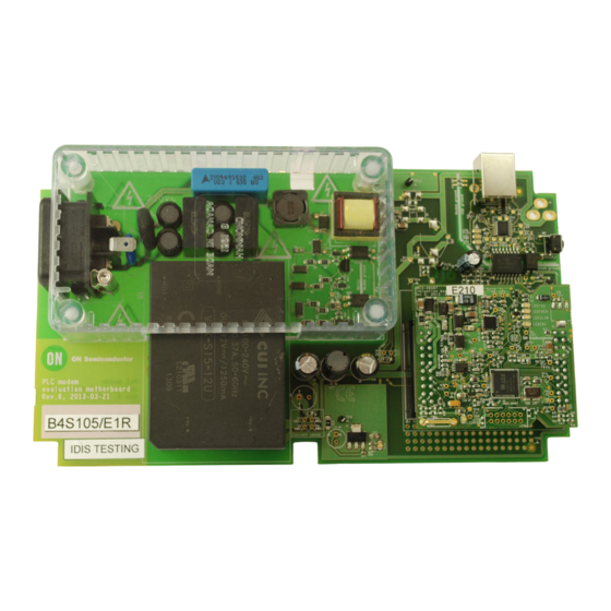
Page 2: Evaluation Boards
If damage is suspected, stop using the evaluation kit. The evaluation circuit is split up in a motherboard and Contact ON Semiconductor to have it re-tested and a daughterboard (Figure 1). Refer to [11, 14, 15] for the full repaired. - Page 3 If you would like to evaluate one 220 nF + 22 mH and 150 nF + 10 mH of the other transformers, contact your ON Semiconductor (Dashed, Left resp. Right) sales representative before ordering an evaluation kit.
- Page 4 To stop the transmission provided it supports the standard commands and it is IO3 is set high by the ON Semiconductor ON−PL110 addressed with a three bytes address. In practice, this will embedded software stack. This feature is not used by the IEC...
- Page 5 EVBUM2290/D (Daughterboard) OutA Memory Transmit Filter Line Driver Receive Filter Motherboard Modem Transformer Communication Figure 4. Daughterboard System-Level View Filters The “G” variant is optimized for the carrier frequencies of Daughterboards are available for the NCN49597 and the KNX PL110 standard, 105 and 115 kHz.
- Page 6 EVBUM2290/D “E” are commonly used with the IEC firmware for The transmit filter is always a low-pass filter , but the automatic meter reading, while ON−PL110 firmware users order depends on the variant. Variants requiring three poles typically use “G” and “J”. However, it bears repeating that...
- Page 7 EVBUM2290/D Using the Daughterboards The IEC or ON−PL110 firmware toggles IO0 at a faster The various test points on the daughterboard are marked rate. After it has been loaded the toggle frequency is about with diagonal crosses. The most important test points are 1 Hz.
- Page 8 EVBUM2290/D Driver Installation User Terminal Computer The serial port is encapsulated over USB as a virtual Commands communications port (VCP) by a converter chip. On Windows operating systems, specific drivers must be Terminal installed before this converter is recognized by the computer.
- Page 9 Terminal for PL110 → ON Semiconductor PLC Terminal PL110; The exact version is important, so make sure to use the Gtk# or Programs → ON Semiconductor PLC Terminal for IEC − installer supplied with the terminal installation program. Linky (HDLC API) → ON Semiconductor Terminal IEC − Linky Subsequently, the PC software installer can be run;...
- Page 10 EVBUM2290/D We will use the ports command that lists the available and First sets the MIB parameter MIB_R_FS1 to the not available serial ports in the system. The easiest way to hexadecimal value 159B; the second command will query find the connected serial port is to issue the command ports, the current value and should return the same 159B.
- Page 11 EVBUM2290/D By default, the ON−PL110 firmware looks for a mains For a graphical representation, use the spy window zero-crossing and synchronizes transmission with the (section “Advanced Terminal Features”). The separate “spy mains. If synchronization to the mains zero crossing is not window”...
- Page 12 EVBUM2290/D Note that by its nature, reception in PHY mode does not script cfg/slave.txt filter frames based on destination address; thus, all frames It is possible, and often convenient, to create customized will be reported by any modem that receives them.
- Page 13 Access to Different Network Layers Advanced Terminal Features • The IEC firmware from ON Semiconductor implements The log <level> command alters the amount of logging the three lowest layer defined by the IEC 61334 standard information shown. Use log −1 to disable all output; use (refer to [6, 7]): the physical (PHY), Media Access Control log 3 to shown as much logging as possible.
-
Page 14: Troubleshooting
EVBUM2290/D Attainable Communication Quality communication can be difficult due to the long electrical The practical communication range strongly depends on distance. Crosstalk with signals from modem C might also the network. It is mainly influenced by the attenuation influence the communication. - Page 15 EVBUM2290/D Is the Motherboard Receiving Serial Data? Is the Line Driver Overloaded? Two green LEDs on the motherboard light up when the If the transmit LED lights up but communication over the USB-to-serial converter is receiving and transmitting data. power line is still not possible, observe the red TSD (thermal...
- Page 16 EVBUM2290/D Figure 21. Oscilloscope Traces of the Line Driver Figure 23. Modem Output (Bottom Trace) and Line Output: Good (Top) and Undersampled Driver Output (Top Trace) during Thermal Overload Under normal conditions the line driver output is a close (though amplified) copy of the modem output (Figure 22...
- Page 17 EVBUM2290/D from transmitter to receiver. Also, do not connect other consumers to the distribution strip − this lowers the local noise and interference level. When it has been verified the transmitted is generating a strong signal the PL test point (section “Is the Line Driver Overloaded?”), observe the same test point on the receiver...
- Page 18 EVBUM2290/D Troubleshooting Performance version Displays the version of the PLC Terminal Sometimes the communication over the power line application. between two evaluation kits is functional but low-quality, oids Display all MIB object Ids. i.e. the receiving modem receives some but not all frames.
- Page 19 EVBUM2290/D • cdir [path to folder] Set current working directory for the bit. Bus idle delay, measured in bit times, before the terminal. The working directory is used as a base path when frame is sent on the power line by the PHY layer opening files specified with a relative path.
- Page 20 EVBUM2290/D txdelay [msec] Set the pause time between transmit requests available when the MAC layer of the modem is accessible; with commands txphy, txmac and txmacm. this is achieved by setting OID 6100 (TOPLAYER) to 1. • • msec. The pause time in milliseconds num.
- Page 21 EVBUM2290/D APPENDIX Evaluation Kit Design The copper design of the revision 6 motherboard and the Figures 27 and 28 . The bottom copper is shown mirrored, revision 3 NCN49597 daughterboard are shown in i.e. as if seen through the board.
- Page 22 EVBUM2290/D REFERENCES [1] CUI inc. VSK 15 W − AC−DC power supply, [13] ON Semiconductor. Getting started with the January 2013. Online at http://www.cui.com/ AMIS−49587 evaluation board (user manual product/resource/vsk-s15-series.pdf, accessed AMIS49587GEVB), July 2013. Online at 2013−12−19. http://www.onsemi.com/pub_link/Collateral/ [2] Électricité réseau distribution France, ERDF. Linky EVBUM2201−D.PDF.
- Page 23 onsemi, , and other names, marks, and brands are registered and/or common law trademarks of Semiconductor Components Industries, LLC dba “onsemi” or its affiliates and/or subsidiaries in the United States and/or other countries. onsemi owns the rights to a number of patents, trademarks, copyrights, trade secrets, and other intellectual property. A listing of onsemi’s product/patent coverage may be accessed at www.onsemi.com/site/pdf/Patent−Marking.pdf.
Need help?
Do you have a question about the EVBUM2290/D and is the answer not in the manual?
Questions and answers