Renesas RX200 Series User Manual
Evaluation kit for microcontroller
Hide thumbs
Also See for RX200 Series:
- User manual ,
- Quick start manual (23 pages) ,
- User manual (28 pages)
Table of Contents
Advertisement
Quick Links
RX261 Group
Evaluation Kit for RX261 Microcontroller Group
Renesas RX Family
RX200 Series
All information contained in these materials, including products and product specifications, represents
information on the product at the time of publication and is subject to change by Renesas Electronics
Corp. without notice. Please review the latest information published by Renesas Electronics Corp.
through various means, including the Renesas Electronics Corp. website (http://www.renesas.com).
www.renesas.com
EK-RX261 v1
User's Manual
Rev.1.00 Jul 2024
Advertisement
Table of Contents

Subscribe to Our Youtube Channel
Related Manuals for Renesas RX200 Series


Summary of Contents for Renesas RX200 Series
- Page 1 All information contained in these materials, including products and product specifications, represents information on the product at the time of publication and is subject to change by Renesas Electronics Corp. without notice. Please review the latest information published by Renesas Electronics Corp.
-
Page 2: Corporate Headquarters
Renesas Electronics disclaims any and all liability for any damages or losses incurred by you or any third parties arising from the use of any Renesas Electronics product that is inconsistent with any Renesas Electronics data sheet, user’s manual or other Renesas Electronics document. - Page 3 Unit Products The following usage notes are applicable to all Microprocessing unit and Microcontroller unit products from Renesas. For detailed usage notes on the products covered by this document, refer to the relevant sections of the document as well as any technical updates that have been issued for the products.
-
Page 4: Proprietary Notice
Renesas or its affiliates shall in no event be liable for any loss of profit, loss of data, loss of contract, loss of business, damage to reputation or goodwill, any economic loss, any reprogramming or recall costs (whether the foregoing losses are direct or indirect) nor shall Renesas or its affiliates be liable for any other direct or indirect special, incidental or consequential damages arising out of or in relation to the use of this EK-RX261, even if Renesas or its affiliates have been advised of the possibility of such damages. -
Page 5: Table Of Contents
User’s Manual Renesas RX Family EK-RX261 v1 User’s Manual Contents List of Abbreviations and Acronyms ....................5 Kit Overview ..........................6 Assumptions and Advisory Notes ......................9 Kit Contents ........................... 10 Ordering Information ......................10 Hardware Architecture and Default Configuration ..............11 Kit Architecture ............................ - Page 6 Renesas RX Family EK-RX261 v1 – User's Manual Miscellaneous ............................39 5.5.1 LED ..............................39 5.5.2 User and Reset Switches ........................40 Special Feature Access Area ....................41 CAN FD (Controller Area Network with Flexible Data Rate) ..............41 Touch Interface ............................42 MCU Native Pin Access Area ....................
- Page 7 Renesas RX Family EK-RX261 v1 – User's Manual Figure 17. Pmod 2 connector ........................30 Figure 18. Pmod 2 Pin header jumpers (top side) ..................31 Figure 19. Pmod 2 Copper jumpers (bottom side) ..................31 Figure 20. Arduino Uno Connectors (J7, J8, J9 and J10) ................33 Figure 21.
- Page 8 Renesas RX Family EK-RX261 v1 – User's Manual Table 18. FT234XD-T and RX MCU Connection ..................36 Table 19. USB Full Speed Connector ......................38 Table 20. USB Full Speed Pin Header Jumper Configuration ..............38 Table 21. USB FS Power Supply IC ......................38 Table 22.
-
Page 9: List Of Abbreviations And Acronyms
Renesas RX Family EK-RX261 v1 – User's Manual List of Abbreviations and Acronyms Table 1. List of Abbreviations and Acronyms Analog to Digital Converter Bill of Materials Bits Per Second Controller Area Network CAN FD CAN with Flexible Data Rate... -
Page 10: Kit Overview
Renesas RX Family EK-RX261 v1 – User's Manual 1. Kit Overview The EK-RX261 v1, an Evaluation Kit for RX261 MCU Group, enables users to seamlessly evaluate the features of the RX261 MCU group and develop embedded systems applications using Firmware Integration Technology (FIT) and e studio IDE. -
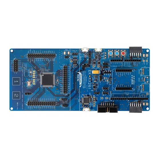
Page 11: Figure 1. Ek-Rx261 V1 Top Side
Renesas RX Family EK-RX261 v1 – User's Manual Grove and Qwiic Connectors mikroBus Connector Arduino Uno connectors Arduino Uno connectors (ANALOG and POWER) (DIGITAL) +5V IN and GND +3.3V and GND Test Points Test Points PMOD 2 Connector PMOD 1 Connector... -
Page 12: Figure 2. Ek-Rx261 V1 Bottom Side
Renesas RX Family EK-RX261 v1 – User's Manual I2C (RIICa) Pull-up Grove Configuration Configuration Copper Jumper Copper Jumpers Arduino (Power) I2C Pull-up Configuration Configuration Copper Jumpers Copper Jumper Pmod 1 Configuration Copper Jumpers Pmod 2 Configuration Copper Jumpers Arduino (Reset) -
Page 13: Assumptions And Advisory Notes
Renesas RX Family EK-RX261 v1 – User's Manual 1.1 Assumptions and Advisory Notes 1. It is assumed that the user has basic understanding of microcontrollers and embedded systems hardware. 2. It is recommended that the user refers to the EK-RX261 Quick Start Guide to get acquainted with the kit and the Quick Start example project that EK-RX261 v1 comes pre-programmed with. -
Page 14: Kit Contents
Renesas RX Family EK-RX261 v1 – User's Manual 2. Kit Contents The following components are included in the kit: EK-RX261 x 1 Micro USB function cable (type-A male to micro-B male) x 1 Micro USB host cable (type-A female to micro-B male) x 1 Ferrite core x 1 Figure 3. -
Page 15: Hardware Architecture And Default Configuration
Renesas RX Family EK-RX261 v1 – User's Manual 4. Hardware Architecture and Default Configuration 4.1 Kit Architecture The EK-RX261 v1 is designed with three areas to help shorten the learning curve of the users and maximize the design and knowledge reuse among similar kits. The contents of these three areas are conceptually standardized among similar kits. -
Page 16: Figure 4. Ek-Rx261 V1 Area Definitions
Renesas RX Family EK-RX261 v1 – User's Manual System Control and Ecosystem Access Area Special Feature Access Area MCU Native Pin Access Area Figure 4. EK-RX261 v1 Area Definitions R20UT5351EG0100 Rev.1.00 Page 12 of 49 Jul.31.24... -
Page 17: System Block Diagram
Renesas RX Family EK-RX261 v1 – User's Manual 4.2 System Block Diagram External debugger connector Debug I/F USB Micro B E2 OB circuit connector Power 3.3V Linear Regulator Debug LED Power LED Reset Switch Reset Main clock 8MHz crystal oscillator oscillator 32.768kHz crystal... -
Page 18: Component Placement Location And Dimension
Renesas RX Family EK-RX261 v1 – User's Manual 4.3 Component Placement Location and Dimension Reference number for components on the EK-RX261 v1 is shown below. TP11 TP12 TP13 TP14 R48 C55 LED5 LED4 FIL1 TP10 Figure 6. Reference number for components on the EK-RX261 v1 (top side) R20UT5351EG0100 Rev.1.00... -
Page 19: Figure 7. Reference Number For Components On The Ek-Rx261 V1 (Bottom Side)
Renesas RX Family EK-RX261 v1 – User's Manual Figure 7. Reference number for components on the EK-RX261 v1 (bottom side) R20UT5351EG0100 Rev.1.00 Page 15 of 49 Jul.31.24... -
Page 20: Figure 8. Dimension Of The Ek-Rx261 V1
Renesas RX Family EK-RX261 v1 – User's Manual Dimension of the EK-RX261 v1 is shown below. 64.13mm 28.57mm Diameter 15.87mm 3.3mm 22.86mm J3: 2 x 14 pin J1: 2 x 6 pin 8.25mm 23.49mm 64.13mm 71.75mm 80.00mm Figure 8. Dimension of the EK-RX261 v1 R20UT5351EG0100 Rev.1.00... -
Page 21: Jumper Settings
Renesas RX Family EK-RX261 v1 – User's Manual 4.4 Jumper Settings Two types of jumpers are provided on the EK-RX261 v1. 1. Copper jumpers (trace-cut type and solder bridge type) 2. Traditional pin header jumpers The following sections describe each type and their default configuration. -
Page 22: Table 3. Default Jumper Settings
Renesas RX Family EK-RX261 v1 – User's Manual Table 3. Default Jumper Settings Location Circuit Group Default Function RX261 MCU Closed RX MCU Current Measurement Power Supply Jumper on pins 1-2 Connect Board_VCC to 3.3V USB FS Open USB FS operating mode. Function (Self-power) mode is configured at shipping. - Page 23 Renesas RX Family EK-RX261 v1 – User's Manual Location Circuit Group Default Function Arduino Uno Closed Connect P12(SCL0) and P13(SDA0) to Board_VCC(Pull-up) Arduino Uno Open Connect 5.0V to J7-Pin5(5V) Arduino Uno Closed Connect 3.3V to J7-Pin4(3.3V) Arduino Uno Closed Connect Board_VCC to J7-Pin2(IOREF)
-
Page 24: System Control And Ecosystem Access Area
Renesas RX Family EK-RX261 v1 – User's Manual 5. System Control and Ecosystem Access Area The following figure shows the System Control and Ecosystem Access area on the EK-RX261 v1. Subsequent sections detail the features and functionality provided in the area. -
Page 25: Usb Debug1
Renesas RX Family EK-RX261 v1 – User's Manual 3.3V Voltage Main System 5V Measurement : Power (5.0 V) TP3 and TP4 5V to 3.3V USB DEBUG1 Linear RX MCU Current (J26) Regulator Measurement RX MCU TP1 & TP2 USB FULL SPEED... -
Page 26: Debug
Renesas RX Family EK-RX261 v1 – User's Manual 5.2 Debug The EK-RX261 v1 supports the following two debug modes. Table 4. Debug Modes Debug Modes Debug MCU Target MCU Debugging Connector Used (one that (one that is being Interface/Protocol connects to the... -
Page 27: Figure 12. Ek-Rx261 V1 Debug Interface
Renesas RX Family EK-RX261 v1 – User's Manual 14-pin male box header for external debugger USB Connector (USB DEBUG1) Figure 12. EK-RX261 v1 Debug Interface R20UT5351EG0100 Rev.1.00 Page 23 of 49 Jul.31.24... -
Page 28: Debug On-Board
Renesas RX Family EK-RX261 v1 – User's Manual 5.2.1 Debug On-Board The debug on-board functionality is provided using E2 OB circuit on the EK-RX261 v1. USB DEBUG1 connector (J26) connects the E2 OB circuit to a host PC, allowing re-programming and debugging of the target RX MCU firmware. -
Page 29: Debug In
MD / FINED MD_FINED J27-8 Board_VCC J27-9 N.C. N.C. PC7 (UB) J27-10 J27-11 N.C. J27-12 J27-13 RES# RES# J27-14 Note 1: The signals are available as TXD and RXD at using Renesas Flash Programmer. R20UT5351EG0100 Rev.1.00 Page 25 of 49 Jul.31.24... -
Page 30: Ecosystem
Renesas RX Family EK-RX261 v1 – User's Manual 5.3 Ecosystem The System Control and Ecosystem area provides users the means to connect third party add-on modules compatible with five most popular ecosystems using the following connectors: 1. Two Seeed Grove... -
Page 31: Sparkfun ® Qwiic ® Connector
Renesas RX Family EK-RX261 v1 – User's Manual Table 11. Grove 2 Connector Grove 2 Connector EK-RX261 v1 Configuration Description Signal Closed Open J12-1 SCL / AN PB6 (RXD009 / SMISO009 / SSCL009) E29, E46 P46 (AN006) J12-2 SDA / AN... -
Page 32: Digilent Pmod™ Connectors
Renesas RX Family EK-RX261 v1 – User's Manual 5.3.3 Digilent Pmod™ Connectors 5.3.3.1 Pmod 1 A 12-pin Pmod Type-2A (expanded SPI), Type-3A (expanded UART) and Type-6A (expanded I connector is provided at connector J28 labelled PMOD1. At Type-2A, the RX MCU acts as the SPI master, and the connected module acts as an SPI slave device. -
Page 33: Figure 15. Pmod 1 Pin Header Jumpers (Top Side)
Renesas RX Family EK-RX261 v1 – User's Manual Pmod 1 Type-6A connection The option for Type-6A (I C) can be configured at Pmod 1 and supports 3.3 V / 5 V devices. To configure the EK-RX261 v1 to use the I C devices with 3.3 V / 5 V operation, configure the pin header jumpers and the... -
Page 34: Figure 17. Pmod 2 Connector
Renesas RX Family EK-RX261 v1 – User's Manual 5.3.3.2 Pmod 2 A 12-pin Pmod Type-2A (expanded SPI), Type-3A (expanded UART) and Type-6A (expanded I connector is provided at connector J29 labelled PMOD2. At Type-2A, the RX MCU acts as the SPI master, and the connected module acts as an SPI slave device. -
Page 35: Figure 18. Pmod 2 Pin Header Jumpers (Top Side)
Renesas RX Family EK-RX261 v1 – User's Manual Pmod 2 Type-6A connection The option for Type-6A (I C) can be configured at Pmod 2 and supports 3.3 V / 5 V devices. To configure the EK-RX261 v1 to use the I C devices with 3.3 V / 5 V operation, configure the pin header jumpers and the... -
Page 36: Arduino ® Connector
Renesas RX Family EK-RX261 v1 – User's Manual 5.3.4 Arduino ® Connector Near the center of the System Control and Ecosystem Access area is an Arduino Uno R3 compatible connector interface. Table 15. Arduino Uno Connections Arduino Compatible Connector EK-RX261 v1... -
Page 37: Figure 20. Arduino Uno Connectors (J7, J8, J9 And J10)
Renesas RX Family EK-RX261 v1 – User's Manual J7-Pin1 Arduino Uno (J7) (POWER) J8-Pin1 Arduino Uno (J8 & J10) (DIGITAL) J9-Pin1 Arduino Uno (J9) (ANALOG) J10-Pin1 Figure 20. Arduino Uno Connectors (J7, J8, J9 and J10) Figure 21. Arduino Uno Copper jumpers (bottom side) -
Page 38: Mikroelektronika Mikrobus™ Connector
Renesas RX Family EK-RX261 v1 – User's Manual 5.3.5 MikroElektronika mikroBUS™ Connector In the center of the System Control and Ecosystem Access area is a mikroBUS compatible connector interface. This interface is compliant with mikroBUS Standard Specifications revision 2.00. Table 16. mikroBUS Connections... -
Page 39: Figure 22. Mikrobus Connectors
Renesas RX Family EK-RX261 v1 – User's Manual Figure 22. mikroBUS Connectors mikroBUS CLICK BOARD Considerations The EK-RX261 v1 can supply 5 V power to J15-Pin7 of mikroBUS CLICK BOARD by soldering copper jumper E32, however, some of the RX MCU pins which are connected to mikroBUS CLICK BOARD are not 5 V tolerant. -
Page 40: Connectivity
Renesas RX Family EK-RX261 v1 – User's Manual 5.4 Connectivity 5.4.1 USB to Serial The USB Micro-B connecter (J16) connects the RX MCU SCI interface to an external USB interface through FTDI FT234XD-T (U3) with maximum baud rate of 3Mbps. The RX MCU SCI can be configured either SCI6 (default configuration) or SCI1. -
Page 41: Usb Full Speed
Renesas RX Family EK-RX261 v1 – User's Manual Figure 24. USB to Serial Copper jumpers (bottom side) The user must install FTDI Virtual COM Port (VCP) driver from FTDI’s web site to use FT234XD-T. https://ftdichip.com/ 5.4.2 USB Full Speed The USB Micro-AB connecter (J20) connects the RX MCU USB Full Speed interface to an external USB interface, allowing communications for testing and use of the RX MCU firmware. -
Page 42: Figure 25. Usb Full Speed Connector
Renesas RX Family EK-RX261 v1 – User's Manual Table 19. USB Full Speed Connector USB Full Speed Connector EK-RX261 v1 Description Signal J20-1 +5 VDC +5V_USBFS (Function Mode) +5V_H_USBFS (Host Mode) J20-2 Data- USB0_DM J20-3 Data+ USB0_DP J20-4 USB ID, jack internal switch, cable inserted N.C. -
Page 43: Miscellaneous
Renesas RX Family EK-RX261 v1 – User's Manual 5.5 Miscellaneous 5.5.1 LED 5 LEDs are provided on the EK-RX261 v1. Behavior of the LEDs on the EK-RX261 v1 is described in the following table. User LEDs are active high on the RX MCU ports. -
Page 44: User And Reset Switches
Renesas RX Family EK-RX261 v1 – User's Manual 5.5.2 User and Reset Switches Three miniature, momentary, mechanical push-button type SMT switches are mounted on the EK-RX261 v1. Pressing the Reset switch (S3) generates a reset signal to reset the RX MCU. -
Page 45: Special Feature Access Area
Renesas RX Family EK-RX261 v1 – User's Manual 6. Special Feature Access Area The Special Feature Access area provides features specific to the RX MCU group such as CAN FD and Touch interface. Figure 32. Special Feature Access Area 6.1 CAN FD (Controller Area Network with Flexible Data Rate) A CAN FD transceiver IC is provided on the EK-RX261 v1. -
Page 46: Touch Interface
Renesas RX Family EK-RX261 v1 – User's Manual 6.2 Touch Interface The RX MCU incorporates Capacitive Touch Sensing Unit (CTSU2SL), and the CTSU is connected to 2 touch buttons on the EK-RX261 v1. Table 26. Touch Interface EK-RX261 v1 RX MCU... -
Page 47: Mcu Native Pin Access Area
Renesas RX Family EK-RX261 v1 – User's Manual 7. MCU Native Pin Access Area Figure 35. Native Pin Access Area 7.1 Breakout Pin Headers The EK-RX261 v1 pin headers, J1, J2, J3 and J4, provide access to RX MCU signals. Each header pin is labeled with the power or port connected to that pin. -
Page 48: Mcu Operating Mode
Renesas RX Family EK-RX261 v1 – User's Manual Figure 36. RX MCU Current Measurement Circuit Figure 37. Pin Header Jumper J5 7.3 MCU Operating Mode MCU operating mode is configured by pin header jumpers (J22, J23, J24 and J25). Table 27. MCU Operating Mode Configuration... -
Page 49: Recommended Components
Renesas RX Family EK-RX261 v1 – User's Manual 8. Recommended Components Table 28 lists recommended part numbers for the components that can be fitted as required. Table 28. Recommended Components Designator(s) Description Manufacturer Part Number Feedback resistor of The resistance must be adjusted by crystal oscillator Y1 users. -
Page 50: Certifications
Renesas RX Family EK-RX261 v1 – User's Manual 9. Certifications The EK-RX261 v1 meets the following certifications/standards. See page 4 of this user’s manual for the disclaimer and precautions. 9.1 EMC/EMI Standards FCC Notice (Class A) • This device complies with part 15 of the FCC Rules. Operation is subject to the following two conditions: (1) This device may not cause harmful interference, and (2) this device must accept any interference received, including interference that may cause undesired operation. -
Page 51: Material Selection, Waste, Recycling And Disposal Standards
WEEE must be treated, recycled and disposed of in an environmentally sound manner. Renesas Electronics Europe GmbH can take back end of life equipment. Register for this service at; https://www.renesas.com/eu/en/support/regional-customer-support/weee 9.3 Safety Standards... -
Page 52: Design And Manufacturing Information
Renesas RX Family EK-RX261 v1 – User's Manual 10. Design and Manufacturing Information The design and manufacturing information for the EK-RX261 v1 is available in the “EK-RX261 v1 Design Package” available on renesas.com/rx/ek-rx261. Design package file name: ek-rx261-v1-designpackage.zip • Design package contents •... -
Page 53: Revision History
Renesas RX Family EK-RX261 v1 – User's Manual Revision History Rev. Date Description Page Summary 1.00 Jul.31.24 — Initial release R20UT5351EG0100 Rev.1.00 Page 49 of 49 Jul.31.24... - Page 54 D010816-24-V0300 ● 有害物質の含有表 Table of Hazardous Substance 部品名称 有害物質 Part Name Hazardous Substance 鉛 水銀 カドミウム 六価クロム ポリ臭化ビフェニル ポリ臭化ジフェニルエーテル Lead Mercury Cadmium Hexavalent Polybrominated Polybrominated (Pb) (Hg) (Cd) Chromium biphenyls diphenyl ethers (Cr(VI)) (PBB) (PBDE) 筐体 Case ボード Board ケーブル Cable ソケット...
- Page 55 D010816-24-V0300 ● 有害物质含有情况表 Table of Hazardous Substance 部件名称 有害物质 Part Name Hazardous Substance 铅 汞 镉 六价铬 多溴联苯 多溴二苯醚 Lead Mercury Cadmium Hexavalent Polybrominated Polybrominated (Pb) (Hg) (Cd) Chromium biphenyls diphenyl ethers (Cr(VI)) (PBB) (PBDE) 外壳 Case 电路板 Board 连接线 Cable 插座...
- Page 56 EK-RX261 v1 – User’s Manual Publication Date: Jul.31.24 Rev.1.00 Published by: Renesas Electronics Corporation...
- Page 57 EK-RX261 v1 – User’s Manual R20UT5351EG0100...
Need help?
Do you have a question about the RX200 Series and is the answer not in the manual?
Questions and answers