Table of Contents
Advertisement
Quick Links
Features
• First USB Host/Slave controller for embedded systems in
the market with a standard microprocessor bus interface
• Supports both full speed (12 Mbps) and low speed (1.5
Mbps) USB transfer in both master and slave modes
• Conforms to USB Specification 1.1 for full- and low speed
• Operates as a single USB host or slave under software
control
• Automatic detection of either low- or full speed devices
• 8-bit bidirectional data, port I/O (DMA supported in slave
mode)
• On-chip SIE and USB transceivers
• On-chip single root HUB support
• 256-byte internal SRAM buffer
• Ping-pong buffers for improved performance
• Operates from 12 or 48 MHz crystal or oscillator (built-in
DPLL)
• 5V-tolerant interface
• Suspend/resume, wake up, and low-power modes are
supported
• Auto-generation of SOF and CRC5/16
• Auto-address increment mode, saves memory
READ/WRITE cycles
• Development kit including source code drivers is available
• 3.3V power source, 0.35 micron CMOS technology
• Available in both a 28-pin PLCC package and a 48-pin
TQFP package
Block Diagram
D
USB
+
Root HUB
D-
XCVRS
Cypress Semiconductor Corporation
Document 38-08008 Rev. *D
SL811HS Embedded USB Host/Slave Controller
Master/Slave
Controller
SERIAL
INTERFACE
ENGINE
CLOCK
GENERATOR
X1
X2
•
198 Champion Court
Introduction
The SL811HS is an Embedded USB Host/Slave Controller
capable of communicating in either full speed or low speed.
The SL811HS interfaces to devices such as microprocessors,
microcontrollers, DSPs, or directly to a variety of buses such
as ISA, PCMCIA, and others. The SL811HS USB Host
Controller conforms to USB Specification 1.1.
The SL811HS incorporates USB Serial Interface functionality
along with internal full or low speed transceivers. The
SL811HS supports and operates in USB full speed mode at 12
Mbps, or in low speed mode at 1.5 Mbps. When in host mode,
the SL811HS is the master and controls the USB bus and the
devices that are connected to it. In peripheral mode, otherwise
known as a slave device, the SL811HS operates as a variety
of full- or low speed devices.
The SL811HS data port and microprocessor interface provide
an 8-bit data path I/O or DMA bidirectional, with interrupt
support to allow easy interface to standard microprocessors or
microcontrollers such as Motorola or Intel CPUs and many
others. The SL811HS has 256-bytes of internal RAM which is
used for control registers and data buffer.
The available package types offered are a 28-pin PLCC
(SL811HS) and the lead-free packages are a 28-pin
(SL811HS-JCT) and a 48-pin (SL811HST-AXC) package. All
packages operate at 3.3 VDC. The I/O interface logic is
5V-tolerant.
INTERRUPT
CONTROLLER
256 Byte RAM
BUFFERS
&
CONTROL
REGISTERS
PROCESSOR
INTERFACE
,
•
San Jose
CA 95134-1709
SL811HS
INTR
nDRQ
DMA
Interface
nDACK
nW R
nRD
nCS
nRST
D0-7
•
408-943-2600
Revised February 2, 2007
Advertisement
Table of Contents

Subscribe to Our Youtube Channel
Related Manuals for Cypress Semiconductor SL811HS


Summary of Contents for Cypress Semiconductor SL811HS
-
Page 1: Block Diagram
SL811HS supports and operates in USB full speed mode at 12 Mbps, or in low speed mode at 1.5 Mbps. When in host mode, the SL811HS is the master and controls the USB bus and the devices that are connected to it. In peripheral mode, otherwise known as a slave device, the SL811HS operates as a variety of full- or low speed devices. - Page 2 SL811HS provides a DMA in- terface. This interface supports DMA READ or WRITE trans- fers to the SL811HS internal RAM buffer, it is done through the microprocessor data bus via two control lines (nDRQ - Data Request and nDACK - Data Acknowledge), along with the nWR line and controls the data flow into the SL811HS.
- Page 3 12 MHz , series, 20-pF load 22 pF Note 1. CM (Clock Multiply) pin of the SL811HS must be tied to GND when 48 MHz crystal circuit or 48 MHz clock source is used. Document 38-08008 Rev. *D Typical Crystal Requirements The following are examples of ‘typical requirements.’...
- Page 4 “Bus Interface Timing Requirements” on page provide control and status information for USB transactions. Any write to control register 0FH enables the SL811HS full features bit. This is an internal bit of the SL811HS that enables additional features. Table 1 shows the memory map and register mapping of the SL811HS in master/host mode.
- Page 5 HBADD5 The USB-A/B Base Address is a pointer to the SL811HS memory buffer location for USB reads and writes. When transferring data OUT (Host to Device), the USB-A and USB-B Host Base Address registers can be set up before setting ARM on the USB-A or USB-B Host Control register.
-
Page 6: Setup
1023 bytes since the SL811HS only has an 8-bit length; the maximum packet size for the ISO mode using the SL811HS is 255 – 16 bytes (register space). When the Host Base length register is set to zero, a Zero-Length packet is transmitted. -
Page 7: Bit 5
The next set of registers are the Control registers and control more of the operation of the chip instead of USB packet type of transfers. Table 10 is a summary of the control registers. Table 10. SL811HS Control Registers Summary Register Name SL811H Control Register 1 Interrupt Enable Register... -
Page 8: Bit 7
There are two cases when communicating with a low speed device. When a low speed device is connected directly to the SL811HS, bit 5 of Register 05h is set to ’1’ and bit 6 of register 0Fh, Polarity Swap, is set to ’1’ in order to change the polarity of D+ and D–. -
Page 9: Bit 6
Interrupt Enable Register [Address = 06h]. The SL811HS provides an Interrupt Request Output, which is activated for a number of conditions. The Interrupt Enable register allows the user to select conditions that result in an interrupt that is issued to an external CPU through the INTRQ pin. A separate Interrupt Status register reflects the reason for the interrupt. - Page 10 Device Insert/Remove Detection. Bit 5 is provided to support USB cable insertion/removal for the SL811HS in host mode. This bit is set when a transition from SE0 to IDLE (device inserted) or from IDLE to SE0 (device removed) occurs on the bus.
- Page 11 SOF High Counter Register Note Any write to Control register 0Fh enables the SL811HS full features bit. This is an internal bit of the SL811HS that enables additional features. The USB-B register set is used when SL811HS full feature bit is enabled.
- Page 12 Reserved Memory Buffer 40h – FFh When in slave mode, the registers in the SL811HS are divided into two major groups. The first group contains Endpoint reg- isters that manage USB control transactions and data flow. The second group contains the USB Registers that provide the control and status information for all other operations.
- Page 13 Endpoint Base Length [Address a = (EP# * 10h)+2, b = (EP# * 10h)+A]. The Endpoint Base Length is the maximum packet size for IN/OUT transfers with the host. Essentially, this designates the largest packet size that is received by the SL811HS with an OUT transfer, or it designates the size of the data packet sent to the host for IN transfers.
- Page 14 Endpoint Packet Status register and is considered a serious error. EPxCNT4 EPxCNT3 unique identifier, which is the Endpoint Number. For more details about USB endpoints, refer to the USB Specification 1.1, Section 5.3.1. SL811HS Time-out Error EPxCNT2 EPxCNT1 EPxCNT0 Address (in Hex)
- Page 15 J-K0 These two bits are set to zero on power up, see DMA Dir DMA Transfer Direction. Set equal to ‘1’ for DMA READ cycles from SL811HS. Set equal to ‘0’ for DMA WRITE cycles. DMA Enable Enable DMA operation when equal to ‘1’. Disable = ‘0’. DMA is initiated when DMA Count High is written.
- Page 16 Endpoint 1 Done Interrupt. Endpoint 0 Done Endpoint 0 Done Interrupt. Document 38-08008 Rev. *D SL811HS initiated the interrupt (see the description in section Status Register, Address corresponding interrupt is enabled. Setting a bit in the Interrupt Enable register does not effect the Interrupt Status register’s value;...
- Page 17 Function only register ferred between a peripheral to the SL811HS. The count may sometimes require up to 16 bits, therefore the count is repre- sented in two registers: Total Count Low and Total Count High. EP3 is only supported with DMA operation.
-
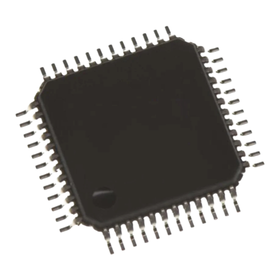
Page 18: Physical Connections
Physical Connections These parts are offered in both a 28-pin PLCC package and a 48-pin TQFP package. The 28-pin PLCC packages are the SL811HS and SL811HS-JCT. The 48-pin TQFP packages is the SL811HST-AXC. 28-Pin PLCC Physical Connections 28-Pin PLCC Pin Layout... - Page 19 Zener 3.9v, 1N52288CT- Package Markings (28-pin PLCC) Part Number YYWW-X.X XXXX YYWW = Date code XXXX = Product code X.X = Silicon revision number Document 38-08008 Rev. *D 2N2222 +3.3 V (VDD) Sample VDD Generator SL811HS Page 19 of 32...
- Page 20 Pin and Signal Description for Pins 43 and 44 in Host Mode. 48-Pin TQFP Mechanical Dimensions Note 4. NC. Indicates No Connection. NC Pins must be left unconnected. Document 38-08008 Rev. *D nDACK* nDRQ* 48-Pin TQFP nRST Clk/X1 INTRQ SL811HS Page 20 of 32...
- Page 21 48/28-Pin USB Host Controller Pins Description The SL811HST-AXC is packaged in a 48-pin TQFP. The SL811HS and SL811HS-JCT packages are 28-pin PLCC’s. These devices require a 3.3 VDC power source. The 48-Pin TQFP requires an external 12 or 48 MHz crystal or clock.
- Page 22 DMA controller. nDRQ and nDACK form the handshake for DMA data transfers. In host mode, leave the pin unconnected. Read Strobe Input. An active LOW input used with nCS to read registers/data memory. No connection. No connection. No connection. SL811HS Page 22 of 32...
- Page 23 SL811HS Package Markings (48-Pin TQFP) Part Number YYW W -X.X XXXX YYWW = Date code XXXX = Product code X.X = Silicon revision number Document 38-08008 Rev. *D Page 23 of 32...
-
Page 24: Electrical Specifications
Electrical Specifications Absolute Maximum Ratings This section lists the absolute maximum ratings of the SL811HS. Stresses above those listed can cause permanent damage to the device. Exposure to maximum rated conditions for extended periods can affect device operation and reliability. - Page 25 16. All typical values are V = 3.3V and T 17. Z impedance values includes an external resistor of 24 Ohms ± 1% (SL811HS revision 1.2 requires external resistor values of 33 Ohms ±1%). USBX Document 38-08008 Rev. *D Description = 4 mA) = –4 mA)
- Page 26 Register or Memory Address twshld Min. 85 ns 0 ns 0 ns 85 ns 10 ns 85 ns 5 ns 85 ns 85 ns SL811HS twrhigh twdsu twdhld DATA Tcscs See Note. Typ. Max. Page 26 of 32...
- Page 27 Note nCS can be kept LOW during multiple Read cycles provided nRD is cycled. Rd Cycle Time for Auto Inc Mode Reads is 170 ns minimum. Document 38-08008 Rev. *D twahld trdp twdhld Register or Memory Address trcsu I/O Read Cycle from Register or Memory Buffer Description SL811HS twrrdl tracc trdhld DATA trshld Tcscs *Note Min. Typ. Max. 85 ns...
- Page 28 SL811 D M A W R IT E C Y C LE TIM IN G Description Min. 80 ns 5 ns 5 ns 65 ns 5 ns 60 ns 5 ns 5 ns 150 ns SL811HS tackrq D AT A tdw rp tdhld tackw rh Typ. Page 28 of 32 Max.
- Page 29 0 ns 5 ns 90 ns 5 ns 85 ns 0 ns 5 ns 150 ns treset tioact Reset Timing Description Min. 16 clocks 16 clocks SL811HS tdakrq D A T A tdhld Typ. Typ. Page 29 of 32 Max. Max.
-
Page 30: Ordering Information
Clock Period (48 MHz) Clock HIGH Time HIGH Clock LOW Time Clock Rise Time RISE Clock Fall Time FALL Clock Duty Cycle Ordering Information Part Number SL811HS SL811HS-JCT SL811HST-AXC Package Diagrams PIN #1 ID 0.450 0.485 0.458 0.495 Document 38-08008 Rev. *D tlow... - Page 31 48-Lead Thin Plastic Quad Flat Pack (7x7x1.4 mm) A48 Intel is a registered trademark of Intel Corporation. Torex is a trademark of Torex Semiconductors, Ltd. SL811HS is a trademark of Cypress Semiconductor Corporation. All product and company names mentioned in this document may be the trademarks of their respective holders.
- Page 32 Document History Page Document Title: SL811HS Embedded USB Host/Slave Controller Document Number: 38-08008 REV. ECN NO. Issue Date 110850 12/14/01 112687 03/22/02 381894 See ECN 464641 See ECN 749518 See ECN Document 38-08008 Rev. *D Orig. of Description of Change...
Need help?
Do you have a question about the SL811HS and is the answer not in the manual?
Questions and answers