
Related Manuals for SVS-Vistek GiGE CXP-12 SWIR Series


Summary of Contents for SVS-Vistek GiGE CXP-12 SWIR Series
- Page 1 Manual SWIR series fxo990MCX, fxo990MU3, fxo992MXGE, fxo993MXGE, fxo992MXGE-T, fxo993MXGE-T, fxo992MCX, fxo993MCX, fxo992MCX-T, fxo993MCX-T...
-
Page 2: Table Of Contents
Content General information Company information 1.1.1 Disclaimer 1.1.2 Copyright notice 1.1.3 Rules and regulations for Europe 1.1.4 Rules and regulations for USA and Canada Legal information 1.2.1 Rules and regulations for USA and Canada 1.2.2 Rules and regulations for Europe About this manual 1.3.1 Registered trademarks... - Page 3 Getting started Support Find camera specs Power supply 4.3.1 Power safety 4.3.2 Connect the camera 4.3.3 Using PoE (Power over Ethernet) 4.3.4 Using camera I/Os with PoCXP (Power over CXP) Camera status LED codes Feature description Basic features 5.1.1 Gain 5.1.2 Resolution 5.1.3...
- Page 4 5.3.7 Serial data interfaces 5.3.8 Trigger-edge sensitivity 5.3.9 Debouncing trigger signals 5.3.10 Prescale Annex Dimensions I/O driver circuit schematics Action commands Glossary List of figures Fig. 2-1: Illustration of 4I/O concept of switching LEDs Fig. 3-1: RJ45 socket connector Fig. 3-2: Data reduction with jumbo frames Fig.
- Page 5 Fig. 5-23: Several gamma curves comparable to a LUT Fig. 5-24: Several gamma curves comparable to a LUT Fig. 5-25: AOI on area sensor Fig. 5-26: Mode 0 - Free running with programmable exposure time Fig. 5-27: Mode 1: External Trigger with Pulse Width Exposure Control (overlap) Fig.
-
Page 7: General Information
No claims can be derived from the illus- trations in this manual. The product has been produced with care and has been thoroughly tested. In case of any complaint, contact your local SVS-VISTEK distributor. You will find a list of distributors in your area on www.svs-vistek.com 1.1.2... -
Page 8: Rules And Regulations For Europe
Customers, integ- rators and end users of SVS-VISTEK products might sell these products and agree to do so at their own risk, as SVS-VISTEK will not take any liability for any damage from improper use or sale. -
Page 9: Rules And Regulations For Europe
2011/65/EU Restriction of the use of certain hazardous substances in elec- trical and electronic equipment (RoHS) All products of SVS-Vistek GmbH comply with the recommendation of the European Union concerning RoHS rules. About this manual This manual contains helpful information to install and operate the described camera. -
Page 10: Registered Trademarks
1.3.1 Registered trademarks In this manual the following registered trademarks may be used: EoSens® GenICam® Microsoft® and Windows® Intel® Throughout the manual, these trademarks are not specifically marked as registered trademarks. This in no way implies that these trademarks can be used in another context without the trademark sign. -
Page 11: Warranty And Non-Warranty Clause
Doing so will void war- ranty. Our warranty does not protect against accidental damage, loss, or acts of nature. INFO SVS-Vistek GmbH cannot be held responsible for the loss of data. We recom- mend a backup plan. 1.3.4 Supplements For customers in Canada This apparatus complies with the Class A limits for radio noise emissions set out in Radio Interference Regulations. -
Page 12: Tips And Notes
SVS-Vistek GmbH for any damages resulting from such improper use or sale. Tips and notes This manual contains notes that help to avoid data loss or camera damage, and tips that provide information to improve handling the camera. They are marked... -
Page 13: The Fxo Camera Series
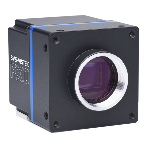
The FXO camera series The FXO is a camera series designed for high-end machine vision with a C- mount connection. Only Sony image sensors with excellent optical performance and high bandwidth are used in the FXO. Advanced electronic circuitry, an excel- lent temperature management and low power dissipation make the basis for optimal performance of even the most demanding image sensors. -
Page 14: Cxp-12 Features
4I/O adds light and functionality Fig. 2-1: Illustration of 4I/O concept of switching LEDs Your SVS-VISTEK camera is equipped with the innovative 4I/O-interface allow- ing full light control, replacing external strobe controllers. Each of the outputs can be individually configured and managed using pulse width modulation. With its high current output, the camera is able to drive LED lights directly without external light controller. -
Page 15: Lens Control
Lens control Various SVCam models are supporting adjustable lenses. Focus and iris of the lens can be controlled from within the camera GenICam tree. A special Y-cable might be required, contact sales@svs-vistek.com. The following variable lens types are supported: ... -
Page 16: Use Of Canon Lenses
Liquid lenses do have some advantages and disadvantages compared to glass optics: Advantages of liquid lenses Extremely robust to mechanical shock (best choice for fast moving robotics) and acceleration Fast focus (often significantly faster than 10 ms under common con- ditions) ... -
Page 17: Connectors
3.1.1 Automatic camera detection By default, SVS-VISTEK GigE Vision cameras are trying to acquire a valid network address via LLA or DHCP from the network. INFO Make sure to have valid network protocol with "Jumbo frames"... - Page 18 To change automatic address or to go back to automatic mode, configure the IP settings manually. You find the settings in the drop down menu TL Settings. Manual IP configuration allows to Assign a new IP address (make sure the new address is unique and valid in the current subnet) ...
-
Page 19: Gige Vision
For saving an persistent IP configuration (configuration will survive power off) check enable „Persistent IP address“. GigE Vision 3.2.1 Network (TCP/IP) Address Assignment By default, the camera does not have a persistent IP address. When forcing an IP address by using the PC internal network dialog, changes are only valid until the next restart of the Camera. -
Page 20: Fig. 3-2: Data Reduction With Jumbo Frames
upon each data packet sent. Jumbo frames increase the data size per Ethernet packet. Fig. 3-2: Data reduction with jumbo frames INFO Higher packet sizes require network cards that support jumbo packets. Lost packets In accordance with the PCT protocol, lost or corrupted packets will be resent. NOTICE Resends result in higher consumption of bandwidths and will lead to drop frames. -
Page 21: Xml Files
Fig. 3-3: Connecting multiple cameras on multi NICs Multiple cameras connected by a switch To connect multiple cameras by a switch, the switch must be managed. It might also be necessary to operate the cameras in an “inter packet delay” applying a smother image data stream. -
Page 22: 10 Gige Limitations And Issues
Special NICs support 100% connections without frame drops. 3.3.3 Recommended setup It is recommended to use a 10 GigE Ethernet card with grabber capabilities. All SVS-VISTEK certification setups are using this kind of cards. Contact sales@svs-vistek.com for details and more recommendations. -
Page 23: Hirose I/O Connector
The connectors are µBNC connectors. For cables, an impedance of 75 Ohm, RG187 is recommended. SVS-Vistek GmbH uses connectors according to JIIA standard. The CoaXPress standard supports camera control and power over CoaXPress (PoCXP). INFO It is recommended to use the frame grabber power supply over CoaXPress (PoCXP). -
Page 24: Getting Started
Put your support request to us via the support form: https://www.svs-vistek.- com/en/support/svs-support-request.php Fill the form with information about the camera model, the frame grabber model, and operating system. -
Page 25: Using Poe (Power Over Ethernet)
Using PoE (Power over Ethernet) Ethernet lines are able to provide the necessary power to operate Ethernet devices (Power over Ethernet). Some SVS-VISTEK GigE / 10GigE camera models are equipped with the capability to use power supply via the Ethernet lines (PoE). -
Page 26: Using Camera I/Os With Pocxp (Power Over Cxp)
4.3.4 Using camera I/Os with PoCXP (Power over CXP) Fig. 4-1: Connection diagram for PoCXP output The camera is grounded via the frame grabber card in the PC and the CXP connection. For pins and signals, refer to "Hirose I/O connector"... -
Page 27: Fig. 4-2: Camera Status Led Codes
Fig. 4-2: Camera status LED codes 4 Getting started... -
Page 28: Feature Description
This chapter covers features of SVCam cameras. Not every feature might be sup- ported by your specific camera model. For information about the features of your specific model, refer to the specifications area of our website with your exact model. https://www.svs-vistek.com/en/industrial-cameras/svs-svcam-searchresult.php Basic features 5.1.1 Gain Setting gain above 0 dB (default) is a way to boost the signal coming from the sensor. -
Page 29: Resolution
Fig. 5-1: Noise caused by too much gain Auto gain For automatic adjustment of gain refer to auto exposure (see "Auto exposure" on page 41). When using auto-gain with steps of gain the noncontinuous gain adjustment might be visible in final image. Depending on your application it might be prefer- able to use fixed gain values instead and modify exposure with exposure time. -
Page 30: Image Flipping
Fig. 5-2: Dark noise cut off by the offset Most noise is proportional to temperature. To spare you regulating the offset every time the temperature changes. A precedent offset is set by the camera itself. It references certain pixels that never were exposed to light as black. So the offset will be set dynamically and conditioned to external influences. -
Page 31: Fig. 5-3: Original Image
Fig. 5-3: Original image Fig. 5-4: Horizontal flip 5 Feature description... -
Page 32: Binning
Fig. 5-5: Vertical flip 5.1.5 Binning Binning provides a way to enhance dynamic range, but at the cost of lower res- olution. Binning combines electron charges from neighboring pixels directly on the chip, before readout. INFO Binning is only used with monochrome CCD sensors. On CMOS sensors, binning will not affect image quality. -
Page 33: Fig. 5-6: Vertical Binning
Vertical binning Accumulates vertical pixels. Fig. 5-6: Vertical binning Horizontal binning Accumulates horizontal pixels. Fig. 5-7: Horizontal binning 2×2 Binning A combination of horizontal and vertical binning. When DVAL signal is enabled only every third pixel in horizontal direction is grabbed. -
Page 34: Decimation
Fig. 5-8: 2x2 binning 5.1.6 Decimation For reducing width or height of an image, decimation can be used. Columns or rows can be ignored. INFO Refer to "ROI / AOI" on page 54 for reducing data rate by reducing the region you are interested in. -
Page 35: Genicam
With your SVCam, the GenICam tree does have some hardware related exten- sions, especially in the I/O sector. See the Quick guide install for a short intro- duction into the SVS-VISTEK GenICam tree. The GenICam properties are organized in views. The recommended way to view and adjust is by using SVCapture. -
Page 36: Trigger Modes
Default input for trigger is Input1. At the rising edge of the trigger the camera will initiate the exposure. The software provided by SVS-VISTEK allows the user to set exposure time e.g. from 60 μs to 60 sec (camera type dependent). -
Page 37: Fig. 5-12: Mode 2: External Trigger With Programmable Exposure Time (Non Overlap)
Fig. 5-12: Mode 2: External trigger with programmable exposure time (non overlap) Exposure time can be changed during operation. No frame is distorted during switching time. If the configuration is saved to the EEPROM, the set exposure time will remain also when power is removed. Detailed info of external trigger mode INFO The diagrams below are identical for CCD and CMOS technique. -
Page 38: Shutter Modes
Fig. 5-15: Mode 1: External trigger with programmable exposure time (overlap) Line duration Exposure delay Min. trigger pulse width Fig. 5-16: Mode 1: External trigger with programmable exposure time (non-overlap) Exposure delay Min. trigger pulse width 5.1.9 Shutter modes CCD and CMOS area cameras consist of pixels, ordered in lines and columns. -
Page 39: Fig. 5-17: Setup Of Global Reset Release Mode In Genicam Tree
Global reset release mode is a special mode to operate rolling shutter sensors. With the exception of the hr120, all rolling shutter cameras from SVS-Vistek GmbH can be operated in Global Reset Release mode. Global reset release shows advantages when operating light sources in non-constant light situations. -
Page 40: Exposure
Global reset release mode setup make sure of no external (constant) light source use flash only for object illumination set camera to global reset release mode start exposure time together with flash (flash strobe in darkness) When flashing in global reset mode, the flash time will define the exposure time. -
Page 41: Auto Exposure
predictable maximum frame rates with heavy interface bus load. Maximum frame rate might depend on: Pixel clock Image size Tap structure Data transport limitation Processing time Reducing throughput transmission speed The throttling of the transmission speed is an SNFC-compliant packet-based traffic shaping and allows e.g. -
Page 42: Acquisition And Processing Time
5.1.13 Acquisition and processing time The camera has to read the sensor, process the data to a valid image and trans- fer this to the host computer. Some of these tasks are done in parallel. This implies the data transfer does not end immediately after end of exposure, as the image has to be processed and transferred after exposure. -
Page 43: Fig. 5-20: Bit Depth And Brightness With Sony Gen 4 Sensors
NOTICE Unpacking has to be done manually, this is not a GenTL function. Thus, image acquisition in packed formats won’t be supported by most 3 party software products. Separated bit depth of sensor and camera Some camera models are supporting separated bit depth adjustment of sensor readout and camera readout. -
Page 44: Camera Features
The red 8-bit curve above is the result of the sensor 12-bit capacity with the used 8-bit range. The black 12 bit curve is an applied linear 12-to-8 bit look-up table. Camera features The camera features of the SWIR series are defined by the combination of its elec- tronics and firmware features. - Page 45 NOTICE Shading Map Slot 0 und 1 may be already in use, when you receive the camera from SVS-Vistek. (Slot 0 has an exposure time of 2500 µs and Slot 1 has an exposure time of 20000 µs). Using the batch script conn-cxp-customdefpix-shad0.bat or conn- cxp-customdefpix-shad1.bat in this case overwrites the existing...
-
Page 46: Defect Pixel Correction
timeout (timeouts be save the files have been successfully updated) When the batch script have been executed successfully, two files (dpa.txt and nuc.bin) are created and placed in the folder CameraImages. The files are auto- matically uploaded to the camera. Troubleshooting If an error message like the following is displayed, proceed as follows. -
Page 47: Fig. 5-21: Illustration Of A Defect Pixel
The amount of hot pixels is proportional to exposure time and temperature of the sensor. By default, all known defect pixels or clusters are corrected by SVS-VISTEK as a factory default. Under challenging conditions or high temperature environments defect pixel behavior might change. - Page 48 Defect pixel correction is possible with certain models only. See camera specs whether your model does support this. In case your camera is not supporting, the assistant will not be selectable. For easy image processing, it is recommended to have pixel correction activ- ated ...
- Page 49 Save a completely white image as bmp file. Open Assistant > Defect Pixel Correction > Select Map > Custom Map. Select Generate Map…. Add a “Dark Image”. Add a “Bright Image”. 5 Feature description...
-
Page 50: Look-Up Table
Select Generate map. Observe how many defect pixel were detected in the “Defect Pixel Count”. Select Upload map to camera. 5.2.3 Look-up table The look-up table feature (LUT) lets the user define certain values to every bit value that comes from the ADC. -
Page 51: Fig. 5-22: Custom Lut Adding Contrast To The Mid-Tones
Fig. 5-22: Custom LUT adding contrast to the mid-tones INFO LUT implementation reduces bit depth from 12 bit to 8 bit on the output. Gamma correction Using the look-up table makes is also possible to implement a logarithmic cor- rection. This is commonly called “gamma correction”. Historically gamma correction was used to correct the illumination behavior of CRT displays, by compensating brightness-to-voltage with a gamma value between 1,8 up to 2,55. -
Page 52: Fig. 5-23: Several Gamma Curves Comparable To A Lut
Fig. 5-23: Several gamma curves comparable to a LUT Gamma values less than 1.0 map darker image values into a wider ranger. Gamma values greater than 1.0 do the same for brighter values. INFO Gamma algorithm is just a way to generate a LUT. It is not implemented in the camera directly. -
Page 53: Fig. 5-24: Several Gamma Curves Comparable To A Lut
Fig. 5-24: Several gamma curves comparable to a LUT Gamma values less than 1.0 map darker image values into a wider ranger. Gamma values greater than 1.0 do the same for brighter values. INFO Gamma algorithm is just a way to generate a LUT. It is not implemented in the camera directly. -
Page 54: Roi / Aoi
5.2.4 ROI / AOI In partial scan mode or Area-Of-Interest (AOI) mode (or Region-Of-Interest (ROI) mode) only a certain region of the sensor will be read. Fig. 5-25: AOI on area sensor Selecting an AOI will reduce the number of horizontal lines being read. This will reduce the amount of data to be transferred, thus increasing the maximum speed in terms of frames per second. -
Page 55: Fig. 5-27: Mode 1: External Trigger With Pulse Width Exposure Control (Overlap)
Line Valid: LVAL Frame Valid: FVAL For triggered modes: trigger input Triggered mode (pulse width) External trigger and pulse-width controlled exposure time. In this mode the cam- era is waiting for an external trigger, which starts integration and readout. Expos- ure time can be varied using the length of the trigger pulse (rising edge starts integration time, falling edge terminates the integration time and starts frame read out). -
Page 56: Read-Out Control
INFO Software trigger can be influenced by jitter. Avoid software trigger when using time sensitive applications. 5.2.6 Read-out control Read-out control defines a delay between exposure and data transfer. Read-out control is used to program a delay value (time) for the readout from the sensor. With more than one camera connected to a single computer, image acquisition and rendering can cause conflicts for data transfer, on CPU or bus system. -
Page 57: System Clock Frequency
Select Device Temperature and set the Poll Time interval to 1000 milliseconds, i.e. one second. To obtain a noise-free image, change the active cooling settings of the tem- perature control: Off deactivates the current temperature sensor control ... - Page 58 Load a user set With UserSetSelector a user set can be selected. Select the desired user set and press UserSetLoad (command) twice to load the user set. The following example loads user set 2. Save user sets Select the user set to be saved in the UserSetSelector and save it with the User- SetSave command.
-
Page 59: Fan Control
Afterwards this factory default user set must be saved again as user set (in the example below, user set 2 is overwritten with the factory settings). 5.2.10 Fan control The camera has a built-in fan that is set to automatic mode by default. The fan directs the airflow externally past the camera to avoid contamination inside the camera. -
Page 60: Precision Time Protocol
(not applicable to USB cameras) INFO As soon as the internal memory buffer is filled up, frames will be dropped. Due to this, SVS-VISTEK cameras provide up to 512 MB image buffer memory. 5.2.12 Precision Time Protocol PTP (Precision Time Protocol) is a protocol according to IEEE1588 to synchronise several devices in a common Ethernet network. -
Page 61: Fig. 5-31: Ptp Set Master Mode
Fig. 5-31: PTP set master mode Synchronize camera trigger If a camera is to be triggered via PTP, it must be operated in PTP slave mode. For this, the camera has to be configured in PTP slave mode and the I/O trigger line selector must be set to PtpTrigger. -
Page 62: I/O Features
INFO It is recommended to connect the cameras with a single switch. Daisy-chain switches are not permitted. I/O Features The SVCam cameras are equipped with several inputs and outputs, providing state-of-the-art control regarding input and output channels. All I/O functions are realized as modules. - Page 63 Translation LineSelector Line13 Input3 Line14 Input4 Line15 LogicA Line16 LogicB Line17 LensTXD Line18 Pulse0 Line19 Pulse1 Line20 Pulse2 Line21 Pulse3 Line22 Uart2 In The input and output lines for strobe and trigger impulses can be arbitrarily assigned to actual data lines. Individual assignments can be stored persistently to the EPROM.
- Page 64 Name Description rr_pwm_out_c output from module iomux_sequenzer_0 rr_pwm_out_d output from module iomux_sequenzer_0 r_sequenzer_active output from module iomux_sequenzer_0 r_debouncer output from module iomux_dfilter_0 r_prescaler output from module iomux_prescaler_0 r_sequenzer_pulse_b output from module iomux_sequenzer_0 (pwmmask) r_logic output from module iomux_logic_0 strobe(2) output from module iomux_pulseloop_2 strobe(3) output from module iomux_pulseloop_3 mft_rxd ...
-
Page 65: Fig. 5-35: Example Of An Iomux Configuration
Name / register Description pulse-loop hw_trigger input to module iomux_pulseloop_1 pulse-loop hw_trigger input to module iomux_pulseloop_2 pulse-loop hw_trigger input to module iomux_pulseloop_3 rxd_to_uart2 output (uart2_in) INFO For physical number of open drain outputs refer to pinout or specifications. Example of an IOMUX configuration Fig. -
Page 66: Fig. 5-36: I/O Assistant Of Svcapture With Activated Debouncer And Logic Input
signal from pulse loop module 1 appears on line 7 connect line 7 to 1 (output 1) Turn of a light that was ON during the time between two pictures. connect line 17 to 15 invert signal from pulse loop module 2 it appears on line 20 connect line 20 to 2 (output 2) Inverter... -
Page 67: Pulse Width Modulation
With the example above Input 1 will be debounced at first Then input 1 is combined via logic module with the logic value of input 2 The logic result signal finally is the input for trigger. NOTICE This assistant view is showing the module connection only. -
Page 68: Fig. 5-37: Pwm Intensity
PWMChange0-3[SeqSelector] unit is percentage value. Fig. 5-37: PWM intensity Examples of PWMs The integrals over both periods are equal. An equal amount of Photons will be emitted. The intensity of light is the same. The periods are equal in length. Example: 25% PWM load 5 Feature description... -
Page 69: Fig. 5-38: The Pwm Module
Example: 50% PWM load Example: 75% PWM load The PWM module Fig. 5-38: The PWM module The intensity of a PWM The duty ratio is calculated as: Δ % = t / T. It is written above the value of "t" as PWMChange0-3[SeqSelector] per sequence into the registry. -
Page 70: Fig. 5-39: Pwm Intensity
Fig. 5-39: PWM intensity Examples of PWMs The integrals over both periods are equal. An equal amount of Photons will be emitted. The intensity of light is the same. The periods are equal in length. Fig. 5-40: Example: 25% PWM load Fig. -
Page 71: Led Strobe Control
Fig. 5-42: Example: 75% PWM load 5.3.3 LED strobe control The SVCam 4I/O concept contains an integrated strobe controller. Its controls are integrated into the GenICam tree. With LED lights attached to the outputs, this enables the user to control the light without external devices. Being con- trolled via GenICam, any GenICam-compliant 3 party software is able to con- trol the light as well. -
Page 72: Table: 5-2: Leds In Continuous Mode
Strobe duration The exposure time of LED lights can be set in tics. The min duration is 1 µs. The longest time is 1 second. Strobe delay The delay between the (logical) positive edge of trigger pulse and strobe pulse output. -
Page 73: Sequencer
By controlling the duty cycle the intensity of light and current can be controlled. See sequencer example how to adjust the values in the GenICam tree for strobe control. INFO The shorter the „time on“ – the higher current can be used when driving LEDs with current higher than spec NOTICE Make sure your PWM lighting frequency is at least double or triple... - Page 74 Values to set Description Exposure start Exposure delay after interval start Exposure stop Exposure stop related to interval Start Strobe start Strobe delay after interval start Strobe stop Strobe stop related to interval Start PWM frequency Basic duty cycle ( 1 / Hz ) for PWM PWM change Demodulation results In the current GenICam implementation, all values have to be entered in tic val-...
- Page 75 PWM change 0-2 is connected to out 0-2 Seq pulse A is driving the exposure (trigger) Seq pulse B is driving the strobe Seq pulse B in WHITE sequence is reduced down to 33% as light intensities of 3 lights (RGB) will add up Notes ...
- Page 76 Values to set in GenICam prop- Interval 0 Interval 1 Interval 2 Interval 3 erties (RED) (GREEN) (BLUE) (WHITE) Sequencer Inter- 66666667 66666667 66666667 66666667 (1000 ms) (1000 ms) (1000 ms) (1000 ms) Seq pulse A 0 tic 0 tic 6666667 tic 0 tic start...
-
Page 77: Optical Input
If your camera trigger is in the ms range or slower, we recommend to use the optical input. An optical input needs some current for operation. The SVS-VISTEK optical input is specified to 5-24 V, 8 mA. Fig. 5-45: Optical input... -
Page 78: Plc / Logical Operation On Inputs
The optocoupler galvanically separates electrical circuits by emitting light on one side and interpreting light in the other. There is no direct electric interaction between both electrical circuits. 5.3.6 PLC / Logical operation on inputs The logic input combines trigger signals with Boolean algorithms. The camera provides AND, NAND, OR, NOR, XOR, XNOR as below. -
Page 79: Serial Data Interfaces
5.3.7 Serial data interfaces (ANSI EIA/) TIA-232-F RS-232 and RS-422 (from EIA, read as Radio Sector or commonly as Recom- mended Standard) are technical standards to specify electrical characteristics of digital signaling circuits. Serial connection might be used to control SVCams. These signals are used to send low-power data signals to control exposure, light or lenses (MFT). -
Page 80: Trigger-Edge Sensitivity
Fig. 5-47: UART encoding of a data stream 5.3.8 Trigger-edge sensitivity Trigger-edge sensitivity is implemented by a “Schmitt trigger”. Instead of trig- gering to a certain value, the Schmitt trigger provides a threshold. Fig. 5-48: Schmitt trigger noise suppression 5 Feature description... -
Page 81: Debouncing Trigger Signals
5.3.9 Debouncing trigger signals Bounces or glitches caused by a switch can be avoided by software within SVCam. Fig. 5-49: Bounces or glitches caused by a switch Therefore the signal will not be accepted until it lasts at least a certain time. Fig. -
Page 82: Prescale
Use the IO Assignment tool to place and enable the debouncer module in between the “trigger” (Schmitt trigger) and the input source (e.g.: line 1). Set the register “DebounceDuration” in multiples of 15 ns (implementation of system clock), e.g. 66 666 ≈ 1 ms. Fig. -
Page 83: Fig. 5-52: Prescale Values And Their Result On Trigger Signal
Fig. 5-52: Prescale values and their result on trigger signal The prescale module Fig. 5-53: The prescale module 5 Feature description... -
Page 84: Annex
Dimensions INFO All length units in mm. Find the technical drawings in the web download area at https://www.svs-vistek.com/en/support/svs-support-download-center.php CAD step files available with valid login at SVS-VISTEK.com I/O driver circuit schematics Camera power supply and power supply for PWM out is 25V max. Power for PWM out has to be supplied via Hirose connector. -
Page 85: Fig. 6-2: Action Control
DeviceKey to authorize the action on this device. GroupKey to define a group of devices on which actions have to be executed. GroupMask to be used to filter out some of these devices from the group. All these values can be set here: Fig. -
Page 86: Faq
The time between receiving an action command and releasing the trigger was measured with maximum load and values between 25605 ns and 50130 ns. INFO For questions and issues, refer to the FAQ page on our website: https://www.svs-vistek.com/de/support/svs-svcam-faq.php Glossary Term Definition... - Page 87 Term Definition Aperture In optics, aperture defines a hole or an opening through which light travels. In optical system the aperture determines the cone angle of a bundle of rays that come to a focus in the image plane. The aperture can be limited by an iris, but it is not solely reliant on the iris.
- Page 88 Term Definition Defect map Identifies the location of defect pixels unique for every sensor. A factory generated defect map is delivered and implemented with each camera. Defect map Identifies the location of defect pixels unique for every sensor. A factory generated defect map is delivered and implemented with each camera.
- Page 89 A camera RAW image file contains minimally processed data from the image sensor. It is referred as "raw". SVS-VISTEK plays out RAW only. Read-Out- Read-Out control defines a delay between exposure and Control image readout.
- Page 90 Term Definition Strobe light A bright light source with a very short light pulse. Ideal for use with industrial cameras, e.g. for “freezing” the image capture of fast moving objects. Can often be a substitute for the elec- tronic shutter of the image sensor. Certain industrial cameras have dedicated in-camera output drivers for precisely con- trolling one or more strobe lights.
- Page 91 SVS-Vistek GmbH Ferdinand-Porsche-Str. 3 82205 Gilching Phone: +49 8105 3987-60 https://www.svs-vistek.com info@svs-vistek.com © March, 2024...
Need help?
Do you have a question about the GiGE CXP-12 SWIR Series and is the answer not in the manual?
Questions and answers