
Related Manuals for NXP Semiconductors QN908 Series


Summary of Contents for NXP Semiconductors QN908 Series
- Page 1 QN908x DK User’s Guide Rev. 1.2 — April 2018 DK User’s Guide Document information Info Content Keywords QN9080-DK, QN9080, QN9083, BLE, USB Dongle Abstract This document is an introduction to the QN908x DK V1.2 board...
- Page 2 Updated the USB Dongle usage and firmware updating information. Contact information For more information, please visit: http://www.nxp.com QN908x-DK All information provided in this document is subject to legal disclaimers. © NXP Semiconductors B.V. 2018. All rights reserved. User’s Guide Rev. 1.2 — April 2018 2 of 27...
-
Page 3: Introduction
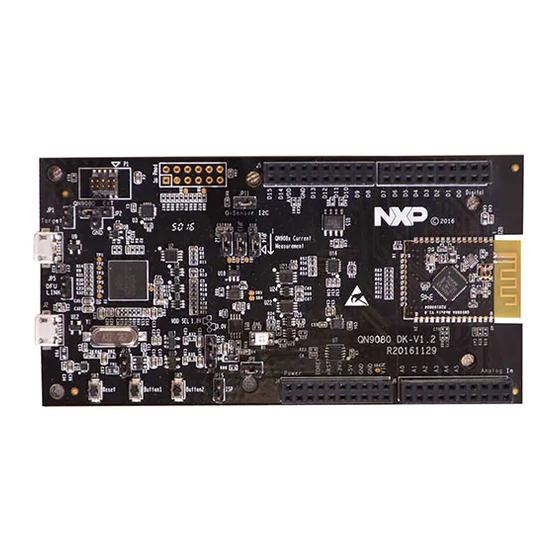
QN908x NXP Semiconductors DK User’s Guide 1. Introduction The QN908x DK board is designed for the QN908x HVQFN and WLCSP package IC evaluation and development. It is easy to evaluate QN908x’s functions and performance. There are also some useful peripherals like the GPIOs, PMod, and Arduino interface. -
Page 4: Hardware Description
QN908x NXP Semiconductors DK User’s Guide 2. Hardware description The QN908x DK board provides easy access to peripherals, such as the buttons and LED. The board also provides useful interfaces, such as the USB port for UART communication and CMSIS-DAP debugger, and the standard Arduino & Pmod connector. - Page 5 QN908x NXP Semiconductors DK User’s Guide Table 1. QN908x DK V1.2 board’s mark information list Number Name Description The QN908x USB port provides power supply to the whole QN908x USB port board and the USB signal path to the QN908x module.
-
Page 6: Default Jumper Settings On The Dk Board
QN908x NXP Semiconductors DK User’s Guide 2.2 Default jumper settings on the DK board As shown in 2, the power, JTAG/SWD, UART, and I C enable jumpers are connected by default. Table 2 Table 3 show the jumpers’ functions and how to set them. -
Page 7: Qn9080 Module
QN908x NXP Semiconductors DK User’s Guide Fig 3. Debugger connector 2.4 QN908x module The QN908x IC integrates the BLE radio, controller, protocol stack, and profile software on a single chip, which provides a flexible and easy way to use the BLE SoC solution. It ®... -
Page 8: Gpio And Arduino Interfaces
QN908x NXP Semiconductors DK User’s Guide 2.5 GPIO and Arduino interfaces On the QN908x DK board, the J4, J5, J6, and J7 connectors all provide GPIO connection outputs. The board is also compatible with the Arduino board interface. The interface schematic is shown in Fig 5. -
Page 9: Jtag Interface
QN908x NXP Semiconductors DK User’s Guide 2.8 SWD/JTAG interface The board provides a SWD/JTAG interface to be used by an external debugger, as shown in Fig 8. Debugger interface 2.9 Buttons As shown in 9, the DK board offers three buttons. When using the SW1 and SW2 buttons, the GPIO must be configured as the input. -
Page 10: Board Application Function
QN908x NXP Semiconductors DK User’s Guide 3. DK board application function 3.1 CMSIS-DAP interface The QN908x DK V1.2 board offers the JTAG/SWD interface either to the on-board or off-board QN908x targets. It also provides the USB-to-UART interface for QN908x. To change to the CMSIS-DAP interface, see Chapter 4.4 in UM11097. - Page 11 QN908x NXP Semiconductors DK User’s Guide 3.2.1 Current test using LPC4322 The QN908x DK board has an on-board current measurement circuit consisting of the MAX9634T (U18) current monitor chip and the 12-bit ADC (ADC122S021, U19) with a 12-bit sampling from 50 ksps to 200 ksps. The on-board MAX9634T current monitor measures the voltage across the QN908x VCC V-sense resistors;...
- Page 12 QN908x NXP Semiconductors DK User’s Guide 3.2.2 Current test using a digital ammeter When performing the current test using an external digital ammeter, jumpers JP12, JP13, and JP14 must be set according to Table 7. Use a jumper cap to short the pins. The schematic is shown in Fig 13.
-
Page 13: Rf Connective Test With Cbt
QN908x NXP Semiconductors DK User’s Guide 3.3 RF connective test with CBT The QN908x module RF signal can be tested by the on-trace RF connector. This RF connector is manufactured by Murata. When performing the RF test with the CBT instruments system, you may need an expansion board to match the signal voltage level from UART to the RS232 interface. -
Page 14: Dongle Connection
QN908x NXP Semiconductors DK User’s Guide Fig 17. Connection as virtual COM port 4.2 Dongle connection The QN9080 USB dongle is a USB-interfaced device with the QN9080 built in. With the driver and SDK installed on your computer (See Chapter 4.2 in document UM11097), use the Connectivity QTool in SDK to control the QN9080 in the dongle to work as a central/peripheral device. - Page 15 QN908x NXP Semiconductors DK User’s Guide Fig 18. Power schematic of the QN908x DK board Fig 19. LPC processor schematic of the QN908x DK board QN908x-DK All information provided in this document is subject to legal disclaimers. © NXP B.V. 2018. All rights reserved.
- Page 16 QN908x NXP Semiconductors DK User’s Guide Fig 20. QN908x-BLE schematic of the QN908x DK board Fig 21. QN908x-function schematic of the QN908x DK board QN908x-DK All information provided in this document is subject to legal disclaimers. © NXP B.V. 2018. All rights reserved.
- Page 17 QN908x NXP Semiconductors DK User’s Guide Fig 22. Arduino interface schematic of the QN908x DK board 5.1.2 QN9080 module board Fig 23. QN9080 QFN module board QN908x-DK All information provided in this document is subject to legal disclaimers. © NXP B.V. 2018. All rights reserved.
-
Page 18: Pcb Layout
QN908x NXP Semiconductors DK User’s Guide 5.2 PCB layout 5.2.1 QN908x DK main board Fig 24. Top etch Fig 25. GND plane QN908x-DK All information provided in this document is subject to legal disclaimers. © NXP B.V. 2018. All rights reserved. - Page 19 QN908x NXP Semiconductors DK User’s Guide Fig 26. PWR plane Fig 27. Top silkscreen QN908x-DK All information provided in this document is subject to legal disclaimers. © NXP B.V. 2018. All rights reserved. User’s Guide Rev. 1.2 — April 2018...
- Page 20 QN908x NXP Semiconductors DK User’s Guide Fig 28. Bottom silkscreen 5.2.2 QN9080 QFN board Fig 29. Top etch QN908x-DK All information provided in this document is subject to legal disclaimers. © NXP B.V. 2018. All rights reserved. User’s Guide Rev. 1.2 — April 2018...
- Page 21 QN908x NXP Semiconductors DK User’s Guide Fig 30. GND plane Fig 31. PWR plane QN908x-DK All information provided in this document is subject to legal disclaimers. © NXP B.V. 2018. All rights reserved. User’s Guide Rev. 1.2 — April 2018...
- Page 22 QN908x NXP Semiconductors DK User’s Guide Fig 32. Bottom etch Fig 33. Top silkscreen QN908x-DK All information provided in this document is subject to legal disclaimers. © NXP B.V. 2018. All rights reserved. User’s Guide Rev. 1.2 — April 2018...
-
Page 23: Dimensions Of The Pcb Board
QN908x NXP Semiconductors DK User’s Guide 5.3 Dimensions of the PCB board 5.3.1 QN908x DK board Fig 34. Dimensions of the QN908x DK board QN908x-DK All information provided in this document is subject to legal disclaimers. © NXP B.V. 2018. All rights reserved. -
Page 24: Notes For Using A Lithium Battery
QN908x NXP Semiconductors DK User’s Guide 5.3.2 QN9080 QFN module Fig 35. Dimensions of the QN9080 QFN module board 5.4 Notes for using a lithium battery When using a lithium battery as the power supply for the QN9080 module, pay attention to the following: ... -
Page 25: Statements
QN908x NXP Semiconductors DK User’s Guide 5.5 Statements 5.5.1 FCC compliance statement Changes or modifications not expressly approved by the party responsible for compliance could void the user's authority to operate the equipment. This equipment has been tested and found to comply with the limits for a Class B digital device, pursuant to Part 15 of the FCC Rules. -
Page 26: Legal Information
In no event shall NXP Semiconductors be liable for any indirect, incidental, punitive, special or consequential damages (including - without limitation -... -
Page 27: Table Of Contents
QN908x NXP Semiconductors DK User’s Guide 7. Contents Introduction ............3 Purpose .............. 3 Kit contents ............3 Hardware description .......... 4 Hardware overview ..........4 Default jumper settings on the DK board ... 6 CMSIS-DAP debugger ........6 QN9080 module ..........7 GPIO and Arduino interfaces ...... - Page 28 Mouser Electronics Authorized Distributor Click to View Pricing, Inventory, Delivery & Lifecycle Information: QN9080-DK...
Need help?
Do you have a question about the QN908 Series and is the answer not in the manual?
Questions and answers