Table of Contents
Advertisement
Quick Links
www.ti.com
User's Guide
JFE150 Evaluation Module
This user's guide contains information and support documentation for the JFE150 evaluation module (EVM).
Included are the circuit description, schematic, and bill of materials of the JFE150EVM. Throughout this
document, the terms evaluation board, evaluation module, and EVM are synonymous with the JFE150EVM.
SLPU009 – FEBRUARY 2022
Submit Document Feedback
ABSTRACT
Copyright © 2022 Texas Instruments Incorporated
JFE150 Evaluation Module
1
Advertisement
Table of Contents

Subscribe to Our Youtube Channel
Related Manuals for Texas Instruments JFE150


Summary of Contents for Texas Instruments JFE150
- Page 1 JFE150 Evaluation Module ABSTRACT This user's guide contains information and support documentation for the JFE150 evaluation module (EVM). Included are the circuit description, schematic, and bill of materials of the JFE150EVM. Throughout this document, the terms evaluation board, evaluation module, and EVM are synonymous with the JFE150EVM.
-
Page 2: Table Of Contents
4.1 JFE150EVM Schematic..............................4.2 PCB Layout..................................4.3 Bill of Materials.................................14 List of Figures Figure 3-1. Pre-Amp With JFE150 Front End in a Closed-Loop Circuit..................Figure 3-2. Gain vs Frequency..............................Figure 4-1. JFE150EVM Default Configuration Schematic......................6 Figure 4-2. JFE150EVM Power Supply Connections........................ -
Page 3: Overview
N-channel JFET capable of operating over a wide drain-to- source voltage of up to 40 V and a gate-to-drain voltage down to –40 V. The JFE150 yields excellent noise performance for currents from 50 μA to 20 mA with extremely high input impedance (> 1 TΩ). When biased at 5 mA, the device yields 0.8 nV/√Hz. -
Page 4: Getting Started
Figure 4-2. If dual-supply operation is required, VSS can be powered separately; adjust components R25 and R12 to bias the JFE150 to the desired bias point. Set Vbias to midsupply, as discussed in section Section 2.3. 2.2 Input The input to the JFE150EVM is designed to interface high-impedance sources to the gate of the JFET. -
Page 5: Application Circuit
VDD = 12 V and VSS = GND. The output voltage, Vout, settles to approximately midsupply or 6 V, as shown in Figure 3-1. A theoretical explanation of the preamplifier with a JFE150 front end in a closed-loop circuit is detailed in the JFE150 Ultra-Low-Noise- Pre-Amp application report. -
Page 6: Schematic, Pcb Layout, And Bill Of Materials
10.0k 1.00M 470uF 1.00M Vbias 110k Vbias Vbias 110k VS Bias 10µF 100nF 110k 100nF 10µF OPA202ID JFE150DCK Figure 4-1. JFE150EVM Default Configuration Schematic JFE150 Evaluation Module SLPU009 – FEBRUARY 2022 Submit Document Feedback Copyright © 2022 Texas Instruments Incorporated... -
Page 7: Figure 4-2. Jfe150Evm Power Supply Connections
Schematic, PCB Layout, and Bill of Materials 100uF 100uF Figure 4-2. JFE150EVM Power Supply Connections SLPU009 – FEBRUARY 2022 JFE150 Evaluation Module Submit Document Feedback Copyright © 2022 Texas Instruments Incorporated... -
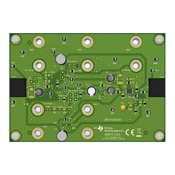
Page 8: Pcb Layout
Schematic, PCB Layout, and Bill of Materials www.ti.com 4.2 PCB Layout Figure 4-3. JFE150EVM PCB Layout Figure 4-4. JFE150EVM Top Overlay JFE150 Evaluation Module SLPU009 – FEBRUARY 2022 Submit Document Feedback Copyright © 2022 Texas Instruments Incorporated... -
Page 9: Figure 4-5. Jfe150Evm Top Solder Mask
Schematic, PCB Layout, and Bill of Materials Figure 4-5. JFE150EVM Top Solder Mask Figure 4-6. JFE150EVM Top Layer SLPU009 – FEBRUARY 2022 JFE150 Evaluation Module Submit Document Feedback Copyright © 2022 Texas Instruments Incorporated... -
Page 10: Figure 4-7. Jfe150Evm Signal Layer 1
Schematic, PCB Layout, and Bill of Materials www.ti.com Figure 4-7. JFE150EVM Signal Layer 1 Figure 4-8. JFE150EVM Signal Layer 2 JFE150 Evaluation Module SLPU009 – FEBRUARY 2022 Submit Document Feedback Copyright © 2022 Texas Instruments Incorporated... -
Page 11: Figure 4-9. Jfe150Evm Bottom Layer
Schematic, PCB Layout, and Bill of Materials Figure 4-9. JFE150EVM Bottom Layer Figure 4-10. JFE150EVM Bottom Solder Mask SLPU009 – FEBRUARY 2022 JFE150 Evaluation Module Submit Document Feedback Copyright © 2022 Texas Instruments Incorporated... -
Page 12: Figure 4-11. Jfe150Evm Bottom Overlay
Schematic, PCB Layout, and Bill of Materials www.ti.com Figure 4-11. JFE150EVM Bottom Overlay Figure 4-12. JFE150EVM Drill Drawing JFE150 Evaluation Module SLPU009 – FEBRUARY 2022 Submit Document Feedback Copyright © 2022 Texas Instruments Incorporated... -
Page 13: Figure 4-13. Jfe150Evm Board Dimensions
Schematic, PCB Layout, and Bill of Materials Figure 4-13. JFE150EVM Board Dimensions SLPU009 – FEBRUARY 2022 JFE150 Evaluation Module Submit Document Feedback Copyright © 2022 Texas Instruments Incorporated... -
Page 14: Bill Of Materials
RES, 110 k, 0.1%, 0.125 W, 0805 RG2012P-114-B-T5 Susumu Co Ltd R18, R20, R22, R23, RES SMD 0 OHM JUMPER 1/8W 0805 RC0805FR-070RL Yageo R25, R26, R27 JFE150 Evaluation Module SLPU009 – FEBRUARY 2022 Submit Document Feedback Copyright © 2022 Texas Instruments Incorporated... - Page 15 Panasonic Electronic Resistor 0805 (2012 Metric) Automotive Components AEC-Q200 Thin Film R28, R29, R30, R31 RES SMD 0 OHM JUMPER 1/8W 0805 RC0805FR-070RL Yageo SLPU009 – FEBRUARY 2022 JFE150 Evaluation Module Submit Document Feedback Copyright © 2022 Texas Instruments Incorporated...
- Page 16 STANDARD TERMS FOR EVALUATION MODULES Delivery: TI delivers TI evaluation boards, kits, or modules, including any accompanying demonstration software, components, and/or documentation which may be provided together or separately (collectively, an “EVM” or “EVMs”) to the User (“User”) in accordance with the terms set forth herein.
- Page 17 www.ti.com Regulatory Notices: 3.1 United States 3.1.1 Notice applicable to EVMs not FCC-Approved: FCC NOTICE: This kit is designed to allow product developers to evaluate electronic components, circuitry, or software associated with the kit to determine whether to incorporate such items in a finished product and software developers to write software applications for use with the end product.
- Page 18 www.ti.com Concernant les EVMs avec antennes détachables Conformément à la réglementation d'Industrie Canada, le présent émetteur radio peut fonctionner avec une antenne d'un type et d'un gain maximal (ou inférieur) approuvé pour l'émetteur par Industrie Canada. Dans le but de réduire les risques de brouillage radioélectrique à...
- Page 19 www.ti.com EVM Use Restrictions and Warnings: 4.1 EVMS ARE NOT FOR USE IN FUNCTIONAL SAFETY AND/OR SAFETY CRITICAL EVALUATIONS, INCLUDING BUT NOT LIMITED TO EVALUATIONS OF LIFE SUPPORT APPLICATIONS. 4.2 User must read and apply the user guide and other available documentation provided by TI regarding the EVM prior to handling or using the EVM, including without limitation any warning or restriction notices.
- Page 20 Notwithstanding the foregoing, any judgment may be enforced in any United States or foreign court, and TI may seek injunctive relief in any United States or foreign court. Mailing Address: Texas Instruments, Post Office Box 655303, Dallas, Texas 75265 Copyright © 2019, Texas Instruments Incorporated...
- Page 21 TI products. TI’s provision of these resources does not expand or otherwise alter TI’s applicable warranties or warranty disclaimers for TI products. TI objects to and rejects any additional or different terms you may have proposed. IMPORTANT NOTICE Mailing Address: Texas Instruments, Post Office Box 655303, Dallas, Texas 75265 Copyright © 2022, Texas Instruments Incorporated...
- Page 22 Mouser Electronics Authorized Distributor Click to View Pricing, Inventory, Delivery & Lifecycle Information: Texas Instruments JFE150EVM...
Need help?
Do you have a question about the JFE150 and is the answer not in the manual?
Questions and answers