Table of Contents
Advertisement
Quick Links
TSW14J56 JESD204B High-Speed Data Capture and
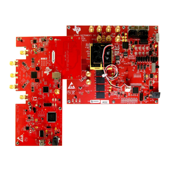
The TI TSW14J56 evaluation module (EVM) is a next generation pattern generator and data capture card
used to evaluate performances of the new TI JESD204B device family of high-speed analog-to-digital
converters (ADC) and digital-to-analog converters (DAC). For an ADC, by capturing the sampled data over
a JESD204B interface when using a high-quality, low-jitter clock, and a high-quality input frequency, the
TSW14J56 can be used to demonstrate datasheet performance specifications. Using Altera JESD204B IP
cores, the TSW14J56 can be dynamically configurable to support lane speeds from 600 Mbps to 12.5
Gbps, from 1 to 8 lanes, 1 to 16 converters, and 1 to 4 octets per frame with one firmware build. Together
with the accompanying
system that captures and evaluates data samples from ADC EVMs and generates and sends desired test
patterns to DAC EVMs.
Trademarks
Windows is a trademark of Microsoft Corporation.
1
Functionality
The TSW14J56EVM has a single industry standard FMC connector that interfaces directly with TI
JESD204B ADC and DAC EVM's. When used with an ADC EVM, high-speed serial data is captured, de-
serialized and formatted by an Altera Arria V GZ FPGA. The data is then stored into an external DDR3
memory bank, enabling the TSW14J56 to store up to 2G 16-bit data samples. To acquire data on a host
PC, the FPGA reads the data from memory and transmits it on a high speed 32 bit parallel interface. An
onboard high-speed USB 3.0 to parallel converter bridges the FPGA interface to the host PC and GUI.
In pattern generator mode, the TSW14J56 generates desired test patterns for DAC EVMs under test.
These patterns are sent from the host PC over the USB interface to the TSW14J56. The FPGA stores the
data received into the board DDR3 memory module. The data from memory is then read by the FPGA and
transmitted to a DAC EVM across the JESD204B interface connector. The board contains a 100-MHz
oscillator used to generate the DDR3 reference clock and a option for a 10-MHz oscillator for general
purpose use.
Figure 1
SLWU086C – November 2013 – Revised January 2016
Submit Documentation Feedback
Pattern Generator Card User's Guide
High-Speed Data Converter Pro Graphic User Interface
shows the TI ADS58J63EVM plugged into the TSW14J56EVM.
TSW14J56 JESD204B High-Speed Data Capture and Pattern Generator
Copyright © 2013–2016, Texas Instruments Incorporated
SLWU086C – November 2013 – Revised January 2016
User's Guide
(GUI), it is a complete
1
Card User's Guide
Advertisement
Table of Contents

Related Manuals for Texas Instruments TSW14J56


Summary of Contents for Texas Instruments TSW14J56
- Page 1 Altera Arria V GZ FPGA. The data is then stored into an external DDR3 memory bank, enabling the TSW14J56 to store up to 2G 16-bit data samples. To acquire data on a host PC, the FPGA reads the data from memory and transmits it on a high speed 32 bit parallel interface. An onboard high-speed USB 3.0 to parallel converter bridges the FPGA interface to the host PC and GUI.
- Page 2 • Supported by TI HSDC PRO software • FPGA firmware developed with Quartus II 14.0 and QSYS TSW14J56 JESD204B High-Speed Data Capture and Pattern Generator SLWU086C – November 2013 – Revised January 2016 Card User's Guide Submit Documentation Feedback Copyright © 2013–2016, Texas Instruments Incorporated...
- Page 3 Character replacement enabled or disabled through USB and JTAG – Dynamically reconfigurable transceiver data rate. Operating range from 0.600 to 12.5 Gbps Figure 2 shows a block diagram of the TSW14J56 EVM. TSW14J56 EVM +5 VDC Input 32Gb DDR III...
-
Page 4: Hardware Configuration
ADC JESD interface configured for 4 lanes, 2 converters, and 1 octet per frame. The TSW14J56 device can capture up to 2G 16-bit samples at a maximum line rate of 12.5 Gbps that are stored inside the on-board DDR3 memory. To acquire data on a host PC, the FPGA reads the data from memory and transmits parallel data to the on-board high-speed parallel-to-USB converter. -
Page 5: Switches And Pushbuttons
Power monitor U13 reset 2.2.2 Jumpers The TSW14J56 contains several jumpers (JP) and solder jumpers (SJP) that enable certain functions on the board. The description of the jumpers can be found in Table Table 2. Jumper Description of the TSW14J56 Device... - Page 6 LEDs 2.3.1 Power and Configuration LEDs Several LEDs are on the TSW14J56 EVM to indicate the presence of power and the state of the FPGA. The description of these LEDs can be found in Table Table 3. Power and Configuration LED Description of the TSW14J56 Device...
- Page 7 2.3.3.2 FPGA Mezzanine Card (FMC) Connector The TSW14J56 EVM has one connector to allow for the direct plug in of TI JESD204B serial interface ADC and DAC EVMs. The specifications for this connector are mostly derived from the ANSI/VITA 57.1 FPGA Mezzanine Card (FMC) Standard.
- Page 8 The ANSI/VITA 57.1 standard assigns voltages to certain pins. These are labeled as 12V, 3P3V, and VADJ nets on the connector page of the schematic. On the TSW14J56, these pins are connected to test points to allow the user to provide voltages at these pin locations.
- Page 9 FPGA configuration file, capture data from ADC EVMs, and send test pattern data to the DAC EVMs. SLWU086C – November 2013 – Revised January 2016 TSW14J56 JESD204B High-Speed Data Capture and Pattern Generator Card User's Guide Submit Documentation Feedback...
-
Page 10: Software Start-Up
4. The user can connect several TSW14J56 EVMs to one host PC, but the GUI can only connect to one at a time. When multiple boards are connected to the PC, the pop-up displays all of the serial numbers found. The user then selects which board to associate the GUI with. - Page 11 USB port. When the software is installed and the USB cable is connected to the TSW14J56EVM and the PC, the TSW14J56 USB 3.0 converter should be located in the Hardware Device Manager under the universal serial bus controllers as shown in Figure 6 labeled as Cypress FX3 USB StreamerExample Device.
-
Page 12: Downloading Firmware
FPGA_CONF_DONE LED (D28) illuminates along with several of the status LEDs. Figure 7. Select ADC Firmware to be Loaded TSW14J56 JESD204B High-Speed Data Capture and Pattern Generator SLWU086C – November 2013 – Revised January 2016 Card User's Guide Submit Documentation Feedback Copyright ©... - Page 13 Figure 8. Download Firmware Error Message SLWU086C – November 2013 – Revised January 2016 TSW14J56 JESD204B High-Speed Data Capture and Pattern Generator Card User's Guide Submit Documentation Feedback Copyright © 2013–2016, Texas Instruments Incorporated...
-
Page 14: Revision History
Changes from A Revision (November 2013) to B Revision ................... Page ............• Changed TSW14J56EVM Interfacing with an ADS42JB49EVM image..................• Changed TSW14J56 EVM Block Diagram image..................• Changed TSW14J56EVM Serial Number image..............• Changed High-Speed Data Converter Pro GUI Top Level image.................. - Page 15 IMPORTANT NOTICE FOR TI DESIGN INFORMATION AND RESOURCES Texas Instruments Incorporated (‘TI”) technical, application or other design advice, services or information, including, but not limited to, reference designs and materials relating to evaluation modules, (collectively, “TI Resources”) are intended to assist designers who are developing applications that incorporate TI products;...
- Page 16 Mouser Electronics Authorized Distributor Click to View Pricing, Inventory, Delivery & Lifecycle Information: Texas Instruments TSW14J56EVM...
Need help?
Do you have a question about the TSW14J56 and is the answer not in the manual?
Questions and answers