Renesas RL78/L12 User Manual
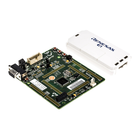
Starter kit
Hide thumbs
Also See for RL78/L12:
- User manual (55 pages) ,
- User manual (58 pages) ,
- User manual (59 pages)
Table of Contents
Advertisement
Quick Links
RL78/L12 Group
32
16
RENESAS MCU
RL78 Family / L1X Series
All information contained in these materials, including products and product specifications, represents
information on the product at the time of publication and is subject to change by Renesas Electronics
Corporation without notice. Please review the latest information published by Renesas Electronics
Corporation through various means, including the Renesas Electronics Corporation website
(http://www.renesas.com).
Renesas Starter Kit User's Manual
For CubeSuite+
Rev. 1.00 Jan 2013
Advertisement
Table of Contents

Related Manuals for Renesas RL78/L12


Summary of Contents for Renesas RL78/L12
- Page 1 All information contained in these materials, including products and product specifications, represents information on the product at the time of publication and is subject to change by Renesas Electronics Corporation without notice. Please review the latest information published by Renesas Electronics Corporation through various means, including the Renesas Electronics Corporation website (http://www.renesas.com).
- Page 2 Electronics product for any application for which it is not intended. Renesas Electronics shall not be in any way liable for any damages or losses incurred by you or third parties arising from the use of any Renesas Electronics product for which the product is not intended by Renesas Electronics.
- Page 3 RSK. Renesas expressly disclaims all such warranties. Renesas or its affiliates shall in no event be liable for any loss of profit, loss of data, loss of contract, loss of business, damage to reputation or goodwill, any economic loss, any reprogramming or recall...
- Page 4 The revision history summarizes the locations of revisions and additions. It does not list all revisions. Refer to the text of the manual for details. The following documents apply to the RL78/L12 Group. Make sure to refer to the latest versions of these documents. The newest versions of the documents listed may be obtained from the Renesas Electronics Web site.
- Page 5 Electromagnetic Compatibility Electrostatic Discharge Philips™ Inter-Integrated Circuit Connection Bus Interrupt Request Liquid Crystal Display Light Emitting Diode Micro-controller Unit Personal Computer Pulse Width Modulation Renesas Starter Kit Serial Array Unit Special Function Register UART Universal Asynchronous Receiver/Transmitter Universal Serial Bus...
-
Page 6: Table Of Contents
Table of Contents 1. Overview ..........................7 Purpose ..............................7 Features ..............................7 2. Power Supply ........................8 Requirements ............................. 8 Power-Up Behaviour ..........................8 3. Board Layout ........................9 Component Layout ............................. 9 Board Dimensions ............................ 10 Component Placement ..........................11 4. -
Page 7: Overview
Jan 15, 2013 1. Overview Purpose This RSK is an evaluation tool for Renesas microcontrollers. This manual describes the technical details of the RSK hardware. The Quick Start Guide and Tutorial Manual provide details of the software installation and debugging environment. -
Page 8: Power Supply
When the RSK is purchased, the RSK board has the ‘Release’ or stand-alone code from the example tutorial software pre-programmed into the Renesas microcontroller. On powering up the board the LCD panel segments will start to flash. After 200 flashes or after pressing any switch, the text on the display will change and the heart symbol will begin to flash at a rate controlled by the potentiometer. -
Page 9: Board Layout
RSKRL78L12 3. Board Layout 3. Board Layout Component Layout Figure 3-1 below shows the top component layout of the board. Application Headers Reset Switch RS232 Serial Debug LCD Power Jack connector Power LED E1 Interface RL78L12 User LEDs User Switches Application Headers Potentiometer Figure 3-1: Board Layout... -
Page 10: Board Dimensions
RSKRL78L12 3. Board Layout Board Dimensions Figure 3-2 below gives the board dimensions and connector positions. All the through-hole connectors are on a common 0.1 inch grid for easy interfacing. 7.0mm 3.2mm 3.00mm 13.88mm 45.00mm RL78L12 27.00mm 43.18mm 48.26mm 50.80mm 55.88mm 86.36mm 99.06mm... -
Page 11: Component Placement
RSKRL78L12 3. Board Layout Component Placement Figure 3-3 below shows placement of individual components on the top-side PCB. Component types and values can be looked up using the board schematics. POWER LED0 LED1 LED2 LED3 R11 R12 R13 R14 R15 R131 R123 R125... -
Page 12: Connectivity
RSKRL78L12 Connectivity 4. Connectivity Internal RSK Connections The diagram below shows the RSK board components and their connectivity to the MCU. MCU Current Power Jack Draw Test Point Application Headers Micon Pin Header RL78L12 LCD Panel Reset E1 Debug Interface RS-232 Serial Port Debug LCD RESET... -
Page 13: Debugger Connections
RSKRL78L12 Connectivity Debugger Connections The diagram below shows the connections between the RSK, E1 debugger and the host PC. User Interface USB Cable Cable E1 Emulator Host PC Figure 4-2: Debugger Connection Diagram R20UT0922EG0100 Rev. 1.00 Page 13 of 41 Jan 15, 2013... -
Page 14: User Circuitry
A clock circuit is fitted to the RSK to generate the required clock signal to drive the MCU, and associated peripherals. Refer to the RL78/L12 Group Hardware Manual for details regarding the clock signal requirements, and the RSKRL78L12 board schematics for information regarding the clock circuitry in use on Table 5-1 the RSK. -
Page 15: Leds
Board_VDD and ground. The potentiometer is fitted to offer an easy method of supplying a variable analog input to the microcontroller. It does not necessarily reflect the accuracy of the controller’s ADC. Refer to the RL78/L12 Group Hardware Manual for further details. -
Page 16: Lcd Panel
RSKRL78L12 User Circuitry LCD Panel A versatile LCD display panel is supplied with the RSK, and should be connected to the JA4 header. The panel is directly driven by circuitry inside the MCU. Connection information for the LCD panel is provided Table 5-4 in table below. -
Page 17: Debug Lcd Module
RSKRL78L12 User Circuitry Debug LCD Module A debug LCD header is fitted to the RSK; however the two-line debug LCD is not supplied with this kit. It is not possible to use the debug LCD and the LCD panel at the same time, and they should not both be fitted to the RSK. -
Page 18: Rs232 Serial Port
RSKRL78L12 User Circuitry RS232 Serial Port An RS232 serial port is fitted to the RSK and connected via a level shifter to the microcontroller Serial Array Unit (SAU). Connections between the RS232 header and the microcontroller are listed in Table 5-6 below. -
Page 19: Configuration
When modifying a link resistor, always check the related option links to ensure there is no possible signal contention or short circuits. Because some of the MCU’s pins are multiplexed, some of the peripherals must be used exclusively. Refer to the RL78/L12 Group Hardware Manual and RSKRL78L12 board schematics for further information. ADC Configuration Table 6-1 below details the function of the option links associated with the Analog-to-Digital circuit. -
Page 20: E1 Debugger Interface
RSKRL78L12 Configuration E1 Debugger Interface Table 6-2 below details the function of the option links associated with serial port configuration. Reference Link Fitted Configuration Link Removed Configuration Related Ref. Connects U4 (Y, pin 4) to the MCU Disconnects U4 (Y, pin 4) from the (RESET, pin 6) MCU (RESET, pin 6) Connects TRESET (E1, pin 6) to the... -
Page 21: Rs232 Serial Port Configuration
RSKRL78L12 Configuration RS232 Serial Port Configuration Table 6-3 below details the function of the option links associated with serial port configuration. Reference Link Fitted Configuration Link Removed Configuration Related Ref. Connects the serial port connector Disconnects serial port shield to Ground. connector shield from Ground. -
Page 22: Irq & General I/O Pin Configuration
RSKRL78L12 Configuration IRQ & General I/O Pin Configuration Table 6-4 below details the function of the option links associated with IRQ and general I/O pin configuration. Reference Link Fitted Configuration Link Removed Configuration Related Ref. Connects the MCU (SCK00n, pin 62) Disconnects the MCU (SCK00n, pin 62) to SCK00n (JA2, pin 10). -
Page 23: User Switch Configuration
RSKRL78L12 Configuration User Switch Configuration Table 6-5 below details the function of the option links associated with the user switches. Reference Link Fitted Configuration Link Removed Configuration Related Ref. Connects the switch SW1 to the MCU Disconnects the switch SW1 from the (INTP0, pin 9) MCU (INTP0, pin 9) Connects the switch SW2 to the MCU... -
Page 24: Power Supply Configuration
RSKRL78L12 Configuration Power Supply Configuration Table 6-8 below details the function of the option links associated with power supply configuration. Reference Link Fitted Configuration Link Removed Configuration Related Ref. Connects the power socket (PWR pin) Disconnects the Power socket (PWR to the voltage regulator (U2, pin 3) pin) from the voltage regulator (U2, and Board_5V. -
Page 25: Clock Configuration
RSKRL78L12 Configuration Clock Configuration Table 6-10 below details the function of the option links associated with clock configuration. Reference Link Fitted Configuration Link Removed Configuration Related Ref. Connects the crystal X1 to the MCU Disconnects the crystal X1 from the (X2, pin 10). -
Page 26: Lcd Panel Configuration
RSKRL78L12 Configuration 6.10 LCD Panel Configuration Table 6-11 below details the function of the option links associated with LCD panel configuration. Reference Link Fitted Configuration Link Removed Configuration Related Ref. Connects the LCD panel (JA4, pin 1) to Disconnects the LCD panel (JA4, R132 Board_VDD. - Page 27 RSKRL78L12 Configuration Reference Link Fitted Configuration Link Removed Configuration Related Ref. Connects the MCU (SEG14, pin 30) to Disconnects the MCU (SEG14, pin the LCD panel (JA4, pin 25) and the 30) from the LCD panel (JA4, pin 25) debug LCD header (pin 13). and the debug LCD header (pin 13).
-
Page 28: Headers
7. Headers Application Headers This RSK is fitted with application headers, which can be used to connect compatible Renesas application devices or as easy access to MCU pins. Note that JA4 has been omitted from this list as it is the LCD panel connector, and connections are described in §5.6... - Page 29 RSKRL78L12 7. Headers Table 7-2 below lists the connections of the application header, JA2. Application Header JA2 Circuit Net Name MCU Pin Circuit Net Name MCU Pin RESETn CON_X2 10 (via R3) GROUND TxD0 60 (via J11/R65) RxD0 61 (via J10/R64) INTP3 26 (via R77) SCK00n...
- Page 30 RSKRL78L12 7. Headers Table 7-3 below lists the connections of the application header, JA5. Application Header JA5 Circuit Net Name MCU Pin Circuit Net Name MCU Pin ANI20 57 (via R111) ANI21 56 (via R113) ANI22 55 (via R115) ANI23 54 (via R117) Table 7-3: Application Header JA5 Connections Table 7-4 below lists the connections of the application header, JA6.
-
Page 31: Microcontroller Pin Headers
RSKRL78L12 7. Headers Microcontroller Pin Headers This RSK is fitted with MCU pin headers, which are used to access all the MCU’s pins. Table 7-5 below lists the connections of the microcontroller pin header, J1. Microcontroller Pin Header J1 Circuit Net Name MCU Pin Circuit Net Name MCU Pin... - Page 32 RSKRL78L12 7. Headers Table 7-6 below lists the connections of the microcontroller pin header, J2. Microcontroller Pin Header J2 Circuit Net Name MCU Pin Circuit Net Name MCU Pin SEG21_SCLA0 SEG20_SDAA0 CAPH CAPL SEG19_LED0 SEG18_INTP3 SEG17_INTP4 SEG16_DLCDD4_IO0 SEG15_DLCDD5_IO1 SEG14_DLCDD6_IO2 SEG13_DLCDD7_IO3 SEG12_IO4 Table 7-6: Microcontroller Pin Header J2 Connections R20UT0922EG0100 Rev.
- Page 33 RSKRL78L12 7. Headers Table 7-7 below lists the connections of the microcontroller pin header, J3. Microcontroller Pin Header J3 Circuit Net Name MCU Pin Circuit Net Name MCU Pin SEG11_IO5 SEG10_TI07 SEG9_LED3 SEG8_LED2_TO06 SEG7_DLCDRS SEG6_SO01 SEG5_SIO1 SEG4_SCK01n SEG3 SEG2 SEG1 SEG0 COM3 COM2...
- Page 34 RSKRL78L12 7. Headers Table 7-8 below lists the connections of the microcontroller pin header, J4. Microcontroller Pin Header J4 Circuit Net Name MCU Pin Circuit Net Name MCU Pin AVREFM ADPOT_AVREFP DLCDE SEG38_IO7 SEG37_IO6 SEG36_ANI23 SEG35_ANI22 SEG34_ANI21 SEG33_ANI20_SW3 SEG32_ANI19_SW2 SEG31_ANI18 SEG30_TxD0 SEG29_RxD0 SEG28_SCK00n...
-
Page 35: Code Development
8. Code Development Overview For all code debugging using Renesas software tools, the RSK board must be connected to a PC via an E1/E20 debugger. An E1 debugger is supplied with this RSK product. For further information regarding the debugging capabilities of the E1/E20 debuggers, refer to E1/E20 Emulator Additional Document for User's Manual (R20UT1994EJ). -
Page 36: Address Space
Address Space Figure 8-1 below details the address space of the MCU. The MCU fitted to the RSK has 32KB of ROM. For further details, refer to the RL78/L12 Group Hardware Manual. Figure 8-1: MCU Address Space Diagram R20UT0922EG0100 Rev. 1.00... -
Page 37: Additional Information
Copyright This document may be, wholly or partially, subject to change without notice. All rights reserved. Duplication of this document, either in whole or part is prohibited without the written permission of Renesas Electronics Europe Limited. © 2013 Renesas Electronics Europe Limited. All rights reserved. - Page 38 REVISION HISTORY RSKRL78L12 User’s Manual Rev. Date Description Page Summary 1.00 Jan 15, 2013 First Edition issued...
- Page 39 Renesas Starter Kit Manual: User’s Manual Publication Date: Rev. 1.00 Jan 15, 2013 Published by: Renesas Electronics Corporation...
- Page 40 SALES OFFICES Refer to "http://www.renesas.com/" for the latest and detailed information. Renesas Electronics America Inc. 2880 Scott Boulevard Santa Clara, CA 95050-2554, U.S.A. Tel: +1-408-588-6000, Fax: +1-408-588-6130 Renesas Electronics Canada Limited 1101 Nicholson Road, Newmarket, Ontario L3Y 9C3, Canada...
- Page 41 RL78/L12 Group R20UT0922EG0100...
- Page 42 Mouser Electronics Authorized Distributor Click to View Pricing, Inventory, Delivery & Lifecycle Information: Renesas Electronics R0K5010RLS900BE#WS...
Need help?
Do you have a question about the RL78/L12 and is the answer not in the manual?
Questions and answers