Table of Contents
Advertisement
Quick Links
HIM-15020
Document No.
4
S20284
3
S19692
2
S18805
1
S16335
Rev.
ECN
Confidential C
NOVASTACK
Part No.20697-0**E-0※※, 20698-0**E-0※※
Instruction Manual
June 9, 2020
November 8, 2019
December 26, 2018
June 2, 2016
Date
35-HDP
®
T.Yayoshi
R.Shioya
R.Shioya
T.Kurachi
Prepared by
I-PEX Inc.
1 / 8
Y.Baba
Y.Baba
Checked by
QKE-DFFDE09-03 REV.8
T.Yamauchi
Y.Shimada
T.Hirakawa
J.Tateishi
Approved by
Advertisement
Table of Contents

Related Manuals for I-PEX NOVASTACK 35-HDP


Summary of Contents for I-PEX NOVASTACK 35-HDP
- Page 1 June 9, 2020 T.Yayoshi T.Yamauchi S19692 November 8, 2019 R.Shioya Y.Baba Y.Shimada S18805 December 26, 2018 R.Shioya Y.Baba T.Hirakawa S16335 June 2, 2016 T.Kurachi J.Tateishi Rev. Date Prepared by Checked by Approved by Confidential C I-PEX Inc. QKE-DFFDE09-03 REV.8 1 / 8...
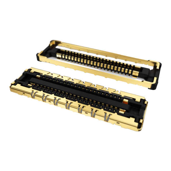
- Page 2 This manual provides the insertion & withdrawal methods and cautions to handle NOVASTACK 35-HDP connector properly. 1. 対象コネクタ名称 型番・部品名/Connector Name, Part number, Part name 1-1. Plug connector 名称/Product Name : NOVASTACK 35-HDP Plug ass'y 型番/Part No. : 20697-0**E-0※※ Contact Power contact...
- Page 3 Document No. NOVASTACK 35-HDP Instruction Manual HIM-15020 ® 1-3. コネクタの方向性に関して/ Connectors Mating Direction 長手方向外郭形状は非対称ですが、Plug ass’y 及び Receptacle ass’y 共に方向性はなく、 どちらの方向に嵌合しても性能への影響はありません。 The ends of the connectors are not identical but the plug and the receptacle can be mated in both ways. The performance of the connector will not be affected by the mating direction of the connectors.
- Page 4 Document No. NOVASTACK 35-HDP Instruction Manual HIM-15020 ® 2-3. 推奨リフロー温度プロファイル Recommended reflow temperature profile (温度はコネクタ端子部付近のプリント基板表面温度) (Temperature: the top surface temperature of the printed circuit board near the connector terminal.) 推奨リフロー温度プロファイル / Recommended Reflow Temperature Profile Confidential C 4 / 8...
- Page 5 Document No. NOVASTACK 35-HDP Instruction Manual HIM-15020 ® 3. 取扱い上の注意 / Cautions for Handling the Component 3-1. 基板-FPC での使用の場合 / Using for board to FPC connection. ① FPC の取り回しによる張力や落下等の衝撃によるコネクタへの負荷に対して、取り回しに 余裕を持たせて頂く事に加え、嵌合方向へ押さえつけて保持をお願い致します。 ① FPC shall not be tensed to withstand in case of a shock or a tension is applied. The FPC shall be fixed toward the mating direction for the maintenance.
- Page 6 Document No. NOVASTACK 35-HDP Instruction Manual HIM-15020 ® 3-2. 基板-基板での使用の場合/ Using for board to board connection. ① 使用される嵌合基板のサイズ・形状によってはコネクタ及びコネクタ半田部への直接負荷による破損 若しくは、振動・衝撃等による嵌合の傾き及び脱落が発生する可能性があります。 コネクタ破損及び嵌合傾き、脱落を防止する為に、スペーサー等を使用した基板間固定を推奨します。 ① To prevent the accidental removal or slant mating, spacers are recommended to fix the space in between the two printed circuit board. There spacers will also help to prevent the damage to the connectors and to the soldered area which might have been caused by the too large printed circuit board or unbalanced shape printed circuit board.
- Page 7 Document No. NOVASTACK 35-HDP Instruction Manual HIM-15020 ® 3-3. コネクタ抜け止め荷重/Press load 嵌合状態のコネクタ抜け止め荷重(筐体で押さえる荷重)につきましては、下記条件でコネクタ上面全体を 押さえる様にして下さい。 (抜け止め荷重:芯数×1.0N 以下) To prevent the coming off of the mated connectors (the load which a connector can apply), press the entire upper surface of the connector with the load calculated in below formula. (Maximum Press load:...
- Page 8 Document No. NOVASTACK 35-HDP Instruction Manual HIM-15020 ® ※注意 2/Caution 2 挿入開始時の奥行き方向のこじり角度は、7°以下でお願いします。 7°以上での挿入は、コネクタ変形の原因となります。 At starting the insertion, please keep the slant 7 degrees or less in direction of depth. By inserting with the slant more than 7 degrees, deformation of the connector will occur. 7°MAX ※注意...
Need help?
Do you have a question about the NOVASTACK 35-HDP and is the answer not in the manual?
Questions and answers