Table of Contents
Advertisement
Quick Links
DESCRIPTION
Demonstration Circuit 3043A shows the
1V fixed output, synchronous step-down Silent Switcher
operating as a 2MHz 3.3V to 1.0V 10A buck regulator. The
LTC3310-1 supports operating frequencies from 500kHz
up to 5MHz. The LTC3310-1 is a compact, ultralow emis-
sion, high efficiency, and high speed synchronous mono-
lithic step-down switching regulator. The LTC3310-1 has
Active Voltage Positioning (AVP) where the output voltage
is dependent on load current. At light loads the output
voltage is regulated above the nominal value. At full load
the output voltage is regulated below the nominal value.
The DC load regulation is adjusted to improve transient
performance and reduce output capacitor requirements.
DC3043A is set up to run in forced continuous mode with
a 2MHz switching frequency but can be configured to
pulse skip mode and different switching frequencies. RT
is connected to VIN which sets the MODE/SYNC pin as an
input and allows the LTC3310-1 to sync from an external
clock. Connecting the MODE/SYNC pin to VIN sets the
PERFORMANCE SUMMARY
PARAMETER
DC3043A Input Voltage Range
DC3043A V
Voltage Range
OUT
DC3043A Output Current
Switching Frequency
V
Active Voltage Positioning
OUT
3.3V to 1.0V at 10A, 2MHz Automotive Low
EMI Buck Regulator in a 2.11cm
LTC3310-1
Specifications are at T
CONDITIONS
I
= 4A
OUT
DEMO MANUAL DC3043A
10A,
mode to pulse skip mode and connecting the MODE/SYNC
pin to GND sets the mode to forced continuous mode.
®
The DC3043A also has an EMI filter to reduce conducted
EMI. This EMI filter can be included by applying the input
voltage at the VIN EMI terminal. The EMI performance of
the board is shown in the EMI TEST RESULTS section.
The red lines in the EMI performance graphs illustrate
the CISPR25 Class 5 peak limits for the conducted and
radiated emission tests.
The LTC3310S/LTC3310-1 data sheet gives a complete
description of the part, operation and application infor-
mation. The data sheet must be read in conjunction with
this demo manual. The LTC3310-1 is assembled in a
3mm × 3mm LQFN package with exposed pad for low
thermal resistance. The layout recommendations for low
EMI operation and maximum thermal performance are
available in the data sheet section Low EMI PCB Layout.
Design files for this circuit board are
All registered trademarks and trademarks are the property of their respective owners.
= 25°C
A
LTC3310-1
2
Solution
available.
MIN
TYP
MAX
2.25
5.5
1.0
10
1.8
2.0
2.2
1.7
2.4
3.1
UNITS
V
V
A
MHz
mV/A
Rev. 0
1
Advertisement
Table of Contents

Related Manuals for Analog Devices Linear ADI Power LTC3310-1


Summary of Contents for Analog Devices Linear ADI Power LTC3310-1
- Page 1 DEMO MANUAL DC3043A LTC3310-1 3.3V to 1.0V at 10A, 2MHz Automotive Low EMI Buck Regulator in a 2.11cm Solution DESCRIPTION Demonstration Circuit 3043A shows the LTC3310-1 10A, mode to pulse skip mode and connecting the MODE/SYNC 1V fixed output, synchronous step-down Silent Switcher pin to GND sets the mode to forced continuous mode.
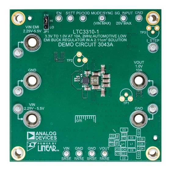
- Page 2 DEMO MANUAL DC3043A BOARD PHOTO Rev. 0...
-
Page 3: Quick Start Procedure
DEMO MANUAL DC3043A QUICK START PROCEDURE Demonstration circuit 3043A is easy to set up and evaluate 6. To change the frequency, remove R4 and install the desired RT resistor in the R6 location. Note, the MODE/ the performance of the LTC3310-1. Refer to Figure 1 for SYNC pin is an output when R6 is installed and the proper measurement equipment setup and follow the pro- MODE/SYNC pin should have high impedance to GND... - Page 4 DEMO MANUAL DC3043A QUICK START PROCEDURE SCOPE 3.3V Figure 1. Test Setup for the DC3043A Demo Board Figure 2. Technique for Measuring Output Ripple and Step Response Rev. 0...
-
Page 5: Circuit Schematic
DEMO MANUAL DC3043A CIRCUIT SCHEMATIC 2.25V TO 5.5V 0.47µF 1µF 1µF 0.47µF 22µF 22µF 0201 0201 PGOOD 249k MODE/SYNC 100nH 100k LTC3310-1 SSTT 47µF 0.033µF ×7 0.1µF AGND 3.3pF PGND dc3043a CS01 330pF L = COILCRAFT, XEL4030-101ME Load Regulation Efficiency and Power Loss vs Load Current (LTC3310S-1, LTC3310-1) 1.10 1.08... - Page 6 DEMO MANUAL DC3043A EMI TEST RESULTS Conducted EMI Performance (CISPR25 Conducted Emission Test with Class 5 Peak Limits) CLASS 5 PEAK LIMIT –10 MEASURED DATA AMBIENT NOISE –20 FREQUENCY (MHz) dc3043a EMI01 DC3043A DEMO BOARD (WITH EMI FILTER INSTALLED) 3.3V INPUT TO 1V OUTPUT AT 8A, f = 2MHz Radiated EMI Performance (CISPR25 Radiated Radiated EMI Performance (CISPR25 Radiated...
-
Page 7: Theory Of Operation
DEMO MANUAL DC3043A THEORY OF OPERATION Introduction to the DC3043A Select an operating switching frequency below f SW(MAX) Typically, it is desired to obtain an inductor current of 30% The DC3043A demonstration circuit features the of the maximum LTC3310-1 operating load, 10A. Use the LTC3310-1, a fixed 1V output, synchronous step-down formulas below to calculate the inductor value to obtain Silent Switcher.”... -
Page 8: Parts List
VISHAY, CRCW04020000Z0ED RES., 15k, 1%, 1/16W, 0402 VISHAY, CRCW040215K0FKED IC, 5V, FIXED 1V OUTPUT 10A SYNCHRONOUS STEP-DOWN ANALOG DEVICES, LTC3310HV-1#PBF SILENT SWITCHER 2, 18-LQFN Additional Demo Board Circuit Components C1, C18 CAP ., 470µF, TANT. POSCAP , 6.3V, 20%, 7343, 10mΩ, TCF... -
Page 9: Schematic Diagram
Devices for its use, nor for any infringements of patents or other rights of third parties that may result from its use. Specifications subject to change without notice. No license is granted by implication or otherwise under any patent or patent rights of Analog Devices. - Page 10 Board until you have read and agreed to the Agreement. Your use of the Evaluation Board shall signify your acceptance of the Agreement. This Agreement is made by and between you (“Customer”) and Analog Devices, Inc. (“ADI”), with its principal place of business at One Technology Way, Norwood, MA 02062, USA. Subject to the terms and conditions of the Agreement, ADI hereby grants to Customer a free, limited, personal, temporary, non-exclusive, non-sublicensable, non-transferable license to use the Evaluation Board FOR EVALUATION PURPOSES ONLY.
Need help?
Do you have a question about the Linear ADI Power LTC3310-1 and is the answer not in the manual?
Questions and answers