Table of Contents
Advertisement
Quick Links
UM11873
PCF85053ATK-ARD evaluation board
Rev. 1.0 — 17 March 2023
Document information
Information
Keywords
Abstract
Content
2
PCF85053ATK, I
C-bus, RTC, CPU, SRAM, Arduino header, EVK
The PCF85053ATK-ARD evaluation board is an expansion board equipped with Arduino headers,
designated for easy test and design of PCF85053ATK IC, real-time clock/calendar with alarm
function, battery switchover and timestamp functionality, controlled through two Fast-mode
2
I
C-buses. The board is fully compatible with MIMXRT1050-EVKB, LPCXpresso55S69 and
MIMXRT685-EVK, including GUI software control. The board can be attached to any device
equipped with Arduino headers.
User manual
Advertisement
Table of Contents

Related Manuals for NXP Semiconductors PCF85053ATK-ARD


Summary of Contents for NXP Semiconductors PCF85053ATK-ARD
- Page 1 C-bus, RTC, CPU, SRAM, Arduino header, EVK Abstract The PCF85053ATK-ARD evaluation board is an expansion board equipped with Arduino headers, designated for easy test and design of PCF85053ATK IC, real-time clock/calendar with alarm function, battery switchover and timestamp functionality, controlled through two Fast-mode C-buses.
- Page 2 UM11873 NXP Semiconductors PCF85053ATK-ARD evaluation board Revision history Date Description v.1.0 20230317 Initial version UM11873 All information provided in this document is subject to legal disclaimers. © 2023 NXP B.V. All rights reserved. User manual Rev. 1.0 — 17 March 2023...
- Page 3 UM11873 NXP Semiconductors PCF85053ATK-ARD evaluation board IMPORTANT NOTICE For engineering development or evaluation purposes only NXP provides the product under the following conditions: This evaluation kit is for use of ENGINEERING DEVELOPMENT OR EVALUATION PURPOSES ONLY. It is provided as a sample IC pre-soldered to a printed-circuit board to make it easier to access inputs, outputs and supply terminals.
-
Page 4: Introduction
PCF85053ATK-ARD evaluation board 1 Introduction This document describes the PCF85053ATK-ARD demo board. The evaluation board is built around the PCF85053ATK IC and works as an expansion board which can be connected through an Arduino header to various Arduino compatible (including original Arduino Uno R3) boards. The board is intended to test and... -
Page 5: Static Handling Requirements
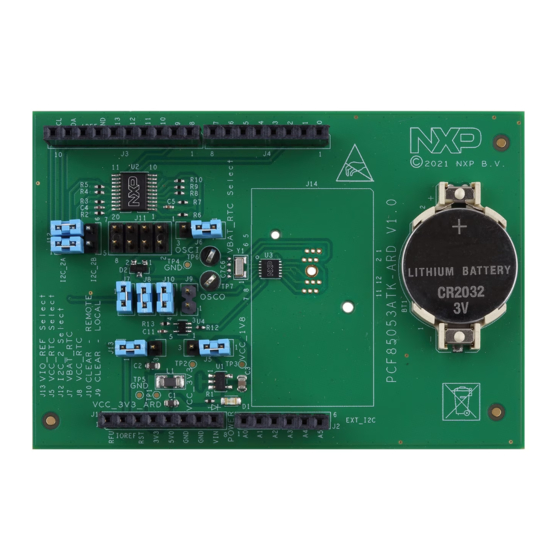
EVK (the motherboard) through the Arduino header, and 1.8 V is generated by the LDO voltage regulator U1. D1 is the power indicator. The PCF85053ATK-ARD board contains the backup battery (BT1), connected to VBAT power pin of the DUT through J6, which allows to supply the VBAT UM11873 All information provided in this document is subject to legal disclaimers. - Page 6 The level shifter U2 assures the voltage translation of the I C-buses, ALRT, and CLKOUT signals. For more details see, the schematic diagram of PCF85053ATK-ARD board (SPF-53085_B1.pdf). Figure 1. PCF85053ATK-ARD evaluation board, top view (up) UM11873 All information provided in this document is subject to legal disclaimers.
-
Page 7: Schematic Diagram
Figure 2. PCF85053ATK-ARD evaluation board,bottom view (down) 4.3 Schematic diagram The schematic diagram of PCF85053ATK-ARD is available at URL: http://www.nxp.com/PCF85053ATK-ARD. 4.4 Arduino headers J1, J2, J3, and J4 are the mated pin headers of Arduino Uno R3 connectors, having the same electrical function and placed on the board, so that the expansion board can be directly inserted into the Arduino headers. -
Page 8: I2C-Buses
UM11873 NXP Semiconductors PCF85053ATK-ARD evaluation board Table 1. The pin chart of Arduino connectors and their usage ...continued Ref Des Arduino label PCF85053ATK-ARD function 3.3V Power supply Not used Power supply return Power supply return Not used Not used Not used... -
Page 9: Jumpers And Test Points
The board contains several jumpers and test points. Table 2 Figure 3 details the jumper locations and their default configurations. Table 3 describes the test points located on the PCF85053ATK-ARD board. Table 2. PCF85053ATK-ARD jumpers Ref Des Label Default Description 1-2: VCC_RTC from VCC_1V8... - Page 10 UM11873 NXP Semiconductors PCF85053ATK-ARD evaluation board Figure 3. PCF85053ATK-ARD jumper locations Table 3. PCF85053ATK-ARD test points Ref Des Test point / jumper label Description VCC_3V3_ARD 3.3 V power rail (Arduino connector) VCC_3V3 3.3 V power rail VCC_1V8 1.8 V power rail Ground...
-
Page 11: Installing And Configuring Software Tools
EVK firmware and GUI host software on PC please download UM11581 - Arduino Shields GUI and firmware installation available at https://www.nxp.com/docs/en/userguide/UM11581.pdf. Once the software is installed, the first step is to select the correct combination EVK – PCF85053ATK-ARD expansion board, and then the board can be controlled from the GUI interface. See... - Page 12 5-6. If using an external power supply (connected to J2), the jumper J1 will be placed in position 1-2. 2. Place jumpers on J12 in 1-2/3-4 position (default). 3. Insert the PCF85053ATK-ARD expansion board on the Arduino connector of the EVK (see Figure 4 Figure 4.
-
Page 13: Using The Pcf85053Atk-Ard With An Lpcxpresso55S69 Development Board
Figure 5. The assembly PCF85053ATK-ARD expansion board / MIMXRT1050-EVK board operation 6.2 Using the PCF85053ATK-ARD with an LPCXpresso55S69 development board Figure 6 shows the required hardware for operation of the PCF85053ATK-ARD and LPCXpresso55S69 EVK board. This configuration consists of: • One LPCXpresso55S69 EVK board •... - Page 14 UM11873 NXP Semiconductors PCF85053ATK-ARD evaluation board Figure 6. PCF85053ATK-ARD expansion board and LPCXpresso55S69 motherboard, before starting UM11873 All information provided in this document is subject to legal disclaimers. © 2023 NXP B.V. All rights reserved. User manual Rev. 1.0 — 17 March 2023...
- Page 15 PCF85053ATK-ARD evaluation board The following steps describe how to assemble, program, and operate the configuration shown in Figure 1. Insert the PCF85053ATK-ARD expansion board to P16 – P19 connectors located on LPCXpresso55S69 development board (see the marked pins of P16 – P19,Figure 2.
- Page 16 UM11873 NXP Semiconductors PCF85053ATK-ARD evaluation board Figure 7. PCF85053ATK-ARD expansion board / LPCXpresso55S69 motherboard operation UM11873 All information provided in this document is subject to legal disclaimers. © 2023 NXP B.V. All rights reserved. User manual Rev. 1.0 — 17 March 2023...
-
Page 17: Using The Pcf85053Atk-Ard With An Mimxrt685-Evk Board
MIMXRT685-EVK board. The datalink between the PC workstation and the EVK is realized through the Target USB (J7). Using the connector J7 and a USB-cable, the assembly MIMXRT685- EVK / PCF85053ATK-ARD can be simultaneously powered and connected to the PC, to be operated from the GUI application. - Page 18 UM11873 NXP Semiconductors PCF85053ATK-ARD evaluation board Figure 8. The assembly PCF85053ATK-ARD expansion board and MIMXRT685-EVK, before starting To configure and operate the setup, follow the below steps: 1. Insert the PCF85053ATK-ARD onto the MIMXRT685-EVK board 2. Configure J12 jumper header as follows: connect pin 3 to pin 6, and pin 4 to pin 5 using the two jumper...
-
Page 19: Using Pcf85053Atk-Ard With Another Device
6.4 Using PCF85053ATK-ARD with another device The PCF85053ATK-ARD expansion board can be operated with any other EVK boards which has an Arduino header. There are two options to connect the board: using other EVK equipped with an Arduino header, and an EVK without Arduino header. -
Page 20: Gui Description
NXP Semiconductors PCF85053ATK-ARD evaluation board 7 GUI description A GUI application is available for the three EVK boards from NXP Semiconductors. The application is common for all above mentioned EVKs (MIMXRT1050-EVKB, LPCXpresso55S69 and MIMXRT685-EVK), produced by NXP Semiconductors. This section describes the GUI application and how the user can control the PCF85053ATK-ARD expansion board from the graphical interface. - Page 21 UM11873 NXP Semiconductors PCF85053ATK-ARD evaluation board Figure 10. Graphical interface at start-up (“Settings” tab activated by default) In the upper area (the blue region), from left to right the following data and commands are displayed: • Date/Time: displays the current date and time stored in the internal registers of the RTC (see below the Date / Time tab description).
- Page 22 UM11873 NXP Semiconductors PCF85053ATK-ARD evaluation board Figure 11. Graphical interface – “Registers” tab activated The next available tab is Registers. Clicking on it, a new interface appears (Figure 11). On the left-hand side of the main window, the user can manually read or write the internal registers of the RTC, by specifying the register address and the number of bytes to be read or written.
- Page 23 UM11873 NXP Semiconductors PCF85053ATK-ARD evaluation board Figure 12. Graphical interface – “Date/Time” tab activated Figure 12 shows the Date / Time tab. In the main window all data regarding the time and the date are present. Notice that under the each parameter the register address and relevant bits within the register are indicated. To change the parameter and write it into the register, click on the parameter’s drop-down menu.
- Page 24 UM11873 NXP Semiconductors PCF85053ATK-ARD evaluation board Figure 13. Graphical interface – “Alarm” tab activated The next tab (see Figure 13) is Alarm. In the same fashion as the previous tab, the RTC registers for the alarm can be written. The CLR button will clear the alarm flag, and the AIE checkbox will enable/disable the Alarm interrupt.
- Page 25 UM11873 NXP Semiconductors PCF85053ATK-ARD evaluation board Figure 14. Graphical interface – “Timestamp” tab activated Figure 14 the Timestamp tab is presented. The timestamp register records any write to the date/time registers. Alongside with the date / time data, a two-byte random number (the R code) is generated and stored by RTC at the timestamp event as unique identifier.
- Page 26 UM11873 NXP Semiconductors PCF85053ATK-ARD evaluation board Figure 15. Graphical interface – “SRAM” tab activated The SRAM tab is shown in Figure 15. From here, the user can write data into the 128-byte SRAM memory of the RTC, or read the current information from the RTC’s SRAM memory. To write data, the user need to specify the address (00h to 7Fh) and enter the desired values to be written into the text field.
- Page 27 UM11873 NXP Semiconductors PCF85053ATK-ARD evaluation board Figure 16. Graphical interface – “CLKOUT/Offset/Battery/Oscillator” tab activated Figure 16 displays the interface of the last tab, Clockout/Offset/Battery/Oscillator. From this tab, the user can manage parameters of the following registers: Oscillator (13h), Status (0Bh), Control (0Ah), CLKOUT Control ((0Ch), and Offset (12h).
-
Page 28: Abbreviations
UM11873 NXP Semiconductors PCF85053ATK-ARD evaluation board 8 Abbreviations Table 6. Abbreviations Acronym Description Device Under Test Electro Static Discharge Evaluation Board Graphical User Interface C bus Inter-Integrated Circuit bus Integrated Circuit Input / Output Light Emitting Diode Personal Computer Real-Time Clock... -
Page 29: References
NXP Semiconductors PCF85053ATK-ARD evaluation board 9 References 1. PCF85053A, Tiny Real-Time Clock/calendar with alarm function, battery switchover, time stamp input, and C-bus Product data sheet; NXP Semiconductors; 2. MIMXRT1050-EVKB Board Hardware User’s Guide https://www.nxp.com/webapp/Download? colCode=MIMXRT1050EVKBHUG User manual; NXP Semiconductors; 3. i.MX RT1050 Crossover Processors Data Sheet for Consumer Products Data sheet;... -
Page 30: Legal Information
NXP Semiconductors. In the event that customer uses the product for design-in and use in In no event shall NXP Semiconductors be liable for any indirect, incidental, automotive applications to automotive specifications and standards, punitive, special or consequential damages (including - without limitation - customer (a) shall use the product without NXP Semiconductors’... -
Page 31: Table Of Contents
I2C-buses ............8 Jumpers and test points ........9 Installing and configuring software tools ..11 Configuring the hardware ........ 11 Using the PCF85053ATK-ARD with an MIMXRT1050-EVK board ........ 11 Using the PCF85053ATK-ARD with an LPCXpresso55S69 development board ...13 Using the PCF85053ATK-ARD with an MIMXRT685-EVK board ........
Need help?
Do you have a question about the PCF85053ATK-ARD and is the answer not in the manual?
Questions and answers