Table of Contents
Advertisement
Quick Links
UM11714
PCF85263ATL-ARD evaluation board
Rev. 1.0 — 17 February 2022
Document information
Information
Content
Keywords
PCF85263ATL, I
Abstract
The PCF85263ATL-ARD evaluation board is a daughterboard equipped with
Arduino port, designated for easy test and design of PCF85263A IC, tiny real-
time clock/calendar with alarm function, battery switch-over and timestamp
input, controlled through Fm I
with IMXRT1050 EVK, LPCXpresso55S69 and i.MX 8M Mini LPDDR4 EVK,
including GUI software control. The board can be attached to any device
equipped with Arduino port.
2
C-bus, RTC, Arduino port, EVK
2
C 2-wire bus. The board is fully compliant
User manual
Advertisement
Table of Contents

Related Manuals for NXP Semiconductors PCF85263ATL-ARD


Summary of Contents for NXP Semiconductors PCF85263ATL-ARD
- Page 1 PCF85263ATL, I C-bus, RTC, Arduino port, EVK Abstract The PCF85263ATL-ARD evaluation board is a daughterboard equipped with Arduino port, designated for easy test and design of PCF85263A IC, tiny real- time clock/calendar with alarm function, battery switch-over and timestamp input, controlled through Fm I C 2-wire bus.
- Page 2 UM11714 NXP Semiconductors PCF85263ATL-ARD evaluation board Revision history Date Description v1.0 20220217 Initial version UM11714 All information provided in this document is subject to legal disclaimers. © NXP B.V. 2022. All rights reserved. User manual Rev. 1.0 — 17 February 2022...
- Page 3 UM11714 NXP Semiconductors PCF85263ATL-ARD evaluation board IMPORTANT NOTICE For engineering development or evaluation purposes only NXP provides the product under the following conditions: This evaluation kit is for use of ENGINEERING DEVELOPMENT OR EVALUATION PURPOSES ONLY. It is provided as a sample IC pre- soldered to a printed-circuit board to make it easier to access inputs, outputs and supply terminals.
-
Page 4: Introduction
The NXP community is at http://community.nxp.com. Getting ready Working with the PCF85263ATL-ARD requires the kit contents, additional hardware, and a Windows PC workstation with installed software. 3.1 Kit contents • Assembled and tested evaluation board in an antistatic bag •... -
Page 5: Static Handling Requirements
• Compliant with i.MX Mini LPDDR4 EVK board, including GUI (Windows 10) Note: For i.MX Mini LPDDR4 EVK Board is necessary to use IMX8MMINI-IARD interposer board between the EVK and PCF85263ATL-ARD daughterboard (see IMX8MMINI-IARD User Manual). 4.2 Kit featured components Figure 1 identifies the main components on the board. - Page 6 The board is powered through the Arduino connector J6 (pin 4 – 3.3V, pin 6, 7 – GND). The power is delivered to the DUT through J37 (located on the PCF85263ATL-ARD board). The role of J37 is to allow the user to perform power-off tests and current measurements.
-
Page 7: Schematic Diagram
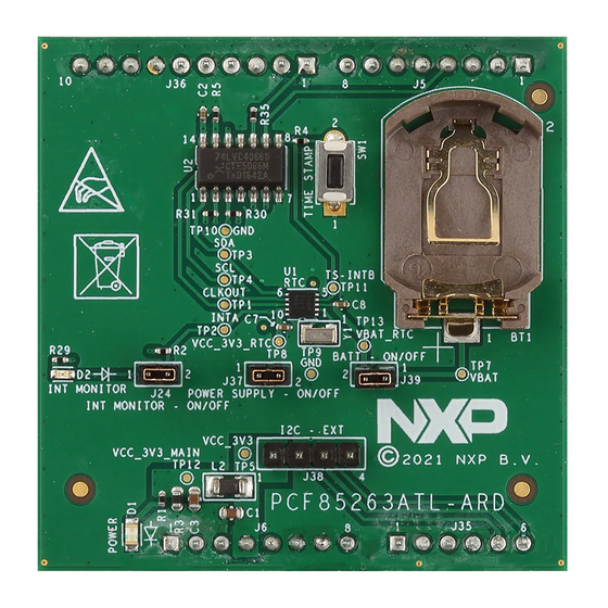
UM11714 NXP Semiconductors PCF85263ATL-ARD evaluation board Figure 1. The PCF85263ATL-ARD board picture, top view (up) and bottom view (down) 4.3 Schematic diagram The schematic diagram of PCF85263ATL-ARD is available at URL: http://www.nxp.com/ PCF85263ATL-ARD. UM11714 All information provided in this document is subject to legal disclaimers. -
Page 8: Arduino Port
UM11714 NXP Semiconductors PCF85263ATL-ARD evaluation board 4.4 Arduino port J5, J6, J35, and J36 are the mated pin headers of Arduino Uno R3 connectors, having the same electrical function and placed on the board, so that the daughterboard can be directly inserted in the Arduino port. The daughterboard uses only four signal lines. -
Page 9: I2C External Connector (J38)
(ground). 4.5 I2C external connector (J38) The I C-bus of the PCF85263A can be directly accessed from external through the connector J38, located on the PCF85263ATL-ARD daughterboard. Table 2 describes the pin chart of J38. Table 2. J38 pin chart J38 pin no. -
Page 10: Installing And Configuring Software Tools
VBAT power rail Installing and configuring software tools PCF85263ATL-ARD evaluation board is designed and built as a daughterboard able to work in conjunction with a motherboard equipped with an Arduino port. The board was built to be fully compatible with the following NXP Evaluation (EVK) boards: •... -
Page 11: Configuring The Hardware
EVK firmware and GUI host software on PC please download EVK_Firmware_And_GUI_Install_Guide_For_Arduino_Boards.pdf instruction file from NXP site (www.nxp.com/). Once the software is installed, the first step is to select the correct combination EVK – PCF85263ATL-ARD daughterboard, and then the board can be controlled from the GUI interface. See Section 6... - Page 12 J1 jumper shall be placed in position 5-6. If using an external power supply (connected to J2), the jumper J1 will be placed in position 1-2. 2. Insert the PCF85263ATL-ARD daughterboard on the Arduino connector of the EVK (see...
-
Page 13: Using The Pcf85263Atl-Ard With An Lpcxpresso55S69 Development Board
UM11714 NXP Semiconductors PCF85263ATL-ARD evaluation board Figure 4. The assembly PCF85263ATL-ARD daughterboard / IMXRT1050 EVK board operation 6.2 Using the PCF85263ATL-ARD with an LPCXpresso55S69 development board Figure 5 shows the required hardware for operation of the PCF85263ATL-ARD and LPCXpresso55S69 EVK board. This configuration consists of: •... - Page 14 The following steps describe how to assemble, program, and operate the configuration shown in Figure 1. Insert the PCF85263ATL-ARD daughterboard to P16 – P19 connectors located on LPCXpresso55S69 development board (see the marked pins of P16 – P19, Figure 2. Connect the development board using port P6 USB port of PC;...
-
Page 15: Mini Lpddr4 Evk Board
6.3 Using the PCF85263ATL-ARD with an i.MX 8M Mini LPDDR4 EVK board When an i.MX 8M Mini LPDDR4 EVK board is used with the PCF85263ATL-ARD board, a third board (IMX8MMINI-IARD interposer board) must be used, especially designed and built as EVK – daughterboard interconnection. The EVK board i.MX 8M Mini LPDDR4 is not equipped with an Arduino port;... - Page 16 NXP Semiconductors PCF85263ATL-ARD evaluation board It is recommended to attach the PCF85263ATL-ARD to the Arduino connectors of the IMX8MMINI-IARD interposer board first, and then the resulting assembly to the i.MX 8M Mini LPDDR4 EVK. This can be done by plugging J1 connector located on the interposer board to J1003 connector on the EVK.
-
Page 17: Using Pcf85263Atl-Ard With Another Device
Arduino port, and an EVK without Arduino port. In the first case, a firmware shall be developed according with PCF85263A specifications, and then simply attach PCF85263ATL-ARD daughterboard to the EVK, to operate the board. In the second case, using the pin chart of Arduino connectors... - Page 18 NXP Semiconductors PCF85263ATL-ARD evaluation board Once installation is complete, assure that one of the mentioned three EVK with attached PCF85263ATL-ARD daughterboard is connected to PC and powered-on. Open NXP_GUI(PCF85063TP,PCF85263ATL,PCF85063A) GUI application. An interface will appear as is shown in Figure The GUI application starts with Settings tab (marked with red arrow).
- Page 19 UM11714 NXP Semiconductors PCF85263ATL-ARD evaluation board the PCF85263A IC for real-time clock, alarm, and timestamps functions when the RTC is in real-time clock mode. A subset of secondary tabs is available in the upper left of the window. Table 5 details the function and the register address for each tab.
- Page 20 UM11714 NXP Semiconductors PCF85263ATL-ARD evaluation board Figure 11. Graphical interface – “Real Time Clock” / “Alarm” tab activated Figure 12. Graphical interface – “Real Time Clock” / “Timestamps” tab activated UM11714 All information provided in this document is subject to legal disclaimers.
- Page 21 UM11714 NXP Semiconductors PCF85263ATL-ARD evaluation board Figure 13. Graphical interface – “Real Time Clock” / “Timestamp Mode” tab activated If from Device Setting section the Stop Watch mode is selected, the second main tab name is switched to Stop Watch. Clicking on Stop Watch tab, a different window...
- Page 22 UM11714 NXP Semiconductors PCF85263ATL-ARD evaluation board Figure 14. Graphical interface – “Stop Watch” / “Time” tab activated Figure 15. Graphical interface – “Stop Watch” / “Alarm” tab activated UM11714 All information provided in this document is subject to legal disclaimers. © NXP B.V. 2022. All rights reserved.
- Page 23 UM11714 NXP Semiconductors PCF85263ATL-ARD evaluation board Figure 16. Graphical interface – “Stop Watch” / “Timestamps” tab activated Figure 17. Graphical interface – “Stop Watch” / “Timestamp mode” tab activated The Configuration tab also contains a subset of secondary tabs, available in the upper left of the window.
- Page 24 UM11714 NXP Semiconductors PCF85263ATL-ARD evaluation board Table 7. The secondary tabs under Configuration main tab ...continued Tab name The picture in: Register address Register function Battery Switch Figure 20 Function Figure 21 Offset Figure 22 Offset register Interrupts Figure 23 29h, 2Ah...
- Page 25 UM11714 NXP Semiconductors PCF85263ATL-ARD evaluation board Figure 19. Graphical interface – “Configuration” / “Pin I/O” tab activated Figure 20. Graphical interface – “Configuration” / “Battery Switch” tab activated UM11714 All information provided in this document is subject to legal disclaimers. © NXP B.V. 2022. All rights reserved.
- Page 26 UM11714 NXP Semiconductors PCF85263ATL-ARD evaluation board Figure 21. Graphical interface – “Configuration” / “Function” tab activated Figure 22. Graphical interface – “Configuration” / “Offset” tab activated UM11714 All information provided in this document is subject to legal disclaimers. © NXP B.V. 2022. All rights reserved.
- Page 27 UM11714 NXP Semiconductors PCF85263ATL-ARD evaluation board Figure 23. Graphical interface – “Configuration” / “Interrupts” tab activated Figure 24. Graphical interface – “Configuration” / “Flags” tab activated UM11714 All information provided in this document is subject to legal disclaimers. © NXP B.V. 2022. All rights reserved.
- Page 28 UM11714 NXP Semiconductors PCF85263ATL-ARD evaluation board Figure 25. Graphical interface – “Configuration” / “Reset/Stop Enable” tab activated The Misc tab contains a subset of two secondary tabs. Table 8 details the function and the register address for the two tabs. For more details about register map, see the datasheet of PCF85263A IC (section Control and function registers).
- Page 29 UM11714 NXP Semiconductors PCF85263ATL-ARD evaluation board Figure 27. Graphical interface – “Misc” / “WatchDog” tab activated UM11714 All information provided in this document is subject to legal disclaimers. © NXP B.V. 2022. All rights reserved. User manual Rev. 1.0 — 17 February 2022...
-
Page 30: Abbreviations
UM11714 NXP Semiconductors PCF85263ATL-ARD evaluation board Abbreviations Table 9. Abbreviations Acronym Description Device Under Test Electro Static Discharge Evaluation Board Graphical User Interface C bus Inter-Integrated Circuit bus Integrated Circuit Input / Output Light Emitting Diode Personal Computer Real-Time Clock Universal Serial Bus UM11714 All information provided in this document is subject to legal disclaimers. -
Page 31: References
1. PCF85263A, Tiny Real-Time Clock/calendar with alarm function, battery switch-over, time stamp input, and I C-bus Product data sheet; NXP Semiconductors; 2. MIMxrt1050 EVK Board Hardware User’s Guide User manual; NXP Semiconductors; 3. i.MX RT1050 Crossover Processors Data Sheet for Consumer Products Data sheet;... -
Page 32: Legal Information
NXP Semiconductors. In the event that customer uses the product for design-in and use in In no event shall NXP Semiconductors be liable for any indirect, incidental, automotive applications to automotive specifications and standards, punitive, special or consequential damages (including - without limitation - customer (a) shall use the product without NXP Semiconductors’... - Page 33 ..............28 Clock main tab ..........19 Tab. 9. Abbreviations ...........30 Figures Fig. 1. The PCF85263ATL-ARD board picture, top Fig. 14. Graphical interface – “Stop Watch” / “Time” view (up) and bottom view (down) ....7 tab activated ............22 Fig. 2.
-
Page 34: Table Of Contents
Using the PCF85263ATL-ARD with an IMXRT1050 EVK board ........11 Using the PCF85263ATL-ARD with an LPCXpresso55S69 development board ...13 Using the PCF85263ATL-ARD with an i.MX 8M Mini LPDDR4 EVK board ......15 Using PCF85263ATL-ARD with another device ...............17 GUI description ..........17 Abbreviations ............
Need help?
Do you have a question about the PCF85263ATL-ARD and is the answer not in the manual?
Questions and answers