Table of Contents
Advertisement
Quick Links
UM11761
PCA9955BTW-ARD evaluation board
Rev. 1.0 — 18 March 2022
Document information
Information
Content
Keywords
PCA9955B, I
Abstract
The "PCA9955BTW-ARD" evaluation board is a daughterboard equipped
with Arduino port, designated for easy test and design of PCA9955B IC, 16-
channel Fm+ I
fully compliant with IMXRT1050 EVK, LPCXpresso55S69 and i.MX 8M Mini
LPDDR4 EVK, including GUI software control. The board can be attached to
any device equipped with Arduino port.
2
C-bus, LED, LED driver, Arduino port, EVK
2
C-bus 57 mA / 20 V constant current LED driver. The board is
User manual
Advertisement
Table of Contents

Related Manuals for NXP Semiconductors PCA9955BTW-ARD


Summary of Contents for NXP Semiconductors PCA9955BTW-ARD
- Page 1 PCA9955B, I C-bus, LED, LED driver, Arduino port, EVK Abstract The “PCA9955BTW-ARD” evaluation board is a daughterboard equipped with Arduino port, designated for easy test and design of PCA9955B IC, 16- channel Fm+ I C-bus 57 mA / 20 V constant current LED driver. The board is fully compliant with IMXRT1050 EVK, LPCXpresso55S69 and i.MX 8M Mini...
- Page 2 UM11761 NXP Semiconductors PCA9955BTW-ARD evaluation board Revision history Date Description v1.0 20220318 Initial version UM11761 All information provided in this document is subject to legal disclaimers. © NXP B.V. 2022. All rights reserved. User manual Rev. 1.0 — 18 March 2022...
- Page 3 UM11761 NXP Semiconductors PCA9955BTW-ARD evaluation board IMPORTANT NOTICE For engineering development or evaluation purposes only NXP provides the product under the following conditions: This evaluation kit is for use of ENGINEERING DEVELOPMENT OR EVALUATION PURPOSES ONLY. It is provided as a sample IC pre- soldered to a printed-circuit board to make it easier to access inputs, outputs and supply terminals.
-
Page 4: Introduction
The PCA9959BTW-ARD board is equipped with a pair of dedicated connectors which allow to interconnect more boards in a chain architecture. The PCA9955BTW-ARD board can be powered in two ways: from the EVK through the Arduino port, or externally through a dedicated power connector, located on the daughterboard. -
Page 5: Kit Contents
• Fully compliant with LPCXpresso55S69 development board, including GUI (Windows • Compliant with i.MX Mini LPDDR4 EVK board, including GUI (Windows 10) Note: For i.MX Mini LPDDR4 EVK Board is necessary to use IMX8MMINI-IARD interposer board between the EVK and PCA9955BTW-ARD daughterboard (see IMX8MMINI-IARD User Manual). UM11761 All information provided in this document is subject to legal disclaimers. -
Page 6: Kit Featured Components
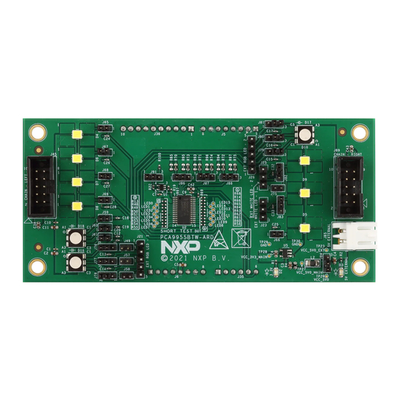
LEDs connected to the driver are placed around the PCA9955B IC. The Arduino port connectors (J5, J6, J35, J36) are located on the bottom side of the board. Figure 1. PCA9955BTW-ARD arduino board: top view (up) and bottom view (down) 4.3 Schematic diagram The schematic diagram of PCA9955BTW-ARD is available at URL: http://www.nxp.com/... - Page 7 IC (U2, pin 2, 3, and 4). For details, see PCA9955B datasheet (NXP Semiconductors). The jumper headers J86, J87 and J88, allow to select only 27 from 125 possible addresses.
- Page 8 5, and 25). Driving low the OE input, enables all sixteen outputs of the LED driver. Driving low the RESET input, sets the internal registers of PCA9959B to their default state. For more details, see PCA9955B datasheet (NXP Semiconductors). The limit current for each output of PCA9955B is set by a resistor connected between REXT (U2, pin 1) and ground.
-
Page 9: Arduino Port
UM11761 NXP Semiconductors PCA9955BTW-ARD evaluation board the corresponding lines of white LEDs D9 and D10 can be redirected with J82 and J83 jumpers to white LED external connectors J23 and J25. 4.5 Arduino port J5, J6, J35, and J36 are the mated pin headers of Arduino Uno R3 connectors, having the same electrical function and placed on the board, so that the daughterboard can be directly inserted in the Arduino port. -
Page 10: Power Distribution
(ground). 4.6 Power distribution The electrical circuit of PCA9955BTW-ARD is supplied from 5 V and 3.3 V power rails. The 5 V power supply can be provided from two sources: from the EVK through the Arduino port, and externally through the power connector J85. The jumper header J8 selects the 5 V source. -
Page 11: Jumpers And Test Points
The board contains 25 jumpers and 22 test points. Table 4 Figure 4 details the jumper locations and their default configurations. Table 5 describes the test points located on the PCA9955BTW-ARD board. Table 4. PCA9955BTW-ARD jumpers Ref Des Default Description 1-2: Imax - REMOTE 2-3: Imax - 20 mA... - Page 12 UM11761 NXP Semiconductors PCA9955BTW-ARD evaluation board Table 4. PCA9955BTW-ARD jumpers ...continued Ref Des Default Description OFF: D7 – OFF (LED D7 disconnected from driver) ON: D8 – ON (LED D8 connected to driver) OFF: D8 – OFF (LED D8 disconnected from driver) 1-2: EXTERNAL (external LED) 2-3: D9 –...
- Page 13 ON – SHORT TEST (D16/RED shorted) OFF (D16/GREEN – normal operation) ON – SHORT TEST (D16/GREEN shorted) OFF (D16/BLUE – normal operation) ON – SHORT TEST (D16/BLUE shorted) Figure 4. PCA9955BTW-ARD Jumper locations Table 5. PCA9955BTW-ARD test points Ref Des Test point / jumper label Description...
-
Page 14: Installing And Configuring Software Tools
Ground Installing and configuring software tools PCA9955BTW-ARD evaluation board is designed and built as a daughterboard able to work in conjunction with a motherboard equipped with an Arduino port. The board was built to be fully compatible with the following NXP Evaluation (EVK) boards: •... - Page 15 J1 jumper shall be placed in position 5-6. If using an external power supply (connected to J2), the jumper J1 will be placed in position 1-2. 2. Insert the PCA9955BTW-ARD daughterboard on the Arduino connector of the EVK (see...
-
Page 16: Using The Pca9955Btw-Ard With An Lpcxpresso55S69 Development Board
UM11761 NXP Semiconductors PCA9955BTW-ARD evaluation board Figure 6. The assembly PCA9955BTW-ARD daughterboard / IMXRT1050 EVK board operation 6.2 Using the PCA9955BTW-ARD with an LPCXpresso55S69 development board Figure 7 shows the required hardware for operation of the PCA9955BTW-ARD and LPCXpresso55S69 EVK board. This configuration consists of: •... - Page 17 The following steps describe how to assemble, program, and operate the configuration shown in Figure 1. Insert the PCA9955BTW-ARD daughterboard to P16 – P19 connectors located on LPCXpresso55S69 development board (see the marked pins of P16 – P19, Figure 2. Connect the development board using port P6 USB port of PC 3.
-
Page 18: Mini Lpddr4 Evk Board
6.3 Using the PCA9955BTW-ARD with an i.MX 8M Mini LPDDR4 EVK board When an i.MX 8M Mini LPDDR4 EVK board is used with the PCA9955BTW-ARD board, a third board (IMX8MMINI-IARD interposer board) must be used, especially designed and built as an EVK/daughterboard interconnection. The EVK board i.MX 8M Mini LPDDR4 is not equipped with an Arduino port;... - Page 19 PCA9955BTW-ARD evaluation board • A PC with Windows 10 operating system It is recommended to attach the PCA9955BTW-ARD to the Arduino connectors of the IMX8MMINI-IARD interposer board first, and then the resulting assembly to the i.MX 8M Mini LPDDR4 EVK. This can be done by plugging J1 connector located on the interposer board to J1003 connector on the EVK.
-
Page 20: Using Pca9955Btw-Ard With Another Device
EVK. Assure for correct electrical connections and avoid data conflicts on the signal lines, to prevent IC damage. GUI description A GUI application is available for the three EVK boards from NXP Semiconductors. The application is common for all three EVKs described in Section This section describes the GUI application and how the user can control the PCA9955BTW-ARD daughterboard from the graphical interface. -
Page 21: Settings Tab
In the right side of the blue region are located two read-only flags mapped in “MODE2” register (#01h). The FAULT flag indicates that the PCA9955BTW-ARD’s internal controller has detected an LED output error (no load, short). The OVERTEMP flag indicates that the PCA9955B die temperature exceeds its specified limit (see the PCA9955B datasheet, Section 7.3.15 “LED error detection”... - Page 22 UM11761 NXP Semiconductors PCA9955BTW-ARD evaluation board • REXT Settings selects the maximum current delivered by the LED: 20 mA (default value) or 50 mA. • OE controls the OE input of the DUT. • I2C Frequency displays the I2C-bus clock frequency. The drop-down box allows the selection of three values: 100 kHz (default value), 400 kHz and 1 MHz.
-
Page 23: Global
UM11761 NXP Semiconductors PCA9955BTW-ARD evaluation board 7.2 Global Figure 12. Graphical interface – Global / Brightness tab activated The Global contains two secondary tabs. The default secondary tab is Brightness (see the red left arrows in Figure 12). The two secondary tabs sets the “PWMAL” (44h) and “IREFALL”... -
Page 24: Channels Tab
UM11761 NXP Semiconductors PCA9955BTW-ARD evaluation board Figure 13. Graphical interface – Global / Gain tab activated 7.3 Channels tab Figure 14. Graphical interface – Channels / Brightness tab activated The Channels contains eight secondary tabs. The default secondary tab from Channels is Brightness (see the red left arrows in Figure 14). - Page 25 UM11761 NXP Semiconductors PCA9955BTW-ARD evaluation board Table 8. Secondary tabs under Channels tab ...continued Secondary tab Picture in Register name Register HEX Remarks Output Figure 16 LEDOUT0 to LEDOUT3 #02h – #05h Read / Write / Write All GRADMODE_SEL0 Gradation Figure 17 #38h –...
- Page 26 UM11761 NXP Semiconductors PCA9955BTW-ARD evaluation board Figure 16. Graphical interface – Channels / Output tab activated Figure 17. Graphical interface – Channels / Gradation tab activated UM11761 All information provided in this document is subject to legal disclaimers. © NXP B.V. 2022. All rights reserved.
- Page 27 UM11761 NXP Semiconductors PCA9955BTW-ARD evaluation board Figure 18. Graphical interface – Channels / Errors tab activated Figure 19. Graphical interface – Channels / Sub I2C Address tab activated UM11761 All information provided in this document is subject to legal disclaimers. © NXP B.V. 2022. All rights reserved.
-
Page 28: Groups Tab
PCA9955B IC. In Section 8 a set of instructions are provided, to help the user for quick check of the PCA9955BTW-ARD board and understanding how to write the registers of the PCA9955B IC. UM11761 All information provided in this document is subject to legal disclaimers. - Page 29 UM11761 NXP Semiconductors PCA9955BTW-ARD evaluation board Figure 21. Graphical interface – Channels / Blink tab activated Figure 22. Graphical interface – Groups / Gain tab activated UM11761 All information provided in this document is subject to legal disclaimers. © NXP B.V. 2022. All rights reserved.
- Page 30 UM11761 NXP Semiconductors PCA9955BTW-ARD evaluation board Figure 23. Graphical interface – Channels / Ramping tab activated Figure 24. Graphical interface – Channels / Step time tab activated UM11761 All information provided in this document is subject to legal disclaimers. © NXP B.V. 2022. All rights reserved.
- Page 31 UM11761 NXP Semiconductors PCA9955BTW-ARD evaluation board Figure 25. Graphical interface – Channels / Hold tab activated Figure 26. Graphical interface – Channels / All Call I2C tab activated UM11761 All information provided in this document is subject to legal disclaimers. © NXP B.V. 2022. All rights reserved.
-
Page 32: Operation Example
Figure 28. Graphical interface – Channels / Define tab activated Operation example This section details the necessary steps to operate the PCA9955BTW-ARD daughterboard with one of three EVKs from the GUI. This will help the user for a quick test of the board, and a guidance to understand the register functionality. After the... -
Page 33: Abbreviations
UM11761 NXP Semiconductors PCA9955BTW-ARD evaluation board 3. From Select COM Port list, select the correct COM (if more than one is available). 4. From Select Board list, select PCA9955B. 5. Click Connect. When the connection is established, all on-board LEDs are turned on. - Page 34 UM11761 NXP Semiconductors PCA9955BTW-ARD evaluation board Table 10. Abbreviations ...continued Acronym Description C bus Inter-Integrated Circuit bus Integrated Circuit Input / Output Light Emitting Diode Personal Computer Universal Serial Bus UM11761 All information provided in this document is subject to legal disclaimers.
-
Page 35: References
PCA9955BTW-ARD evaluation board 10 References 1. PCA9955B – 16-channel Fm+ I2C-bus 57 mA/20 V constant current LED driver Product data sheet; NXP Semiconductors; 2. MIMxrt1050 EVK Board Hardware User’s Guide User manual; NXP Semiconductors; 3. i.MX RT1050 Crossover Processors Data Sheet for Consumer Products Data sheet;... -
Page 36: Legal Information
NXP Semiconductors. In the event that customer uses the product for design-in and use in In no event shall NXP Semiconductors be liable for any indirect, incidental, automotive applications to automotive specifications and standards, punitive, special or consequential damages (including - without limitation - customer (a) shall use the product without NXP Semiconductors’... - Page 37 Graphical interface – Channels / Gain tab view (up) and bottom view (down) ....6 activated ............25 Fig. 2. PCA9955BTW-ARD block diagram ....7 Fig. 16. Graphical interface – Channels / Output tab Fig. 3. PCA9955BTW-ARD chain configuration ..11 activated ............
-
Page 38: Table Of Contents
Using the PCA9955BTW-ARD with an IMXRT1050 EVK board ........14 Using the PCA9955BTW-ARD with an LPCXpresso55S69 development board ...16 Using the PCA9955BTW-ARD with an i.MX 8M Mini LPDDR4 EVK board ......18 Using PCA9955BTW-ARD with another device ...............20 GUI description ..........20 Settings tab ............21...
Need help?
Do you have a question about the PCA9955BTW-ARD and is the answer not in the manual?
Questions and answers