Table of Contents
Advertisement
Quick Links
FEATURES
Dual-channel, 1024-position resolution
25 kΩ, 250 kΩ nominal resistance
Low temperature coefficient: 35 ppm/°C
Nonvolatile memory stores wiper settings
Permanent memory write protection
Wiper setting readback
Resistance tolerance stored in EEMEM
Predefined linear increment/decrement instructions
Predefined ±6 dB/step log taper increment/decrement
instructions
SPI® compatible serial interface
3 V to 5 V single supply or ±2.5 V dual supply
26 bytes extra nonvolatile memory for user-defined
information
100-year typical data retention, T
Power-on refreshed with EEMEM settings
APPLICATIONS
DWDM laser diode driver, optical supervisory systems
Mechanical potentiometer replacement
Instrumentation: gain, offset adjustment
Programmable voltage to current conversion
Programmable filters, delays, time constants
Programmable power supply
Low resolution DAC replacement
Sensor calibration
GENERAL DESCRIPTION
The AD5235 is a dual-channel, nonvolatile memory,
2
controlled potentiometer
with 1024-step resolution. The device
performs the same electronic adjustment function as a
mechanical potentiometer with enhanced resolution, solid state
reliability, and superior low temperature coefficient perform-
ance. The AD5235's versatile programming via an SPI
compatible serial interface allows 16 modes of operation and
adjustment including scratchpad programming, memory
storing and restoring, increment/decrement, ±6 dB/step log
taper adjustment, wiper setting readback, and extra EEMEM for
user-defined information such as memory data for other
components, look-up table, or system identification
information.
Rev. B
Information furnished by Analog Devices is believed to be accurate and reliable.
However, no responsibility is assumed by Analog Devices for its use, nor for any
infringements of patents or other rights of third parties that may result from its use.
Specifications subject to change without notice. No license is granted by implication
or otherwise under any patent or patent rights of Analog Devices. Trademarks and
registered trademarks are the property of their respective owners.
= 55°C
A
1
digitally
Nonvolatile Memory, Dual
1024-Position Digital Potentiometer
FUNCTIONAL BLOCK DIAGRAM
ADDR
CS
DECODE
CLK
SERIAL
SDI
INTERFACE
SDO
POWER-ON
PR
RESET
WP
EEMEM
CONTROL
RDY
In the scratchpad programming mode, a specific setting can be
programmed directly to the RDAC
resistance between Terminals W–A and W–B. This setting can
be stored into the EEMEM and is restored automatically to the
RDAC register during system power-on.
The EEMEM content can be restored dynamically or through
external PR strobing, and a WP function protects EEMEM
contents. To simplify the programming, the independent or
simultaneous linear-step increment or decrement commands
can be used to move the RDAC wiper up or down, one step at a
time. For logarithmic ±6 dB changes in wiper setting, the left or
right bit shift command can be used to double or half the
RDAC wiper setting.
AD5235 patterned resistance tolerance is stored in the EEMEM.
The actual end-to-end resistance can, therefore, be known by
the host processor in readback mode. The host can execute the
appropriate resistance step through a software routine that
simplifies open-loop applications as well as precision calibration
and tolerance matching applications.
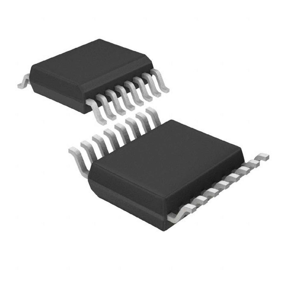
The AD5235 is available in a thin TSSOP-16 package. The part
is guaranteed to operate over the extended industrial tempera-
ture range of −40°C to +85°C.
1
The terms nonvolatile memory and EEMEM are used interchangeably.
2
The terms digital potentiometer and RDAC are used interchangeably.
3
R
tolerance.
AB
One Technology Way, P.O. Box 9106, Norwood, MA 02062-9106, U.S.A.
Tel: 781.329.4700
Fax: 781.326.8703
AD5235
RDAC1
REGISTER
RDAC1
EEMEM1
RDAC2
REGISTER
RDAC2
EEMEM2
26 BYTES
3
RTOL
USER EEMEM
Figure 1.
2
register, which sets the
www.analog.com
© 2004 Analog Devices, Inc. All rights reserved.
AD5235
V
DD
A1
W1
B1
A2
W2
B2
V
SS
GND
Advertisement
Table of Contents

Related Manuals for Analog Devices AD5235


Summary of Contents for Analog Devices AD5235
-
Page 1: Edits To Features, General Description, And Block Diagram
Information furnished by Analog Devices is believed to be accurate and reliable. However, no responsibility is assumed by Analog Devices for its use, nor for any infringements of patents or other rights of third parties that may result from its use. -
Page 2: Table Of Contents
AD5235 TABLE OF CONTENTS Specifications..................3 AD5235EVAL Evaluation Kit ........... 21 Electrical Characteristics—25 kΩ, 250 kΩ Versions....3 Applications..................22 Interface Timing Characteristics—25 kΩ, 250 kΩ Versions... 5 Bipolar Operation from Dual Supplies........22 Timing Diagrams................6 Gain Control Compensation ............ 22 Absolute Maximum Ratings............ -
Page 3: Specifications
AD5235 SPECIFICATIONS ELECTRICAL CHARACTERISTICS—25 KΩ, 250 KΩ VERSIONS = 3 V to 5.5 V, V = 0 V, V = 0 V, −40°C < T < +85°C, unless otherwise noted. The part can be operated at 2.7 V single supply, except from 0°C to −40°C, where a minimum of 3 V is needed. - Page 4 AD5235 Parameter Symbol Conditions Unit EEMEM Store Mode Current (store) or V = GND, ≈ 0 = GND, I (store) = +2.5 V, V = −2.5 V −35 EEMEM Restore Mode Current (restore) or V = GND, ≈ 0 = GND, I (restore) = +2.5 V, V...
-
Page 5: Interface Timing Characteristics-25 Kω, 250 Kω Versions
AD5235 INTERFACE TIMING AND EEMEM RELIABILITY CHARACTERISTICS—25 KΩ, 250 KΩ VERSIONS Guaranteed by design and not subject to production test. See the Timing Diagrams section for the location of measured values. All input control voltages are specified with t = 2.5 ns (10% to 90% of 3 V) and timed from a voltage level of 1.5 V. -
Page 6: Timing Diagrams
AD5235 TIMING DIAGRAMS CPHA = 1 CPOL = 1 HIGH HIGH OR LOW OR LOW B23–MSB B0–LSB B24* B23–MSB B0–LSB *NOTE: EXTRA BIT THAT IS NOT DEFINED, BUT NORMALLY LSB OF CHARACTER PREVIOUSLY TRANSMITTED. THE CPOL = 1 MICROCONTROLLER COMMAND ALIGNS THE INCOMING DATA TO THE POSITIVE EDGE OF THE CLOCK. -
Page 7: Absolute Maximum Ratings
AD5235 ABSOLUTE MAXIMUM RATINGS = 25°C, unless otherwise noted. Table 3. Stresses above those listed under Absolute Maximum Ratings Parameter Rating may cause permanent damage to the device. This is a stress to GND –0.3 V, +7 V rating only and functional operation of the device at these or to GND +0.3 V, −7 V... -
Page 8: Pin Configuration And Function Descriptions
AD5235 PIN CONFIGURATION AND FUNCTION DESCRIPTIONS AD5235BRU TOP VIEW (Not to Scale) Figure 4. Pin Configuration Table 4. Pin Function Descriptions Pin No. Mnemonic Description Serial Input Register Clock. Shifts in one bit at a time on positive clock edges. -
Page 9: Typical Performance Characteristics
AD5235 TYPICAL PERFORMANCE CHARACTERISTICS +25°C +25°C –40°C –40°C +85°C +85°C –0.2 –0.2 –0.4 –0.4 –0.6 –0.6 –0.8 –0.8 –1.0 1000 1000 DIGITAL CODE DIGITAL CODE Figure 5. INL vs. Code, T = −40°C, +25°C, +85°C Overlay, R = 25 kΩ... - Page 10 AD5235 0.28 = 3V = ±2.5V = 0V = 1V rms 0.24 = 25°C 0.20 = 250kΩ 0.16 0.12 25kΩ 0.08 0.04 0.00 1000 1200 0.01k 0.1k 100k CODE (Decimal) FREQUENCY (Hz) Figure 11. Wiper On Resistance vs. Code Figure 14. Total Harmonic Distortion vs. Frequency = 25kΩ...
- Page 11 AD5235 2.64 CODE 0x200 = 5V 2.62 CODE = 0x200 TO 0x1FF –10 0x100 2.60 0x080 2.58 –20 0x040 2.56 0x020 2.54 –30 0x010 2.52 2.50 –40 0x008 2.48 0x004 2.46 –50 0x002 2.44 0x001 –60 2.42 100k FREQUENCY (Hz) TIME (µS)
-
Page 12: Test Circuits
AD5235 = OPEN 5V/DIV = 25°C 5V/DIV = 25kΩ 5V/DIV = 250kΩ 2mA/DIV 4ms/DIV 0.01 * SUPPLY CURRENT RETURNS TO MINIMUM POWER 1024 CONSUMPTION, IF INSTRUCTION 0 (NOP) IS EXECUTED IIMMEDIATELY AFTER INSTRUCTION 1 (READ EEMEM). CODE (Decimal) Figure 23. I vs. - Page 13 AD5235 +15V RDAC1 RDAC2 OP42 OFFSET 2.5V –15V Figure 31. Gain vs. Frequency = 20 LOG [V NC = NO CONNECT Figure 34. Analog Crosstalk 0.1V CODE = 0x00 200µA 0.1V – TO OUTPUT (MIN) TO V A = NC...
-
Page 14: Theory Of Operation
AD5235 THEORY OF OPERATION SCRATCHPAD AND EEMEM PROGRAMMING The AD5235 digital potentiometer is designed to operate as a true variable resistor. The resistor wiper position is determined The scratchpad RDAC register directly controls the position of by the RDAC register contents. The RDAC register acts as a the digital potentiometer wiper. -
Page 15: Eemem Protection
24-bit or 48-bit word, but it cannot work properly chip-select CS is in logic high. ESD protection of the digital with a 23-bit or 25-bit word. In addition, AD5235 has a subtle inputs is shown in Figure 37 and Figure 38. -
Page 16: Terminal Voltage Operating Range
0.1µF Figure 40. Maximum Terminal Voltages Set by V and V The ground pin of the AD5235 device is primarily used as a digital ground reference. To minimize the digital ground Figure 41. Power Supply Bypassing bounce, the AD5235 ground terminal should be joined remotely to the common ground (see Figure 41). - Page 17 AD5235 In Table 6, command bits are C0 to C3, address bits are A0 to A3, data bits D0 to D9 are applicable to RDAC, and D0 to D15 are applicable to EEMEM. Table 6. 24-Bit Serial Data-Word Command Byte 0...
-
Page 18: Advanced Control Modes
Even numbers of bits are ideal. The graph in Figure 42 shows plots of Log_Error [20 × log Four programming instructions produce logarithmic taper (error/code)] for the AD5235. For example, Code 3 Log_Error = increment and decrement of the wiper position control by 20 × log (0.5/3) = −15.56 dB, which is the worst case. -
Page 19: Rdac Structure
AD5235 Using CS to Re-Execute a Previous Command calculated as follows: Another subtle feature of the AD5235 is that a subsequent CS MSB: 1 = Positive strobe, without clock and data, repeats a previous command. Next 7 LSB: 001 1100 = 28 −8... -
Page 20: Programming The Variable Resistor
(0) is 50 Ω because of the wiper resistance, and Like the mechanical potentiometer that the RDAC replaces, the it is independent of the nominal resistance. The second AD5235 part is totally symmetrical. The resistance between connection is the first tap point where R (1) becomes 24.4 Ω + Wiper W and Terminal A also produces a digitally controlled 50 Ω... -
Page 21: Programming Examples
AD5235 Because AD5235 can also be supplied by dual supplies, the Table 16. Restoring the EEMEM Values to RDAC Registers general equation defining the output voltage at V with respect Action to ground for any given input voltages applied to Terminals A... -
Page 22: Applications
BIPOLAR OPERATION FROM DUAL SUPPLIES the performance when R2 is set at low values. On the other The AD5235 can be operated from dual supplies ±2.5 V, which hand, it avoids the ringing or oscillation at the worst case. For... -
Page 23: Bipolar Programmable Gain Amplifier
OP2177 –2.5V V– +2.5V +2.5V –2.5V TRIM AD8552 ADR421 –kVi U1 = U2 = AD5235 V– –2.5V U1 = MIDSCALE AD5235 OP2177 V– Figure 50. 10-Bit Bipolar DAC PROGRAMMABLE VOLTAGE SOURCE WITH BOOSTED OUTPUT Figure 49. Bipolar Programmable Gain Amplifier... -
Page 24: Programmable Current Source
Second, the voltage compliance at V antialiasing filter to band limit the sampling signal. The dual- channel AD5235 can, therefore, be used to construct a second- is limited to 2.5 V or equivalently a 125 Ω load. Should higher order Sallen-Key low-pass filter, as shown in Figure 54. -
Page 25: Programmable Oscillator
2.2nF 25kΩ +2.5V OPTICAL TRANSMITTER CALIBRATION WITH ADN2841 OP1177 The AD5235, together with the multirate 2.7 Gbps laser diode V– – driver ADN2841, forms an optical supervisory system in which 2.1kΩ –2.5V the dual digital potentiometers can be used to set the laser average optical power and extinction ratio (Figure 56). -
Page 26: Resistance Scaling
RESISTANCE SCALING Users should also be aware of the need for tolerance matching The AD5235 offers 25 kΩ or 250 kΩ nominal resistance. For as well as for temperature coefficient matching of the users who need lower resistance but must still maintain the components. -
Page 27: Rdac Circuit Simulation Model
.PARAM D = 1024, RDAC = 25E3 loads dominate the ac characteristics of the RDACs. Configured as a potentiometer divider, the −3 dB bandwidth of the AD5235 .SUBCKT DPOT (A, W, B) (25 kΩ resistor) measures 125 kHz at half-scale. Figure 14... -
Page 28: Outline Dimensions
Line 1 contains the model number. Line 2 contains the ADI logo followed by the end-to-end resistance value. Line 3 contains the date code, YYWW. Z = Pb-free part. © 2004 Analog Devices, Inc. All rights reserved. Trademarks and registered trademarks are the property of their respective owners.
Need help?
Do you have a question about the AD5235 and is the answer not in the manual?
Questions and answers