
Related Manuals for Intersil ISL70321SEHEV Z Series


Summary of Contents for Intersil ISL70321SEHEV Z Series
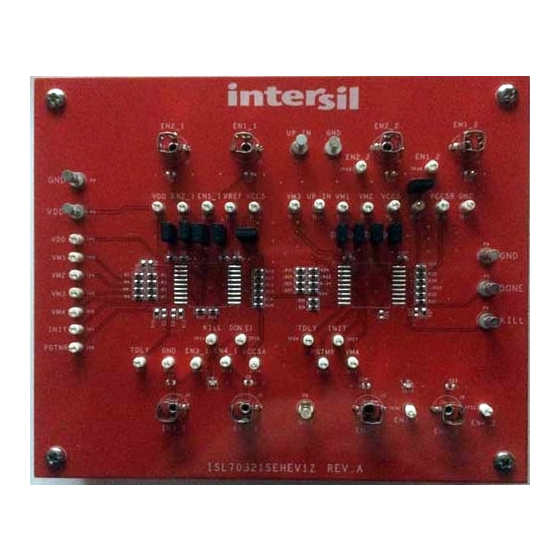
- Page 1 ISL70321SEHEVxZ User’s Manual: Evaluation Board High Reliability Rev 0.00 Sep 2017...
-
Page 2: Specifications
• Jumper enabled for stand alone or POL evaluation • Convenient power connection • Done indicator • Easy interconnectivity with other Intersil boards Specifications This board has been configured for the following default operating conditions: • ISL70321SEHEV1Z for four sequenced outputs •... - Page 3 ISL70321SEHEVxZ 1. Overview INIT INIT VCC5 VCC5 4xEN 8xEN KILL KILL 4xVMIN 8xVMIN DONE DONE ISL70321SEHEV1Z (FOUR OUTPUTS) ISL70321SEHEV2Z (EIGHT OUTPUTS) Figure 1. Block Diagrams UG122 Rev.0.00 Page 3 of 15 Sep 18, 2017...
-
Page 4: Functional Description
VMx inputs so that the sequencing operation can be demonstrated. Using a combination of jumper settings, the ISL70321SEHEV1Z can be used to address the enable inputs of multiple Intersil POL or LDO evaluation boards using the ENx outputs to create a sequenced on and off multi-voltage rail power supply block. -
Page 5: Pcb Layout Guidelines
ISL70321SEHEVxZ 3. PCB Layout Guidelines PCB Layout Guidelines The ISL70321SEH PCB layout requires no special treatment other than the good design practice of placing the VDD, VCC5, and VREF caps close to the IC body. ISL70321SEHEV1Z Evaluation Board POPULATED FOR ISL70321SEHEV1Z LEADER FOLLOWER POPULATED FOR ISL70321SEHEV2Z... - Page 6 ISL70321SEHEVxZ 3. PCB Layout Guidelines SIGNAL UP WITH 2V ISL70003A ENABLE INIT ISL70002 VCC5 4xEN ENABLE KILL 4xVMIN DONE ISL70001A 3.3V ENABLE 1.0V Figure 3. Block Diagram Showing ISL70321SEHEV1Z Enabling Three ISL7000X Regulator Evaluation Boards (See Figures 12, 13) UG122 Rev.0.00 Page 6 of 15 Sep 18, 2017...
- Page 7 ISL70321SEHEVxZ Circuit Schematics LEADER LEADER EN4_1 UNNAMED_1_JUMPER2_I690_IN2 EN3_1 UNNAMED_1_JUMPER2_I689_IN2 VCC5A EN2_1 UNNAMED_1_JUMPER2_I688_IN2 VCC5 EN1_1 UNNAMED_1_JUMPER2_I677_IN2 TP19 TP18 0.47UF TP16 0.22UF UP_IN EN1_1 UNNAMED_1_ISL70321SEH_I543_PIN1 VCC5 UNNAMED_1_ISL70321SEH_I543_PIN17 VREF TP17 6.81K UNNAMED_1_ISL70321SEH_I543_PIN3 UNNAMED_1_ISL70321SEH_I543_PIN4 TP15 UNNAMED_1_ISL70321SEH_I543_PIN5 EN2_1 UNNAMED_1_ISL70321SEH_I543_PIN6 UNNAMED_1_ISL70321SEH_I543_PIN7 INIT DONE DONE1 UNNAMED_1_ISL70321SEH_I543_PIN8 KILL PGTMR KILL TP12...
- Page 8 FOLLOWER FOLLOWER EN4_2 UNNAMED_2_JUMPER2_I92_IN2 EN3_2 UNNAMED_2_JUMPER2_I93_IN2 VCC5B JP10 EN2_2 UNNAMED_2_JUMPER2_I94_IN2 TP35 EN1_2 UNNAMED_2_JUMPER2_I95_IN2 TP37 0.47UF TP36 UP_IN 0.22UF UNNAMED_2_ISL70321SEH_I31_PIN18 TP21 VCC5 TP34 TP22 UNNAMED_2_ISL70321SEH_I31_PIN17 VREF TP23 UNNAMED_2_ISL70321SEH_I31_PIN3 EN1_2 TP24 UNNAMED_2_ISL70321SEH_I31_PIN4 TP25 UNNAMED_2_ISL70321SEH_I31_PIN5 TP26 TP33 UNNAMED_2_ISL70321SEH_I31_PIN6 DONE1 TP27 INIT DONE EN2_2 UNNAMED_2_ISL70321SEH_I31_PIN8 PGTMR KILL...
-
Page 9: Bill Of Materials
3. PCB Layout Guidelines Bill of Materials Reference Manufacturer Item Qty Designator Value Rating Footprint Manufacturer Part Number U1, U2* 18 ld Flat Pack Intersil ISL70321/PROTO 0Ω 1/10W 0603 GENERIC GENERIC R18, R28, R37 1/10W 0603 GENERIC GENERIC C2, C4, C10, C21 0.47µF... - Page 10 ISL70321SEHEVxZ 3. PCB Layout Guidelines Board Layout - Two Layers Figure 6. Top Layer (Silkscreen with Top Layer) UG122 Rev.0.00 Page 10 of 15 Sep 18, 2017...
- Page 11 ISL70321SEHEVxZ 3. PCB Layout Guidelines Figure 7. PCB – Bottom Layer (Viewed from Top) UG122 Rev.0.00 Page 11 of 15 Sep 18, 2017...
-
Page 12: Typical Performance Curves
ISL70321SEHEVxZ 3. PCB Layout Guidelines Typical Performance Curves Unless noted: V = 12V, T = +25°C 2V/DIV 2V/DIV 1ms/DIV 2ms/DIV Figure 8. Off and On EN1 - EN4 Sequencing Figure 9. Up to EN1 through EN4, RTDLY = 10kΩ = 2ms 2V/DIV 2V/DIV 5µs/DIV... - Page 13 ISL70321SEHEVxZ 3. PCB Layout Guidelines Unless noted: V = 12V, T = +25°C (Continued) POL1 VOUT 1V/DIV 5ms/DIV UP/INIT UP/INIT POL2 VOUT POL1 VOUT POL3 VOUT POL2 VOUT 1V/DIV POL3 VOUT 2ms/DIV Figure 12. Sequencing On Three POLs, Figure 13. Sequencing Off Three POLs, RTDLY = 2ms RTDLY = 2ms EN1 of 2nd ISL70321...
-
Page 14: Revision History
All trademarks and registered trademarks are the property of their respective owners. Intersil Corporation reserves the right to make changes in circuit design, software and/or specifications at any time without notice. Accordingly, the reader is cautioned to verify that the document is current before proceeding. - Page 15 ISL70321SEHEVxZ UG122...
Need help?
Do you have a question about the ISL70321SEHEV Z Series and is the answer not in the manual?
Questions and answers