
Related Manuals for NXP Semiconductors i.MX8 QM


Summary of Contents for NXP Semiconductors i.MX8 QM
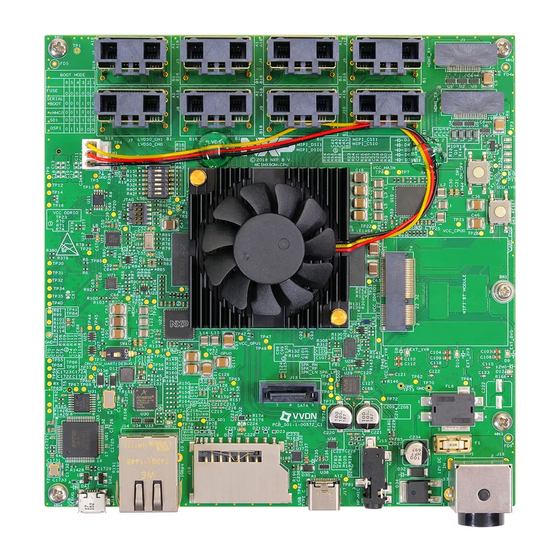
- Page 1 NXP Semiconductors Document identifier: IMX8HWDG User's Guide Rev. 2.4p, 06/2021 i.MX8 QM / i.MX8 QXP Hardware Developer’s Guide...
-
Page 2: Table Of Contents
Chapter 3 i.MX8 layout/routing recommendations..........19 Chapter 4 Thermal considerations...............75 Chapter 5 Avoiding board bring-up problems............81 Chapter 6 Using BSDL for board-level testing............. 86 Chapter 7 Revision history...................87 i.MX8 QM / i.MX8 QXP Hardware Developer’s Guide, Rev. 2.4p, 06/2021 User's Guide 2 / 89... -
Page 3: Chapter 1 Overview
This guide is released along with relevant device-specific hardware documentation such as datasheets, reference manuals, and application notes available at nxp.com. 1.1 Devices supported This Hardware Developer’s Guide currently supports the i.MX8 QM (29 x 29 mm package) and i.MX8 QXP (21 x 21 and 17 x 17 mm packages) processors. 1.2 Essential reference This guide is intended as a companion to the i.MX 8 series chip reference manuals and data sheets. - Page 4 In this guide, notations for all logical, bit-wise, arithmetic, comparison, and assignment operations follow C Language conventions. 1.6 Acronyms and abbreviations Table 1 defines the acronyms and abbreviations used in this document. i.MX8 QM / i.MX8 QXP Hardware Developer’s Guide, Rev. 2.4p, 06/2021 User's Guide 4 / 89...
- Page 5 Inter-integrated Circuit interface IBIS Input output Buffer Information Specification IOMUX i.MX8 chip-level I/O Multiplexing JTAG Joint Test Action Group Table continues on the next page... i.MX8 QM / i.MX8 QXP Hardware Developer’s Guide, Rev. 2.4p, 06/2021 User's Guide 5 / 89...
- Page 6 Plated Through Hole PCB (no microvias) RGMII Reduced Gigabit Media Independent Interface (Ethernet) RMII Reduced Media Independent Interface (Ethernet) Read-Only Memory Upstream Facing Port (USB Type-C) i.MX8 QM / i.MX8 QXP Hardware Developer’s Guide, Rev. 2.4p, 06/2021 User's Guide 6 / 89...
-
Page 7: Chapter 2 I.mx8 Qm And Qxp Design Checklist
QM and QXP design checklist This document provides a design checklist for the i.MX8 QM (29 x 29 mm package) and i.MX8 QXP (21 x 21 mm package) processors. The design checklist tables contain recommendations for optimal design. Where appropriate, the checklist tables also provide an explanation of the recommendation so that users have a greater understanding of why certain techniques are recommended. - Page 8 JTAG_TDO. that the floating condition is actively eliminated if an external pull resistor is not present. Table continues on the next page... i.MX8 QM / i.MX8 QXP Hardware Developer’s Guide, Rev. 2.4p, 06/2021 User's Guide 8 / 89...
- Page 9 (desired trace length < 50 mils). The HDMI RX LDO • VDD_HDMI_TX0_LDO_1P0_CAP outputs should only be connected to the caps, while the Table continues on the next page... i.MX8 QM / i.MX8 QXP Hardware Developer’s Guide, Rev. 2.4p, 06/2021 User's Guide 9 / 89...
- Page 10 µF cap and two 0.22 µF caps. trace length < 50 mils). This LDO output should only drive VDD_USB_OTG1_1P0. See the i.MX8QM LPDDR4 MEK layout for the recommended capacitor placement. i.MX8 QM / i.MX8 QXP Hardware Developer’s Guide, Rev. 2.4p, 06/2021 User's Guide 10 / 89...
- Page 11 Place a 0.22 µF cap under the BGA package. VDD_ANAn_1P8 VDD_SCU_1P8_n 2.2 µF caps should be placed under VDD_SCU_ANA_1P8 the BGA package. VDD_CP_1P8 Table continues on the next page... i.MX8 QM / i.MX8 QXP Hardware Developer’s Guide, Rev. 2.4p, 06/2021 User's Guide 11 / 89...
- Page 12 Ball AK42. VDD_USDHC1_1P8_3P3_n Balls M36 and N37. VDD_USDHC2_1P8_3P3_1 Ball M38. VDD_ENET0_1P8_2P5_3P3_n Balls M40 and N39. VDD_ENET1_1P8_2P5_3P3 Ball T38. Table continues on the next page... i.MX8 QM / i.MX8 QXP Hardware Developer’s Guide, Rev. 2.4p, 06/2021 User's Guide 12 / 89...
- Page 13 Table 10. Capacitor recommendations to be placed near i.MX8 QXP 0.22 Checkbox Supply 1 µF 22 µF Notes µF µF µF VDD_DDR_VDDQ VDD_MAIN Table continues on the next page... i.MX8 QM / i.MX8 QXP Hardware Developer’s Guide, Rev. 2.4p, 06/2021 User's Guide 13 / 89...
- Page 14 Supply through one 120 Ω VDD_DDR_PLL_1P8 ferrite bead. VDD_USDHC1_1P8_3P3 2 x 0.1 uF or 1 x 0.22 uF. VDD_USDHC1_VSELECT_1P8_3P3 Table continues on the next page... i.MX8 QM / i.MX8 QXP Hardware Developer’s Guide, Rev. 2.4p, 06/2021 User's Guide 14 / 89...
- Page 15 (depending on location). Use a buffer, distributor, or external clock reference for additional PCIe destinations. Table continues on the next page... i.MX8 QM / i.MX8 QXP Hardware Developer’s Guide, Rev. 2.4p, 06/2021 User's Guide 15 / 89...
- Page 16 PCIE_TXP and PCIE_TXN outputs. be DC coupled. 3. The PCIE_REF_QR ball should be connected to This signal is ball E23 on the i.MX8 QM and ball F12 ground through a 453 Ω, 1 % resistor. on the i.MX8 QXP. 4. The PCIE_REXT ball should be connected to the PCIE_REXT is ball D22 (QM) and H12 (QXP).
- Page 17 Internal load capacitors should be used. See Internal load capacitor trimming (24 MHz and 32.768 kHz). Table continues on the next page... i.MX8 QM / i.MX8 QXP Hardware Developer’s Guide, Rev. 2.4p, 06/2021 User's Guide 17 / 89...
- Page 18 VDD_SNVS_CAP supply is off. This can lead to damage or malfunction. For the RTC_XTALI V and V voltage levels, see the latest i.MX8 QM and i.MX 8QXP data sheet available at www.nxp.com. 3. Connect a 24.00 MHz crystal between For the ESR selection, the negative resistance/ESR and XTALI and XTALO.
-
Page 19: Chapter 3 I.mx8 Layout/Routing Recommendations
3.1 Introduction This chapter provides recommendations to assist design engineers with the layout of an i.MX8 QM and i.MX8 QXP-based system. 3.2 Basic design recommendations When using the Allegro design tool, it is recommended to use the schematic symbol and PCB footprint created by NXP. When not using the Allegro tool, use the Allegro footprint export feature (supported by many tools). - Page 20 • High-speed signals must have reference planes on adjacent layers to minimize crosstalk. • Use PCB materials that have good transmission qualities at high frequencies utilized by the i.MX8 QM interfaces. The NXP i.MX8 QM customer platform utilizes Megtron 6.
- Page 21 Table 16. DDR3L/LPDDR4 connectivity DDR3L LPDDR4 function Ball Name QXP Ball # QM Ball # function (QXP) (QM, QXP) DDR_DCF00 CA2_A Table continues on the next page... i.MX8 QM / i.MX8 QXP Hardware Developer’s Guide, Rev. 2.4p, 06/2021 User's Guide 21 / 89...
- Page 22 DDR_DCF21 AE45 ----- DDR_DCF22 AC51 ----- DDR_DCF23 AC45 ----- DDR_DCF24 AB44 AB10 CAS# ----- DDR_DCF25 AF52 ODT1 ----- Table continues on the next page... i.MX8 QM / i.MX8 QXP Hardware Developer’s Guide, Rev. 2.4p, 06/2021 User's Guide 22 / 89...
- Page 23 3.4.2 i.MX8 QM DDR package conductor lengths When performing the required trace length matching for LPDDR4 routing, the bond wires within the i.MX8 QM package must be accounted for and included in the match calculation. The table below lists the lengths from each die I/O to the package ball, as well as the propagation/fly time from the die I/O to the package ball.
- Page 24 NXP Semiconductors i.MX8 layout/routing recommendations Table 17. i.MX8 QM DDR 29 x 29 mm package trace lengths (continued) Length XIM delay Length Ball Name Ball Name XIM delay (ps) (microns) (ps) (microns) DDR_CH0_DCF04 4639.406 45.3991 DDR_CH1_DCF04 4639.406 44.4202 DDR_CH0_DCF05 4734.544 44.8435...
- Page 25 NXP Semiconductors i.MX8 layout/routing recommendations Table 17. i.MX8 QM DDR 29 x 29 mm package trace lengths (continued) Length XIM delay Length Ball Name Ball Name XIM delay (ps) (microns) (ps) (microns) DDR_CH0_DCF29 6259.099 56.3228 DDR_CH1_DCF29 6259.099 55.9878 DDR_CH0_DCF30 8054.345 65.6790...
- Page 26 NXP Semiconductors i.MX8 layout/routing recommendations Table 17. i.MX8 QM DDR 29 x 29 mm package trace lengths (continued) Length XIM delay Length Ball Name Ball Name XIM delay (ps) (microns) (ps) (microns) DDR_CH0_DQ16 7384.314 63.7602 DDR_CH1_DQ16 7384.314 63.6592 DDR_CH0_DQ17 6432.896 57.8759...
- Page 27 DDR_DCF14 7425.57 57.2044 DDR_DQ13 7313 56.3702 DDR_DCF15 6488.67 50.7055 DDR_DQ14 7311.64 56.0756 DDR_DCF16 4278.94 35.65 DDR_DQ15 8095.44 62.3991 Table continues on the next page... i.MX8 QM / i.MX8 QXP Hardware Developer’s Guide, Rev. 2.4p, 06/2021 User's Guide 27 / 89...
- Page 28 DDR_DQS0_N 7881.46 60.2778 DDR_DQ38 8298.95 63.0339 DDR_DQS0_P 7874.83 60.2327 DDR_DQ39 8217.36 63.5505 DDR_DQS1_N 8618.61 65.7222 DDR_DQS2_P 8732.72 66.6938 Table continues on the next page... i.MX8 QM / i.MX8 QXP Hardware Developer’s Guide, Rev. 2.4p, 06/2021 User's Guide 28 / 89...
- Page 29 DDR_DCF16 5282.96 40.2926 DDR_DQ09 5482.01 44.2618 DDR_DCF17 9305.29 67.6591 DDR_DQ10 4897.01 37.5122 DDR_DCF18 10262.6 77.7681 DDR_DQ11 5932.84 47.1587 Table continues on the next page... i.MX8 QM / i.MX8 QXP Hardware Developer’s Guide, Rev. 2.4p, 06/2021 User's Guide 29 / 89...
- Page 30 20. This analysis was done for the LPDDR4-3200 implementation using the i.MX8 QM, but the mechanism would be the same for the LPDDR4-2400 (with relaxed timing due to the 1.2 GHz clock rate vs. 1.6 GHz clock rate). In this table, the “PCB Length” column was obtained from an Allegro PCB file, and the “Pkg Length”...
- Page 31 DDR_CH0_CKE1_A 1008.803 Total net length (mils) An example of the length match calculation of the byte lane 1 signals for the i.MX8 QM is shown in Table 21. In this table, the “PCB Length” column was obtained from an Allegro PCB file and the “Pkg Length” column is the package conductor length obtained from the i.MX8 QM DDR package conductor...
- Page 32 Total net length (mils) 3.4.5 LPDDR4-2400/3200 design recommendations The following list details generic guidelines that should be adhered to when implementing i.MX8 QM or i.MX8 QXP designs using LPDDR4. 1. It is expected that the layout engineer and design team already have experience and training with DDR designs at speeds of 1.6 GHz/3200 MT/s or 1.2 GHz/2400 MT/s).
- Page 33 17. A full high-speed simulation of the LPDDR4 layout is required. 18. For i.MX8 QM or QXP designs, DCF09 and DCF25 on the processor must be left unconnected if using LPDDR4. The ODT_CA balls on the LPDDR4 devices should be connected directly to the VDD2 supply.
- Page 34 DQS1_t/DQS1_c The following figures show the placement and routing of the LPDDR4 signals on the i.MX8 QM development (MEK) platform. Note from the schematic that the individual bits and byte lanes are swapped between the processor and the LPDDR4 memories.
- Page 35 NXP Semiconductors i.MX8 layout/routing recommendations Figure 3. i.MX8 QM LPDDR4 MEK platform routing (top layer) Figure 4. i.MX8 QM LPDDR4 MEK platform routing (layer 3) i.MX8 QM / i.MX8 QXP Hardware Developer’s Guide, Rev. 2.4p, 06/2021 User's Guide 35 / 89...
- Page 36 NXP recommends that users simulate their LPDDR4 implementation before fabricating PCBs. i.MX8 QM / i.MX8 QXP Hardware Developer’s Guide, Rev. 2.4p, 06/2021 User's Guide 36 / 89...
- Page 37 LPDDR4. The back side of the PCB (layer 8) is used for signal routing, but it had no LPDDR4 signals on it, and is thus not shown. i.MX8 QM / i.MX8 QXP Hardware Developer’s Guide, Rev. 2.4p, 06/2021 User's Guide...
- Page 38 NXP Semiconductors i.MX8 layout/routing recommendations Figure 7. i.MX8 QXP LPDDR4 MEK platform routing (layer 1) Figure 8. i.MX8 QXP LPDDR4 MEK platform routing (layer 3) i.MX8 QM / i.MX8 QXP Hardware Developer’s Guide, Rev. 2.4p, 06/2021 User's Guide 38 / 89...
- Page 39 3.4.8 i.MX8 QXP general DDR3L-1866 routing recommendations The following list details generic guidelines that should be adhered to when implementing i.MX8 QXP designs using DDR3L. i.MX8 QM / i.MX8 QXP Hardware Developer’s Guide, Rev. 2.4p, 06/2021 User's Guide 39 / 89...
- Page 40 2 ps for each DDR3L sub- CK_t/CK_c Clock As short as possible 1100 ps end. Incorporate package lengths/delays into the constraint manager. Table continues on the next page... i.MX8 QM / i.MX8 QXP Hardware Developer’s Guide, Rev. 2.4p, 06/2021 User's Guide 40 / 89...
- Page 41 DDR3L device. In addition, the trace branch connected to the termination resistor should also use 40 Ω single-ended line i.MX8 QM / i.MX8 QXP Hardware Developer’s Guide, Rev. 2.4p, 06/2021 User's Guide...
- Page 42 NOTE 1,2: if 40 Ω and 52 Ω impedance controls are hard to achieve, make them as near as possible to the target value. The following figures show the placement and routing of the DDR3L signals on the i.MX8 QXP DDR3L validation board. i.MX8 QM / i.MX8 QXP Hardware Developer’s Guide, Rev. 2.4p, 06/2021 User's Guide...
- Page 43 NXP Semiconductors i.MX8 layout/routing recommendations Figure 11. i.MX8 QXP development platform DDR3L routing (layer 1) i.MX8 QM / i.MX8 QXP Hardware Developer’s Guide, Rev. 2.4p, 06/2021 User's Guide 43 / 89...
- Page 44 NXP Semiconductors i.MX8 layout/routing recommendations Figure 12. i.MX8 QXP development platform DDR3L routing (layer 3) i.MX8 QM / i.MX8 QXP Hardware Developer’s Guide, Rev. 2.4p, 06/2021 User's Guide 44 / 89...
- Page 45 NXP Semiconductors i.MX8 layout/routing recommendations Figure 13. i.MX8 QXP development platform DDR3L routing (layer 8) i.MX8 QM / i.MX8 QXP Hardware Developer’s Guide, Rev. 2.4p, 06/2021 User's Guide 45 / 89...
- Page 46 NXP Semiconductors i.MX8 layout/routing recommendations Figure 14. i.MX8 QXP development platform DDR3L routing (layer 5) i.MX8 QM / i.MX8 QXP Hardware Developer’s Guide, Rev. 2.4p, 06/2021 User's Guide 46 / 89...
- Page 47 NXP Semiconductors i.MX8 layout/routing recommendations Figure 15. i.MX8 QXP development platform DDR3L routing (layer 10) i.MX8 QM / i.MX8 QXP Hardware Developer’s Guide, Rev. 2.4p, 06/2021 User's Guide 47 / 89...
- Page 48 The simulation architecture includes the DDR controller (i.MX8 processor), the PCB, and the DDR device. The IBIS model for the i.MX8 QM or i.MX8 QXP processors is available from NXP. The DRAM device IBIS model must be obtained from the memory vendor.
- Page 49 JESD79-3F-compliant DDR3L memories. Timing diagrams and tolerances required to work with these memories are specified in the respective documents and are not reprinted here. i.MX8 QM / i.MX8 QXP Hardware Developer’s Guide, Rev. 2.4p, 06/2021 User's Guide 49 / 89...
- Page 50 Design engineers should use all available design guidelines provided by the manufacturers of other high-speed components used in the system. Should a conflict arise between this document and the guidelines from other manufactures, contact NXP for resolution (community.nxp.com). i.MX8 QM / i.MX8 QXP Hardware Developer’s Guide, Rev. 2.4p, 06/2021 User's Guide 50 / 89...
- Page 51 • The space between two adjacent differential pairs should be greater than or equal to twice the space between the two individual conductors. • The skew between LVDS pairs should be within the minimum recommendation (± 100 mil). i.MX8 QM / i.MX8 QXP Hardware Developer’s Guide, Rev. 2.4p, 06/2021 User's Guide 51 / 89...
- Page 52 POR_B_1V8 and POR_RST_3V3_B/SYS_RST_3V3_B & SYS_RST_1V8_B asserted until the PMIC supplies have reached their operating voltages, at which time POR_B will be negated and the CPU may begin booting from reset. i.MX8 QM / i.MX8 QXP Hardware Developer’s Guide, Rev. 2.4p, 06/2021 User's Guide...
- Page 53 Never drive a level higher than 1.8 V onto the oscillator input. If a 3.3 V logic level 32.768 clock signal is available, it may still be used to drive the input of the i.MX8 QM or QXP. To do this, a 74AUP1G04 inverter can be used. This inverter has a fail-safe input that can accept input voltages higher than the supply voltage and provides faster and cleaner edges to the processor than a diode circuit.
- Page 54 QM and i.MX8 QXP provide programmable internal load capacitors for both the 24 MHz and 32.768 kHz oscillator designs. Although external load capacitors can be used, NXP has designed this module to use internal capacitors, because they are less impacted by external factors, whilst providing an overall cost saving.
- Page 55 0000 (default) 16 pF 0001 18 pF 0010 20 pF 0011 22 pF 0100 24 pF 0101 26 pF 0110 28 pF 0111 30 pF i.MX8 QM / i.MX8 QXP Hardware Developer’s Guide, Rev. 2.4p, 06/2021 User's Guide 55 / 89...
- Page 56 The PCB PDN should be designed to accommodate the maximum output current from each SMPS into the i.MX8 supply balls. Table 31 for the design goals for each of the high-current i.MX8 QM and i.MX8 QXP power rails. Table 31. i.MX8 maximum current design levels Supply Input i.MX8 QM Max Current...
- Page 57 There are companion PMICs that provide a low-cost and efficient solution for powering the i.MX8 QM and i.MX8 QXP processors. Figure 20 shows a block diagram of the power tree of the NXP i.MX8 QM development platform. It uses two PF8100 PMICs to supply the power rails of the QM processor.
- Page 58 NXP Semiconductors i.MX8 layout/routing recommendations Figure 20. i.MX8 QM development platform power distribution block diagram i.MX8 QM / i.MX8 QXP Hardware Developer’s Guide, Rev. 2.4p, 06/2021 User's Guide 58 / 89...
- Page 59 (because the increased inductance of a longer etch will degrade the effectivity of the capacitor). Using the number/placement of capacitors on i.MX8 QM / i.MX8 QXP Hardware Developer’s Guide, Rev. 2.4p, 06/2021 User's Guide...
- Page 60 Table 32 Table 33 for the impedance targets vs. the frequency for the specified power rails for the i.MX8 QM and i.MX8 QXP PCB designs, respectively. Snapshots of the PDN breakout/routing for the i.MX8 QM development platform are included for illustrative purposes.
- Page 61 NXP Semiconductors i.MX8 layout/routing recommendations Figure 22. PMIC #1 (U10) top side power breakout Figure 23. PMIC #2 (U23) top side power breakout i.MX8 QM / i.MX8 QXP Hardware Developer’s Guide, Rev. 2.4p, 06/2021 User's Guide 61 / 89...
- Page 62 NXP Semiconductors i.MX8 layout/routing recommendations Figure 24. Power layer #1 routing Figure 25. Power layer #2 routing i.MX8 QM / i.MX8 QXP Hardware Developer’s Guide, Rev. 2.4p, 06/2021 User's Guide 62 / 89...
- Page 63 Figure 27. Power layer #4 routing 3.11 VDD_MAIN routing guidance (i.MX8 QM) There are eight i.MX8 QM balls connected to the VDD_MAIN power supply that are not actually VDD_MAIN pins. These balls are: i.MX8 QM / i.MX8 QXP Hardware Developer’s Guide, Rev. 2.4p, 06/2021...
- Page 64 3.12 USB connectivity The i.MX8QM and i.MX8QXP both provide a USB2 port and a USB3 port. The USB3 port on i.MX8 QM/QXP consist of the SS signal pairs (from the USB3 controller/PHY) plus the Dm/Dp signals from the OTG2 controller, as shown in Figure i.MX8 QM / i.MX8 QXP Hardware Developer’s Guide, Rev.
- Page 65 • The trace width and spacing of the DP/DM and SS_TX/SS_RX signals should meet the differential impedance requirement of 90 Ω. • Route the traces over continuous planes (power or ground). i.MX8 QM / i.MX8 QXP Hardware Developer’s Guide, Rev. 2.4p, 06/2021 User's Guide 65 / 89...
- Page 66 Type-C compliance test TD 4.1.2. This can be realized by inserting one N-channel MOSFET between each CC pin and the Type-C connector. Figure 30. Implementation of isolation transistors for CC signals i.MX8 QM / i.MX8 QXP Hardware Developer’s Guide, Rev. 2.4p, 06/2021 User's Guide 66 / 89...
- Page 67 The i.MX8 QM provides an HDMI transmitter capable of supporting an HDMI2.0-compatible output, a Display Port-1.3 compatible output, or an embedded Display Port 1.4-compatible output. The connectivity to the i.MX8 QM is different, depending on whether the HDMI or the DP is implemented. Figure 31 shows the Display Port connectivity of the i.MX8 QM, while...
- Page 68 3.14 Unused input/output terminations 3.14.1 i.MX8 QM unused input/output guidance If a function on the i.MX8 QM is not used, the I/Os and power rails of that function can be terminated to reduce overall board power. Table 35 for recommended connectivity for unused power supply rails and see...
- Page 69 VDD_USDHC1_1P8_3P3, VDD_USDHC2_1P8_3P3, CAUTION: Driving/ VDD_USDHC_VSELECT_1P8_3P3, VDD_QSPI0_1P8_3P3, connecting associated I/O VDD_QSPI1A_1P8_3P3, VDD_SPI_SAI_1P8_3P3, VDD_EMMC0_1P8_3P3, Table continues on the next page... i.MX8 QM / i.MX8 QXP Hardware Developer’s Guide, Rev. 2.4p, 06/2021 User's Guide 69 / 89...
- Page 70 10 kΩ to ground MIPI-CSI MIPI_CSIx_CLK_P/N, MIPI_CSIx_DATAx_P/N 10 kΩ to ground MIPI_DSI MIPI_DSIx_CLK_P/N, MIPI_DSIx_DATAx_P/N 10 kΩ to ground Table continues on the next page... i.MX8 QM / i.MX8 QXP Hardware Developer’s Guide, Rev. 2.4p, 06/2021 User's Guide 70 / 89...
- Page 71 See Table 37for the recommended connectivity for unused power supply rails and see Table 38 for the recommended connectivity for unused signal contacts/interfaces. i.MX8 QM / i.MX8 QXP Hardware Developer’s Guide, Rev. 2.4p, 06/2021 User's Guide 71 / 89...
- Page 72 If the MIPI DSI module is not used and the associated IO pins are used as GPIOs, the power rail must remain powered. – i.MX8 QM / i.MX8 QXP Hardware Developer’s Guide, Rev. 2.4p, 06/2021 User's Guide 72 / 89...
- Page 73 As a result, the GPIO modules must first be allocated to software systems. The GPIO signal usage must then be mapped to these modules, based on which software system has the access. If an i.MX8 QM / i.MX8 QXP Hardware Developer’s Guide, Rev. 2.4p, 06/2021 User's Guide...
- Page 74 NXP’s development boards. In these cases, UART0 is used (UART0_TX and UART0_RX). Choosing another UART port may make the DDR Stress test tool unusable, because it relies on the proper UART0 port for communication with the user. i.MX8 QM / i.MX8 QXP Hardware Developer’s Guide, Rev. 2.4p, 06/2021 User's Guide...
-
Page 75: Chapter 4 Thermal Considerations
The PCB stack-ups of the 8QXP and 8QM MEK boards shown in Figure 33 can serve as examples. i.MX8 QM / i.MX8 QXP Hardware Developer’s Guide, Rev. 2.4p, 06/2021 User's Guide 75 / 89... - Page 76 If a board stack-up with a lower layer count is desired, use higher-density copper layers for the power and ground planes to assist with the board’s thermal dissipation. Figure 34. Stack-up of the i.MX8QXP MEK board i.MX8 QM / i.MX8 QXP Hardware Developer’s Guide, Rev. 2.4p, 06/2021 User's Guide 76 / 89...
- Page 77 Trace width calculators, which also predict the trace temperature rise, are readily available on the internet. Using over-sized power transistors is a way to cut the total power and subsequent heat dissipation. i.MX8 QM / i.MX8 QXP Hardware Developer’s Guide, Rev. 2.4p, 06/2021 User's Guide...
- Page 78 — Space is needed for anchoring the heatsink, such as spring-loaded screws, a clip, or push pins. • Consider also the bottom side of the PCB, where the space for reinforcing support or securing mechanisms may be required. i.MX8 QM / i.MX8 QXP Hardware Developer’s Guide, Rev. 2.4p, 06/2021 User's Guide 78 / 89...
- Page 79 NXP recommends using the checklist shown in Table 39 as a high-level guide for designing an optimal thermal management solution for your end product. i.MX8 QM / i.MX8 QXP Hardware Developer’s Guide, Rev. 2.4p, 06/2021 User's Guide 79 / 89...
- Page 80 Enable all software power-management techniques which can minimize power consumption (less power, less heat). Consider a lower power memory and other system components or retarget the use case. i.MX8 QM / i.MX8 QXP Hardware Developer’s Guide, Rev. 2.4p, 06/2021 User's Guide 80 / 89...
-
Page 81: Chapter 5 Avoiding Board Bring-Up Problems
NOTE: This report table is for the i.MX8 QM Development Platform. Sample voltage reports for customer PCBs will be different from this, depending on the processor and Power Management IC (PMIC) used and the assignment of the PMIC power resources. - Page 82 VDD_USB_SS3_ LDO_1P0_CAP 1.0 V C411-1 by i.MX8 Internal LDO sourced i.MX8 LDO VDD_HDMI_TX0_LDO_1P0_CAP 1.0 V C306-1 by i.MX8 Table continues on the next page... i.MX8 QM / i.MX8 QXP Hardware Developer’s Guide, Rev. 2.4p, 06/2021 User's Guide 82 / 89...
- Page 83 Confirm that the voltages match the data sheet requirements. Be sure rails. to check the voltages as close to the i.MX8 as possible Table continues on the next page... i.MX8 QM / i.MX8 QXP Hardware Developer’s Guide, Rev. 2.4p, 06/2021 User's Guide 83 / 89...
- Page 84 See the System Boot chapter in the chip reference manual mode switch for each boot for details about configuring the various mode and measure the Table continues on the next page... i.MX8 QM / i.MX8 QXP Hardware Developer’s Guide, Rev. 2.4p, 06/2021 User's Guide 84 / 89...
- Page 85 Test the temperature Verify that the PCB design operates correctly at extreme corners of the and voltage. specified operating conditions. i.MX8 QM / i.MX8 QXP Hardware Developer’s Guide, Rev. 2.4p, 06/2021 User's Guide 85 / 89...
-
Page 86: Chapter 6 Using Bsdl For Board-Level Testing
6.2 Boundary scan operation NXP provides BSDL files for the i.MX8 QM and QXP processors to enable the boundary scan mode. To enter this mode, it is required to set the needed COMPLIANCE_PATTERN. This pattern involves the TEST_MODE_SELECT and POR_B pins. -
Page 87: Chapter 7 Revision History
- Updated the considerations for HDMI data and clock pull-down resistors in HDMI/ display port connectivity (i.MX8 QM) Table continues on the next page... i.MX8 QM / i.MX8 QXP Hardware Developer’s Guide, Rev. 2.4p, 06/2021 User's Guide 87 / 89... - Page 88 (Table - EMC/EMI considerations added to the PCIe design checklist table (Table 11). - Added notes informing that MLB is not supported on i.MX8 QM to Table - Added a guideline on how to treat PMIC_ON_REQ when unused to Table...
- Page 89 Right to make changes - NXP Semiconductors reserves the right to make changes to information published in this document, including without limitation specifications and product descriptions, at any time and without notice. This document supersedes and replaces all information supplied prior to the publication hereof.
Need help?
Do you have a question about the i.MX8 QM and is the answer not in the manual?
Questions and answers