
Subscribe to Our Youtube Channel
Related Manuals for SIGNALCORE SC5312A


Summary of Contents for SIGNALCORE SC5312A
- Page 1 User Manual SC5312A & SC5313A 6 GHz Direct IQ Demodulator www.signalcore.com © 2013 SignalCore, Inc. All Rights Reserved...
-
Page 2: Table Of Contents
Copyright & Trademarks ........................ 4 International Materials Declarations ..................... 5 CE European Union EMC & Safety Compliance Declaration ............5 Warnings Regarding Use of SignalCore Products ................6 Physical Description ..........................7 Unpacking ............................7 Setting Up the Device ........................7 Front Interface Indicators and Connectors .................. - Page 3 Reading from the Device Via RS232 ..................6 PXI Express ............................ 6 Setting Up the PCI to Serial Bridge ..................6 Writing to the Device......................7 Reading from the Device ....................... 7 Calibration ............................. 8 Rev 2.1 | SC5312A & SC5313A User Manual SignalCore, Inc.
- Page 4 General Information Calibration EEPROM Map ......................8 Absolute Conversion Gain ......................9 Absolute Gain of the RF Conversion Path ..................9 Gain Through the Bypass RF Conversion Path ................10 Applying Calibration ......................10 Revision Table.............................. 12 ©2013 Rev 2.1...
-
Page 5: General Information
This product is warranted against defects in materials and workmanship for a period of three years from the date of shipment. SignalCore will, at its option, repair or replace equipment that proves to be defective during the warranty period. This warranty includes parts and labor. -
Page 6: International Materials Declarations
SignalCore, Incorporated uses a fully RoHS compliant manufacturing process for our products. Therefore, SignalCore hereby declares that its products do not contain restricted materials as defined by European Union directive 2002/95/EC (EU RoHS) in any amounts higher than limits stated in the directive. This statement assumes reliable information and data provided by our component suppliers and may not have been independently verified through other means. -
Page 7: Warnings Regarding Use Of Signalcore Products
BECAUSE EACH END-USER SYSTEM IS CUSTOMIZED AND DIFFERS FROM SIGNALCORE'S TESTING PLATFORMS, AND BECAUSE A USER OR APPLICATION DESIGNER MAY USE SIGNALCORE PRODUCTS IN COMBINATION WITH OTHER PRODUCTS IN A MANNER NOT EVALUATED OR CONTEMPLATED BY SIGNALCORE, THE USER OR... -
Page 8: Physical Description
SignalCore suggests providing either moderate airflow across the RF housing, or if active cooling is not an option, using thermal interface materials to bond the RF housing to a larger heatsinking surface (i.e. a system enclosure). -
Page 9: Front Interface Indicators And Connectors
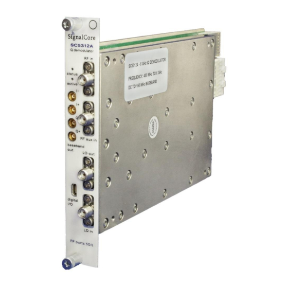
SC5312A & SC5313A Hardware Manual Front Interface Indicators and Connectors The SC5312A is a PXIe-based RF downconverter with all user I/O located on the front face of the module as shown below. Rev 2.1 | SC5312A & SC5313A User Manual... -
Page 10: Power Connection
Physical Description The SC5313A is a core module-based IQ demodulator with all I/O connections and indicators located on the front face of the module as shown below. Power Connection Power to the SC5313A is provided to the device through a two-position screw terminal block connection. Proper operation of the device requires a +12 VDC source and ground return wires capable of delivering a minimum current of 1.5 amps. -
Page 11: Baseband Connections
Maximum input power is +10 dBm. Baseband Connections The SC5312A and SC5313A have four baseband output ports comprised of differential in-phase (I+ and I-) and differential quadrature (Q+ and Q-) outputs. Nominal differential output impedance is 100 The demodulator can also be configured for single-ended or differential IF output. When configured for single-ended operation, it is recommended to terminate the other half of the differential pair using a 50 ... -
Page 12: Reset Button (Pin Hole)
3 Functional Description Overview The SC5312A uses USB as its primary interface with an optional SPI or RS232 interface. The SC5313A is a PXIe version of the product. They are single-stage, direct conversion Inphase-Quadrature (IQ) demodulating mixers. They can operate as a single-stage downconverter or as an IQ demodulator. These modules operate in the 400 MHz to 6 GHz RF range with a typical 3 dB IF bandwidth of 160 MHz in single- stage converter mode and 320 MHz in IQ mode. - Page 13 RF AMP#3) is not driven too hard. Finally RF ATTEN#3 is used to control the level to the IQ demodulator when RF AMP#2 is enabled (switched into the signal path). Rev 2.1 | SC5312A & SC5313A User Manual SignalCore, Inc.
-
Page 14: If Input Section
6000 MHz IF Input Section The SC5312A and SC5313A require an external RF signal as their “Local Oscillator” (LO) for the frequency conversion process. The external RF signal must be connected to the “LO in” port. The typical required input level is -3 dBm to 3 dBm. These levels are required to sufficiently drive the IQ demodulator for good linearity performance and conversion loss. -
Page 15: If Output Section
Generally, increasing the voltage results in higher current consumption, and as a result the linearity improves. However slight adjustments to the voltage may improve the linearity further; this is dependent on the frequency and input power. Rev 2.1 | SC5312A & SC5313A User Manual SignalCore, Inc. -
Page 16: Hardware Registers
Hardware Registers 4 Hardware Registers The set of hardware registers of the downconverter may be divided into a configuration set and a query set; the configuration registers are write-only registers to set up the states of the device, while the query registers request the device to prepare and send back data associated with them. -
Page 17: Register 0X02 Set_Sys_Active
0 = Turns off the active LED Mode 1 = Turns on the active LED [7:1] Unused Set to zeros [7:0] Read back byte Read 1 byte back is required for PXIe and RS232 Rev 2.1 | SC5312A & SC5313A User Manual SignalCore, Inc. -
Page 18: Register 0X03 Synth_Mode (2 Bytes)
Hardware Registers Register 0x03 SYNTH_MODE (2 Bytes) This register configures the PLL loop gain of the local oscillator synthesizers. It also enables or disables faster tuning of the YIG based oscillator of LO1. Bytes written 2 Bytes read 1 Bits Type Name Width... -
Page 19: Register 0X11 If_Frequency
This register sets the value of the device attenuators. Bytes written 4 Bytes read 1 Bits Type Name Width Description [7:0] Attenuator value In 0.25 dB steps, i.e. LSB = 0.25 dB Rev 2.1 | SC5312A & SC5313A User Manual SignalCore, Inc. -
Page 20: Register 0X16 Signal_Path
Hardware Registers Bits Type Name Width Description The attenuator number: 0 = RF Atten #1 1 = RF Atten #2 The target [10:8] 2 = not used attenuator 3 = External IF input IF2 Atten 4 = IF3 Atten #1 5 = IF3 Atten #2 [23:11] Unused... -
Page 21: Register 0X17 Config_Auto_Gain
0 = Computation will leave the state of the RF amplifier unchanged 1 = Computation will change the state of the RF autoCntrlRfAmp amplifier to provide the best device configuration to meet the input parameter requirements Rev 2.1 | SC5312A & SC5313A User Manual SignalCore, Inc. -
Page 22: Register 0X18 Store_Default_State
Hardware Registers Bits Type Name Width Description 0 = Best signal-to-noise (SNR), least linear 1 = Better SNR, sufficiently linear [4:3] linearMode 2 = Better linearity, sufficient SNR 3 = Best linearity, least SNR [7:5] Unused Set to zeros Set the absolute level of the expected RF input [14:8] rfLevel level in dB. -
Page 23: Register 0X19 Device_Standby
RefOutEnable Reference out port enabled 0 = 10 MHz output Clk10Enable 1 = 100 MHz output Only on SC5307A to enable export of the 10 MHz PXI10Enable backplane clock Rev 2.1 | SC5312A & SC5313A User Manual SignalCore, Inc. -
Page 24: Register 0X1B Reference_Dac
Hardware Registers Bits Type Name Width Description [7:2] Unused Set to zeros [7:0] Read back byte Read 1 byte back is required for PXIe and RS232 Register 0x1B REFERENCE_DAC This register makes adjustments to the 10 MHz TCXO accuracy via DAC to its tuning port. Bytes written 4 Bytes read 1 Bits... -
Page 25: Register 0X1E User_Eeprom_Write
1 = IF1 frequency [50:48] Parameter 2 = IF2 frequency 3 = IF3 frequency [55:51] Unused Set to zeros [7:0] Read back byte Read 1 byte back is required for PXIe and RS232 Rev 2.1 | SC5312A & SC5313A User Manual SignalCore, Inc. -
Page 26: Query Registers
Hardware Registers Query Registers These are request for data registers, in that a request for certain data is made by writing to the specific register first, followed by reading back the requested data. Some registers may require instruction data to specify the type of data to return, while others do not need any. -
Page 27: Register 0X31 Get_Temperature
32 bits of read data. [63:32] Invalid data Ignore Register 0x32 GET_DEVICE_STATUS Write to this register to query the current operating conditions. Bytes written 2 Bytes read 8 Rev 2.1 | SC5312A & SC5313A User Manual SignalCore, Inc. - Page 28 Hardware Registers Bits Type Name Width Description [7:0] Unused Set to zeros Pll status: LO1 sum The summing PLL of LO1 Pll status: LO1 crs The coarse tuning PLL of LO1 Pll status: LO1 fine The fine tuning PLL of LO1 Pll status: LO2 Pll Status: LO3 Pll status: VCXO...
-
Page 29: Register 0X33 Get_Device_Info
[36] autoRfAmp [37] Reserved [63:38] Invalid data Ignore Register 0x33 GET_DEVICE_INFO Write to this register to query the device information such as serial number. Bytes written 2 Bytes read 8 Rev 2.1 | SC5312A & SC5313A User Manual SignalCore, Inc. - Page 30 Hardware Registers Bits Type Name Width Description 0: Product serial number and Interface type 1: Firmware and hardware revision 2: Calibration and manufacture date [3:0] DeviceInfo 3: Device interface 4: Manufacture date 5: Last calibration date [7:4] Unused Ignore [63:0] Data Information data (see Device Info data) Register 0x34 CAL_EEPROM_READ...
-
Page 31: Device Parameters Data And Format
1000 to obtain the result in Hertz. Attenuator values Each attenuator value is returned as one byte, and the LSB is in 0.25 dB. Divide each byte by 4 to obtain the result in dB. Rev 2.1 | SC5312A & SC5313A User Manual SignalCore, Inc. -
Page 32: Device Information Parameters And Format
Hardware Registers Signal Chain Configuration The signal chain configuration data is in the first 2 bytes, and their data is represented in the following table. Table 6. Signal chain configuration data representation Bit Description [0] Bypass Conversion [1] IF2 external port select [2] Bypass IF3 conversion [3] NA [4] IF2 filter selection 0 = 160 MHz, 1 = 80 MHz... - Page 33 The first 4 bytes represent the manufactured date and the last 4 bytes represent the last calibration date. The date format is outlined in the following table. Type Description Month [4:3] Year (i.e. 2016) Rev 2.1 | SC5312A & SC5313A User Manual SignalCore, Inc.
- Page 34 Section 2 Communication Interfaces and Calibration ©2013 Rev 2.1...
-
Page 35: Communication Interfaces
Bulk transfer Control Transfer The USB control transfer parameters are: ENDPOINT_IN 0x80 ENDPOINT_OUT 0x00 TYPE_VENDOR 0x40 RECIP_INTERFACE 0x01 Bulk Transfer The USB bulk transfer parameters are: ENDPOINT_IN 0x83 ENDPOINT_OUT 0x04 Rev 2.1 | SC5312A & SC5313A User Manual SignalCore, Inc. -
Page 36: Spi Interface
Communication Interfaces The bulk transfer from the host to the device operates on a loopback with a data buffer of 8 bytes. When a device register is addressed, and upon completion of the register task, such as changing frequency, it will send back 8 bytes, which the host must read to clear the transfer buffers. -
Page 37: Writing The Spi Bus
64 clock cycles; 1 byte for the device register (0x37) and 7 empty bytes (MOSI) to clock out the returned data (MISO). An example of reading the device RF parameters (IF3 frequency) from the device is shown in the following figure. Rev 2.1 | SC5312A & SC5313A User Manual SignalCore, Inc. -
Page 38: Rs232 Interface
Communication Interfaces 0x02 0x36 0x00 0x00 0x00 0x00 0x00 0x00 0x00 0x30 Invalid Invalid Byte 7 Byte 6 Byte 5 Byte 4 Byte 3 Byte 2 Byte 1 Byte 0 Request for IF frequency from the Clock out the 6 bytes with write to the GET_SERIAL_OUT_BUFFER register (0x36) GET_DEVICE_PARAM register Figure 5. -
Page 39: Reading From The Device Via Rs232
A simple driver using IO controls should be sufficient to read and write byte data to this block of addresses. Although SignalCore provides the driver and API for these products, information is provided here for users who may need to write drivers for a different operating system or a different driver. -
Page 40: Writing To The Device
Communication Interfaces Writing to the Device Bytes that are written to the device must go through the bridge chip. In this section, we will first look at the write cycle of each byte, and then the write cycle of each device register. Do note the difference between the bridge register addresses and the device register addresses. -
Page 41: Calibration
850 MHz, 17 points) in MHz 0x82C Float_32 Bypass Conversion Absolute gain at each freq Bypass Relative IF3#2 atten at each freq. a1_f0, a1_f1,…,a1_fN 0x870 17x30 2040 Float_32 a2_f0, a2_f1,…,a2_fN a30_f0, a30_f1,…,a30_fN Rev 2.1 | SC5312A & SC5313A User Manual SignalCore, Inc. -
Page 42: Absolute Conversion Gain
Calibration Offset Length Points Data Type Description address (Bytes) 0x1868 Float_32 IF2 ext absolute gain dB Relative IF2ext Attenuator attenuation, 1-30 dB, 1 0x186C Float_32 dB step 0x18F8 Float_32 RF calf req, 100-6200, every 100, in MHz 0x19F0 Float_32 RF absolute gain at every freq 0x1AE8 Float_32 Relative RF amp gain at every freq... -
Page 43: Gain Through The Bypass Rf Conversion Path
��(��1) and ��(��1) are the first and second order temperature �������� gain coefficients respectively for RF band 1, and �� and �� are the current temperature and Rev 2.1 | SC5312A & SC5313A User Manual SignalCore, Inc. - Page 44 Calibration calibration temperature respectively. Adding this correction to the previously calculated gain will compensate the value for temperature deviation. �� = �� + ���� − ���� − ����3 + ∆�� ������ ������������ ����������1 ����������1 �������� ©2013 Rev 2.1...
-
Page 45: Revision Table
SC5312A & SC5313A Hardware Manual Revision Table Revision Revision Date Description 1/15/17 Initial Release 5/12/17 Corrected Status parameters 6/13/19 Address removed 8/5/20 Updated formatting 12/7/22 Corrected torque range Rev 2.1 | SC5312A & SC5313A User Manual SignalCore, Inc.
Need help?
Do you have a question about the SC5312A and is the answer not in the manual?
Questions and answers