
Subscribe to Our Youtube Channel
Related Manuals for Texas Instruments ADS62P EVM Series


Summary of Contents for Texas Instruments ADS62P EVM Series
- Page 1 ADS62PXXEVM User's Guide Literature Number: SLAU237A May 2008 – Revised April 2009...
- Page 2 SLAU237A – May 2008 – Revised April 2009 Submit Documentation Feedback...
-
Page 3: Table Of Contents
Contents ..........................Overview ................ADS62PXX EVM Quick-Start Procedure ....................... Circuit Description ....................... Schematic Diagram ..................... ADC Circuit Function ....................TI ADC SPI Control Interface ................Installing the ADC SPI Control Software ................Setting Up the EVM for ADC SPI Control ................ - Page 4 www.ti.com List of Figures ......................ADS62PXX Jumpers ....................ADS62PXX Surface Jumpers ..................ADS62PXXEVM Power Distribution ..............CDCE72010 EEPROM Configuration Block Diagram ..................... Found New Hardware ...................... Window Logo Testing ....................Hardware Device Manager ....................... SPI Interface Screen ....................TSW1200 GUI Introduction ....................
- Page 5 www.ti.com List of Tables ........................Jumper List ................EVM Power Supply Jumper Description ....................EVM Power Supply Options ..................Analog Input Jumper description ....................EVM Analog Input Options ..................Clock Input Jumper Description ....................EVM Clock Input Options ................. ADS62PXX Frequently Used Registers ......................
-
Page 6: Overview
User's Guide SLAU237A – May 2008 – Revised April 2009 ADS62PXXEVM Overview This user’s guide gives a general overview of the evaluation module (EVM) and provides a general description of the features and functions to be considered while using this module. This manual is applicable to the ADS62P42/43/44/45/48/49, ADS62P22/23/24/25/28/29 and ADS62C15/17 analog to digital converters (ADC), which will be collectively referred to as ADS62PXX. -
Page 7: Jumper List
Overview www.ti.com Table 1. Jumper List Jumper Function Default Jumper Setting Interface Circuit Operational Amplifier THS4509 (Bypassed) SJP1 AMP_OUT+ SJP2 AMP_OUT- THS4509_PD SJP5 AMPIN- SJP3 AMPIN+ No Shunt ADC Circuit JP11 Parallel SDATA JP10 MODE (Internal or External reference and Gain JP12 selection) SCLK... -
Page 8: Circuit Description
Circuit Description www.ti.com Circuit Description Schematic Diagram The schematic diagram for the this EVM is attached at the end of this document. See the schematic or relevant section of this user's guide before changing any jumpers. ADC Circuit Function Selection of various modes of operation of the ADS62PXX EVM is most often controlled by jumpers on the EVM, either by placing shunts on 0.025-inch square jumper posts or by installation of surface mount 0Ω... -
Page 9: Ads62Pxx Surface Jumpers
Circuit Description www.ti.com Figure 2. ADS62PXX Surface Jumpers 2.2.1 ADC Operational Mode By default, the ADC is configured to operate in parallel-mode operation, since jumper (JP11) asserts a 3.3V state to the ADC reset pin. Consequently, the SW1 reset pushbutton must be pressed only when the device is configured in serial operation mode. -
Page 10: Ads62Pxxevm Power Distribution
Circuit Description www.ti.com Figure 3. ADS62PXXEVM Power Distribution 2.2.2 EVM Power Connections Power is supplied to the EVM through banana jacks. From this input power, several different ways of delivering power to the ADC and other EVM functions are available. Figure 3 shows a simplified representation of the power options available for the ADS62PXXEVM. -
Page 11: Evm Power Supply Jumper Description
Circuit Description www.ti.com Table 2. EVM Power Supply Jumper Description EVM Banana Jack Description Jumper Setting 6V to 36V power supply Input default-apply just 5V 1-2 → Connects 5.3V to input of TPS79501 JP16 TPS79501 INPUT SELECT 2-3 → TPS79501 Input connected to J10 2-3 →... -
Page 12: Analog Input Jumper Description
Circuit Description www.ti.com 2.2.2.3 Power Supply Option 3 Option 3 is used to evaluate ADC performance using an isolated AVDD and DVDD power supply for current-consumption measurements. This option must be used with caution, because reversing the power supply or connecting to the wrong connector can damage the EVM. One common use of this option is to measure the separate current consumption of the relative supplies under particular operating conditions. -
Page 13: Evm Analog Input Options
Circuit Description www.ti.com Table 5. EVM Analog Input Options Jumper Changes Voltage on J11 Evaluation Goal Analog signal to ADC Comments Option Required and J13 SJP1→ 1-2 SJP2 → 1-2 Evaluate ADC From J6 (Channel A) or SJP3 → No shunt performance using direct Do not connect Default... -
Page 14: Clock Input Jumper Description
Circuit Description www.ti.com Alternatively, the clock may be supplied by an onboard VCXO and CDCE72010 clock buffer. The CDCE72010 Clock Buffer has been factory programmed to output a clock to the ADC that is 1/4 the rate of the on-board VCXO. While using this clock option, a separate 20MHz reference clock must be supplied to the CDCE72010 by way of the Clock Input SMA connector J19 (Surface jumper SJP4 should be shorted to position 2-3 for this case). -
Page 15: Evm Clock Input Options
Circuit Description www.ti.com Table 7. EVM Clock Input Options Jumper Changes Frequency Input CDC Configuration EVM Option Evaluation Goal Comments Required on J19 Description J18 → 2-3 SJP4 → 1-2 Evaluate ADC SJP7 → 1-2 ADC’s Sampling performance using a Default SJP6 →... -
Page 16: Cdce72010 Eeprom Configuration Block Diagram
Circuit Description www.ti.com Figure 4. CDCE72010 EEPROM Configuration Block Diagram 2.2.4.3 Clock Option 3 Option 3 is used for a differential LVPECL clock. This configuration eliminates the need for a crystal filter. It uses the same EEPROM configuration as Option 2, but in this case, the ADC clock pins are connected to Y1N and Y1P. -
Page 17: Ti Adc Spi Control Interface
TI ADC SPI Control Interface www.ti.com TI ADC SPI Control Interface This section describes the software features of the EVM kit. The TI ADC SPI control software provides full control of the SPI interface, allowing users to write to any of the ADC registers found in the data sheet. For most ADS62PXX performance evaluations, users do not need to use the TI SPI control software. -
Page 18: Setting Up The Evm For Adc Spi Control
TI ADC SPI Control Interface www.ti.com Figure 6. Window Logo Testing Figure 7. Hardware Device Manager Setting Up the EVM for ADC SPI Control Users who wish to use the ADC SPI interface must supply 5 VDC to P5, which provides power to the USB circuit. -
Page 19: Using The Ti Adc Spi Interface Software
TI ADC SPI Control Interface www.ti.com Using the TI ADC SPI Interface Software Once the software is installed and the USB cable is connected, three primary modes of operating the software are available: SPI Register Writes, SPI Register Write Using a Script File, and ADS62PXX Frequently Used Registers. -
Page 20: Ads62Pxx Frequently Used Registers
TI ADC SPI Control Interface www.ti.com 3.3.1 SPI Register Writes The most basic mode of operation allows full control of writing to individual register addresses. From the tabs at the top of the interface screen (Figure 8), select the ADS62PXX ADC. Next, type the Address Bytes(s) in hexadecimal (hex) and Data Byte(s) in hex, which can be found in the device data sheet. -
Page 21: Connecting To Fpga Platforms
Connecting to FPGA Platforms www.ti.com Connecting to FPGA Platforms The ADS62PXX EVM provides several connection options to use the EVM with various FPGA development platforms and FPGA-based capture boards. The ADC features two output options, a DDR LVDS which interfaces with a TSW1200 capture card, and a CMOS output which interfaces with a TSW1100 capture card. -
Page 22: Quick-Setup Test Result
Connecting to FPGA Platforms www.ti.com 4.1.1 Quick-Test Results The user can make the jumper setting as mentioned in Table 1. In this configuration, the EVM uses an external clock source from J19 and a direct input signal J6 (Channel A) or J3 (Channel B) to the ADC. This setup uses Power Option 2 (Table 3), Analog Input Option 1... -
Page 23: Adc Performance With Clock Through Onboard Vcxo, Cdce72010 And Crystal Filter
Connecting to FPGA Platforms www.ti.com 4.1.2 Test Result With Onboard VCXO and Clock Through Crystal Filter This test uses the VCXO of frequency 983.04 MHz. This setup uses the Power Option 2 (Table 3), Analog Input Option 1 (Table 5), and Clock Option 2 (Table 7). -
Page 24: Tsw1100
Connecting to FPGA Platforms www.ti.com 4.1.3 Test Result With Onboard VCXO and Differential LVPECL Clock For the same setup as explained in the previous section, when Clock Option 3 (Table 7) was used, the FFT was captured as shown in Figure 12. -
Page 25: Adc Evaluation
ADC Evaluation www.ti.com ADC Evaluation This section describes how to set up a typical ADC evaluation system that is similar to what TI uses to perform testing for data-sheet generation. Consequently, the information in this section is generic in nature and is applicable to all high-speed, high-resolution ADC evaluations. -
Page 26: Coherent Input Frequency Selection
ADC Evaluation www.ti.com Coherent Input Frequency Selection Typical ADC analysis requires users to collect the resulting time-domain data and perform a Fourier transform to analyze the data in the frequency domain. A stipulation of the Fourier transform is that the signal must be continuous-time;... -
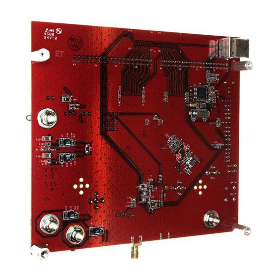
Page 27: Physical Description
Physical Description www.ti.com Physical Description This section describes the physical characteristics and PCB layout of the EVM. PCB Layout The EVM is constructed on a four-layer, 0.062-inch thick PCB using FR-4 material. The individual layers are shown in Figure 13 through Figure 18. -
Page 28: Component Side
Physical Description www.ti.com Figure 14. Component Side Figure 15. Power Plane 1 ADS62PXXEVM SLAU237A – May 2008 – Revised April 2009 Submit Documentation Feedback... -
Page 29: Layer
Physical Description www.ti.com Figure 16. Layer 2 Figure 17. Layer 3 SLAU237A – May 2008 – Revised April 2009 ADS62PXXEVM Submit Documentation Feedback... -
Page 30: Bottom Side
Physical Description www.ti.com Figure 18. Bottom Side ADS62PXXEVM SLAU237A – May 2008 – Revised April 2009 Submit Documentation Feedback... -
Page 31: Bill Of Materials
Physical Description www.ti.com Bill of Materials Table 9. Bill of Materials Reference Value Footprint Part Number DNI = Do Not Install C1,C6,C43,C64 1µF Panasonic ECJ-1VB1A105K C2, C8, C19–C23, C52–C59 0.1µF Panasonic ECJ-1VB1C104K C3, C5, C7, C10 22µF smd_cap_1210_pol Kemet T491A226M010AT C4, C9 10µF smd_cap_1210_pol... - Page 32 5001 TP3–TP6 T POINT R TESTPOINT Keystone 5002 T1–T5 WBC1-1TL XFMR_TC4-1W Coilcraft WBC1-1TL TC1-1T XFMR_TC4-1W Minicircuits TC1-1T THS4509 QFN16 Texas Instruments THS4509RGTT ADS62PXX QFN64 Texas Instruments ADS62PXX 93C66B TSSOP8 Microchip 93C66B FT245BM PQFP32 Future Technology FT245BM Devices U5, U7 TPS79633DCQ...
-
Page 33: Evm Schematics
Physical Description www.ti.com EVM Schematics Figure 19. EVM Schematic, Sheet 1 SLAU237A – May 2008 – Revised April 2009 ADS62PXXEVM Submit Documentation Feedback... -
Page 34: Evm Schematic, Sheet
Physical Description www.ti.com Figure 20. EVM Schematic, Sheet 2 ADS62PXXEVM SLAU237A – May 2008 – Revised April 2009 Submit Documentation Feedback... -
Page 35: Evm Schematic, Sheet
Physical Description www.ti.com Figure 21. EVM Schematic, Sheet 3 SLAU237A – May 2008 – Revised April 2009 ADS62PXXEVM Submit Documentation Feedback... -
Page 36: Evm Schematic, Sheet
Physical Description www.ti.com Figure 22. EVM Schematic, Sheet 4 ADS62PXXEVM SLAU237A – May 2008 – Revised April 2009 Submit Documentation Feedback... -
Page 37: Evm Schematic, Sheet
Physical Description www.ti.com Figure 23. EVM Schematic, Sheet 5 SLAU237A – May 2008 – Revised April 2009 ADS62PXXEVM Submit Documentation Feedback... -
Page 38: Breakout Board Schematic, Sheet
Physical Description www.ti.com Figure 24. Breakout Board Schematic, Sheet 6 ADS62PXXEVM SLAU237A – May 2008 – Revised April 2009 Submit Documentation Feedback... - Page 39 EVALUATION BOARD/KIT IMPORTANT NOTICE Texas Instruments (TI) provides the enclosed product(s) under the following conditions: This evaluation board/kit is intended for use for ENGINEERING DEVELOPMENT, DEMONSTRATION, OR EVALUATION PURPOSES ONLY and is not considered by TI to be a finished end-product fit for general consumer use. Persons handling the product(s) must have electronics training and observe good engineering practice standards.
-
Page 40: Important Notices
IMPORTANT NOTICE Texas Instruments Incorporated and its subsidiaries (TI) reserve the right to make corrections, modifications, enhancements, improvements, and other changes to its products and services at any time and to discontinue any product or service without notice. Customers should obtain the latest relevant information before placing orders and should verify that such information is current and complete.
Need help?
Do you have a question about the ADS62P EVM Series and is the answer not in the manual?
Questions and answers