Table of Contents
Advertisement
Quick Links
www.ti.com
User's Guide
ADS9817 Evaluation Module
This user's guide describes the characteristics, operation, and use of the ADS9817EVM evaluation module
(EVM). This kit is an evaluation platform for the ADS9817, which is an 8-channel, 18-bit, 2-MSPS per channel,
successive approximation register (SAR) analog-to-digital converter (ADC). The EVM eases the evaluation of
the ADS9817 device with hardware, software, and computer connectivity through the universal serial bus (USB)
interface. This user's guide includes complete circuit descriptions, schematic diagrams, and a bill of materials
(BOM). Throughout this document, the terms demonstration kit, evaluation board, evaluation module, and EVM
are synonymous with the ADS9817EVM.
SBAU416A – NOVEMBER 2022 – REVISED JULY 2023
Submit Document Feedback
ABSTRACT
ADS9817EVM Evaluation Module
Copyright © 2023 Texas Instruments Incorporated
ADS9817 Evaluation Module
1
Advertisement
Table of Contents

Related Manuals for Texas Instruments ADS9817


Summary of Contents for Texas Instruments ADS9817
- Page 1 This user's guide describes the characteristics, operation, and use of the ADS9817EVM evaluation module (EVM). This kit is an evaluation platform for the ADS9817, which is an 8-channel, 18-bit, 2-MSPS per channel, successive approximation register (SAR) analog-to-digital converter (ADC). The EVM eases the evaluation of the ADS9817 device with hardware, software, and computer connectivity through the universal serial bus (USB) interface.
-
Page 2: Table Of Contents
Figure 7-3. Digital Connector Schematic........................... Figure 7-4. ADS9817 PCB Layout (Top Layer)..........................22 Figure 7-5. ADS9817 PCB GND1 Layer (Signal Layer 1)......................Figure 7-6. ADS9817 PCB GND2 Layer (Signal Layer 2)......................Figure 7-7. ADS9817 PCB Layout (Bottom Layer)........................List of Tables Table 1-1. -
Page 3: Overview
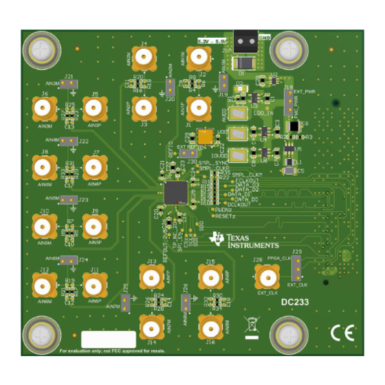
Overview 1 Overview The ADS9817EVM is a platform for evaluating the performance of the ADS9817 SAR ADC, which includes a PGA front-end to support input voltages of ±12-V, ±10-V, ±7-V, ±5-V, ±3.5-V, and ±2.5-V, both in single-ended and differential configurations. The ADC core supports 18-bit resolution at 2-MSPS/channel. The evaluation... -
Page 4: Figure 1-2. System Using Gui And Tswdc155Evm
Reference ADS9817 AIN7M AIN7P connector Clock Select AIN7P AIN8P AIN7M AIN7P External Clock AIN7M AIN8M Figure 1-3. ADS9817EVM Block Diagram ADS9817 Evaluation Module SBAU416A – NOVEMBER 2022 – REVISED JULY 2023 Submit Document Feedback Copyright © 2023 Texas Instruments Incorporated... -
Page 5: Ads9817Evm Quick Start Guide
ADS9817EVM Quick Start Guide 2 ADS9817EVM Quick Start Guide The following instructions are a step-by-step guide to connecting the ADS9817EVM to the computer and evaluating the performance of the ADS9817: 1. Review the default jumper settings in Figure 2-2 below as well as the power guidelines in Section 5.1. -
Page 6: Figure 2-2. Initial Required Setup On The Config Tab
ADS9817EVM Quick Start Guide www.ti.com Figure 2-2. Initial Required Setup on the Config Tab ADS9817 Evaluation Module SBAU416A – NOVEMBER 2022 – REVISED JULY 2023 Submit Document Feedback Copyright © 2023 Texas Instruments Incorporated... -
Page 7: Analog Interface
PSRR, low drop-out voltage and excellent load and line regulation to help meet strict transient requirements. The REF7040 on the EVM is the 4.096-V output voltage option. To connect the REF7040 to the ADS9817, configure the REFIO pin as an input via the GUI and then install a shunt on jumper J30. -
Page 8: Digital Interface And Clock Inputs
4.1 Digital Interface Connections The ADS9817 uses an SPI to configure the internal device registers (SCLK, SDI, SDO, CSn, and SPI_EN). A separate CMOS interface is used for capturing conversion data for each ADC channel using up to four output data lanes (D0, D1, D2, and D3). -
Page 9: Figure 4-2. Connections To Ads9817
REFM DVDD_1V8 REFM DVDD_1V8 1V8_VDD IOVDD IOVDD IOGND IOGND 0.1µF Thermal_Pad 1V8_IOVDD ADS9817IRSHT 0.1µF 0.1µF Figure 4-2. Connections to ADS9817 SBAU416A – NOVEMBER 2022 – REVISED JULY 2023 ADS9817 Evaluation Module Submit Document Feedback Copyright © 2023 Texas Instruments Incorporated... -
Page 10: Clock Select
(FMC_SMPL_CLKM) or GND through R22 or R35, respectively. By default, R35 is populated and R22 is uninstalled. EXT_SMPL_CLKP MNT_1 MNT_2 MNT_3 MNT_4 60312002114503 EXT_SMPL_CLKP SMPL_CLKP FMC_SMPL_CLKP FMC_SMPL_CLKM SMPL_CLKM Figure 4-3. Sample Clock Selection ADS9817 Evaluation Module SBAU416A – NOVEMBER 2022 – REVISED JULY 2023 Submit Document Feedback Copyright © 2023 Texas Instruments Incorporated... -
Page 11: Power Supplies
5-V supply. USB hubs can cause possible device enumeration issues and are not recommended when communicating through the TSWDC155EVM. SBAU416A – NOVEMBER 2022 – REVISED JULY 2023 ADS9817 Evaluation Module Submit Document Feedback Copyright © 2023 Texas Instruments Incorporated... -
Page 12: Ads9817Evm Software Reference
Typically, the default values work, but these values can be customized as needed based on the user's requirements. Figure 6-1. Initial Software Installation ADS9817 Evaluation Module SBAU416A – NOVEMBER 2022 – REVISED JULY 2023 Submit Document Feedback Copyright © 2023 Texas Instruments Incorporated... -
Page 13: Figure 6-2. Installation Process
This process takes a few minutes. At completion, the user can launch a readme text file and the application. Figure 6-2 shows these steps. Figure 6-2. Installation Process SBAU416A – NOVEMBER 2022 – REVISED JULY 2023 ADS9817 Evaluation Module Submit Document Feedback Copyright © 2023 Texas Instruments Incorporated... -
Page 14: Usb Driver Installation
5. Click on Have Disk in the pop-up window and navigate to C:\Program Files\Texas Instruments\ADS98xx\bin\proj_lib\Sparrow\Bootloader. Figure 6-3. Open Device Manager Figure 6-4. Update Driver With Device Manager ADS9817 Evaluation Module SBAU416A – NOVEMBER 2022 – REVISED JULY 2023 Submit Document Feedback Copyright © 2023 Texas Instruments Incorporated... -
Page 15: Using The Config Tab
Program FPGA buttons, some status LEDs on the hardware illuminate. The power-up step takes the longest time (approximately 30 seconds). After all four buttons are pressed, the power on the ADS9817EVM is on and the ADS9817 device registers are configured. Figure 6-5. Initial Required Setup on the Config Tab SBAU416A –... -
Page 16: Using The Capture Tab
Select the appropriate tab to view data for channel 1 or channel 2. Figure 6-6. Initial Required Setup on the Capture Tab ADS9817 Evaluation Module SBAU416A – NOVEMBER 2022 – REVISED JULY 2023 Submit Document Feedback Copyright © 2023 Texas Instruments Incorporated... -
Page 17: Using The Inl/Dnl Tool
Select the channel to measure and the hits per code, then press the GET INL/DNL button (as shown in Figure 6-7) to run this tool. Figure 6-7. Using the INL/DNL Tool SBAU416A – NOVEMBER 2022 – REVISED JULY 2023 ADS9817 Evaluation Module Submit Document Feedback Copyright © 2023 Texas Instruments Incorporated... -
Page 18: Using The Histogram Tab
As a result, saving the raw codes from the capture tab and processing the raw data is recommended. Figure 6-8. Using the Histogram Tab ADS9817 Evaluation Module SBAU416A – NOVEMBER 2022 – REVISED JULY 2023 Submit Document Feedback Copyright © 2023 Texas Instruments Incorporated... -
Page 19: Schematics, Layouts, And Bill Of Materials
7.1 Schematics Figure 7-1 through Figure 7-2 show the various connections to the ADS9817 device. The digital signals connect to J27, and the analog signals connect to SMA connectors and input filtering. Figure 7-1 also shows the decoupling for the device. -
Page 20: Figure 7-2. Power Connections And Regulators Schematic
1µF 1µF VOUT IOVDD 10uF 1.96M TPS61070DDCR 1V8_IOVDD 22µF 200k TPS7A2018PDBVR 1µF 1µF Figure 7-2. Power Connections and Regulators Schematic ADS9817 Evaluation Module SBAU416A – NOVEMBER 2022 – REVISED JULY 2023 Submit Document Feedback Copyright © 2023 Texas Instruments Incorporated... -
Page 21: Figure 7-3. Digital Connector Schematic
FMC_SMPL_CLKM SPI_EN 3P3VAUX SCLK 3P3V SMPL_SYNC 3P3V 3P3V VADJ VADJ ASP-134488-01 ASP-134488-01 ASP-134488-01 ASP-134488-01 ASP-134488-01 Figure 7-3. Digital Connector Schematic SBAU416A – NOVEMBER 2022 – REVISED JULY 2023 ADS9817 Evaluation Module Submit Document Feedback Copyright © 2023 Texas Instruments Incorporated... -
Page 22: Layout
Figure 7-7 shows the bottom layer for the EVM PCB layout. Figure 7-4. ADS9817 PCB Layout (Top Layer) Figure 7-5. ADS9817 PCB GND1 Layer (Signal Layer 1) ADS9817 Evaluation Module SBAU416A – NOVEMBER 2022 – REVISED JULY 2023 Submit Document Feedback... -
Page 23: Figure 7-6. Ads9817 Pcb Gnd2 Layer (Signal Layer 2)
Schematics, Layouts, and Bill of Materials Figure 7-6. ADS9817 PCB GND2 Layer (Signal Layer 2) Figure 7-7. ADS9817 PCB Layout (Bottom Layer) SBAU416A – NOVEMBER 2022 – REVISED JULY 2023 ADS9817 Evaluation Module Submit Document Feedback Copyright © 2023 Texas Instruments Incorporated... -
Page 24: Bill Of Materials (Bom)
Terminal Block, 3.5mm Pitch, 2x1, TH 7.0x8.2x6.5mm ED555/2DS On-Shore Technology J18, J29 Header, 100mil, 3x1, Gold, TH Header, 100mil, 3x1, TH HTSW-103-07-G-S Samtec ADS9817 Evaluation Module SBAU416A – NOVEMBER 2022 – REVISED JULY 2023 Submit Document Feedback Copyright © 2023 Texas Instruments Incorporated... - Page 25 TPS61070DDCR Texas Instruments DDC0006A (SOT-23-T-6) 2 ppm/°C Maximum Drift, 0.23 ppmp-p 1/f LCCC8 REF7040QFKHT Texas Instruments Noise, Precision Voltage Reference SBAU416A – NOVEMBER 2022 – REVISED JULY 2023 ADS9817 Evaluation Module Submit Document Feedback Copyright © 2023 Texas Instruments Incorporated...
- Page 26 RES, 10 k, 5%, 0.063 W, 0402 0402 CRCW040210K0JNED Vishay-Dale R26, R31, R32 RES, 0, 5%, 0.1 W, AEC-Q200 Grade 0, 0402 ERJ-2GE0R00X Panasonic 0402 ADS9817 Evaluation Module SBAU416A – NOVEMBER 2022 – REVISED JULY 2023 Submit Document Feedback Copyright © 2023 Texas Instruments Incorporated...
-
Page 27: Revision History
Added Using the Histogram Tab section......................• Changed schematic images..........................• Changed Layout images...........................22 • Changed the Bill of Materials table........................24 SBAU416A – NOVEMBER 2022 – REVISED JULY 2023 ADS9817 Evaluation Module Submit Document Feedback Copyright © 2023 Texas Instruments Incorporated... - Page 28 STANDARD TERMS FOR EVALUATION MODULES Delivery: TI delivers TI evaluation boards, kits, or modules, including any accompanying demonstration software, components, and/or documentation which may be provided together or separately (collectively, an “EVM” or “EVMs”) to the User (“User”) in accordance with the terms set forth herein.
- Page 29 www.ti.com Regulatory Notices: 3.1 United States 3.1.1 Notice applicable to EVMs not FCC-Approved: FCC NOTICE: This kit is designed to allow product developers to evaluate electronic components, circuitry, or software associated with the kit to determine whether to incorporate such items in a finished product and software developers to write software applications for use with the end product.
- Page 30 www.ti.com Concernant les EVMs avec antennes détachables Conformément à la réglementation d'Industrie Canada, le présent émetteur radio peut fonctionner avec une antenne d'un type et d'un gain maximal (ou inférieur) approuvé pour l'émetteur par Industrie Canada. Dans le but de réduire les risques de brouillage radioélectrique à...
- Page 31 www.ti.com EVM Use Restrictions and Warnings: 4.1 EVMS ARE NOT FOR USE IN FUNCTIONAL SAFETY AND/OR SAFETY CRITICAL EVALUATIONS, INCLUDING BUT NOT LIMITED TO EVALUATIONS OF LIFE SUPPORT APPLICATIONS. 4.2 User must read and apply the user guide and other available documentation provided by TI regarding the EVM prior to handling or using the EVM, including without limitation any warning or restriction notices.
- Page 32 Notwithstanding the foregoing, any judgment may be enforced in any United States or foreign court, and TI may seek injunctive relief in any United States or foreign court. Mailing Address: Texas Instruments, Post Office Box 655303, Dallas, Texas 75265 Copyright © 2023, Texas Instruments Incorporated...
- Page 33 TI products. TI’s provision of these resources does not expand or otherwise alter TI’s applicable warranties or warranty disclaimers for TI products. TI objects to and rejects any additional or different terms you may have proposed. IMPORTANT NOTICE Mailing Address: Texas Instruments, Post Office Box 655303, Dallas, Texas 75265 Copyright © 2023, Texas Instruments Incorporated...
Need help?
Do you have a question about the ADS9817 and is the answer not in the manual?
Questions and answers