Table of Contents
Advertisement
Quick Links
One Technology Way • P.O. Box 9106 • Norwood, MA 02062-9106, U.S.A. • Tel: 781.329.4700 • Fax: 781.461.3113 • www.analog.com
Evaluation Board for the
FEATURES
Full featured evaluation board for the
Single board with both 50 Ω and 75 Ω termination
±5 V operation
EVALUATION KIT CONTENTS
ADV3221-EVALZ/ADV3222-EVALZ
Instruction guide for user guide download
EQUIPMENT NEEDED
Signal source or video pattern generator and signal analyzer
Power supplies (2 V/100 mA and ±5 V/1 A)
BNC-to-SMA connector for inputs and output using the 50 Ω
terminated board
BNC-to-BNC connector for inputs and output using the 75 Ω
terminated board
GENERAL DESCRIPTION
The
ADV3221
and
ADV3222
buffered, 4:1 analog multiplexers. They offer a −3 dB signal
bandwidth greater than 800 MHz and channel switch times of
less than 20 ns with 1% settling. With lower than −58 dB of
crosstalk and −67 dB isolation (at 100 MHz), the
ADV3222
are useful in many high speed applications. The
PLEASE SEE THE LAST PAGE FOR AN IMPORTANT
WARNING AND LEGAL TERMS AND CONDITIONS.
ADV3221-EVALZ/ADV3222-EVALZ User Guide
ADV3221/ADV3222
ADV3221/ADV3222
evaluation board
are high speed, high slew rate,
ADV3221
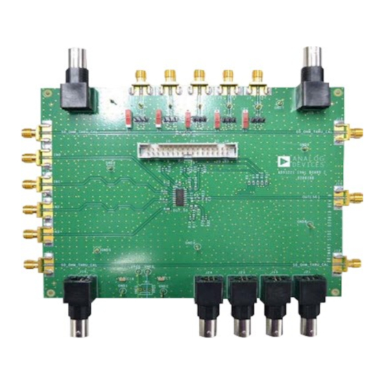
EVALUATION BOARD PHOTOGRAPH AND BLOCK DIAGRAM
800 MHz, 4:1 Analog Multiplexers
differential gain error of less than 0.02% and differential phase
error of less than 0.02°, together with 0.1 dB gain flatness out to
100 MHz while driving a 75 Ω back terminated load, make the
ADV3221
and
The
ADV3221/ADV3222
placed into a high impedance state, which allows multiple
outputs to be connected together for cascading stages without
the off channels loading the output bus. The
gain of +1, and the
operate on ±5 V supplies while consuming less than 7.5 mA of
idle current. The channel switching is performed via latched
control lines, allowing synchronous updating in a multiple
ADV3221/ADV3222
The
ADV3221/ADV3222
and are available over the extended industrial temperature range
of −40°C to +85°C.
This user guide provides all of the supporting documentation
for working with the
evaluation board. Additional information is available in the
ADV3221/ADV3222
conjunction with this user guide when working with the
and
evaluation board.
D
Q
CS
LATCH
D
Q
A0
LATCH
D
Q
A1
LATCH
CK1
CK2
100kΩ
Figure 1.
Rev. 0 | Page 1 of 10
ADV3222
ideal for all types of signal switching.
include an output buffer that can be
ADV3222
has a gain of +2; both devices
environment.
are offered in a 16-lead SOIC package
ADV3221-EVALZ/ADV3222-EVALZ
data sheet, which should be consulted in
ENABLE
D
Q
LATCH
IN0
D
Q
IN1
IN2
LATCH
IN3
D
Q
LATCH
100kΩ
UG-844
ADV3221
has a
G = +1
OUT
(G = +2)
Advertisement
Table of Contents

Related Manuals for Analog Devices ADV3221-EVALZ


Summary of Contents for Analog Devices ADV3221-EVALZ
-
Page 1: Features
ADV3221-EVALZ/ADV3222-EVALZ User Guide UG-844 One Technology Way • P.O. Box 9106 • Norwood, MA 02062-9106, U.S.A. • Tel: 781.329.4700 • Fax: 781.461.3113 • www.analog.com Evaluation Board for the ADV3221/ADV3222 800 MHz, 4:1 Analog Multiplexers differential gain error of less than 0.02% and differential phase FEATURES error of less than 0.02°, together with 0.1 dB gain flatness out to... -
Page 2: Table Of Contents
UG-844 ADV3221-EVALZ/ADV3222-EVALZ User Guide TABLE OF CONTENTS Features ....................1 Power Supply ..................3 Evaluation Kit Contents ..............1 Analog Inputs.................3 Equipment Needed ................1 Analog Output ................3 General Description ................. 1 Digital Logic Inputs ..............3 Evaluation Board Photograph and Block Diagram...... 1 Quick Start Guide ................3... -
Page 3: Evaluation Board Hardware
ADV3221-EVALZ/ADV3222-EVALZ User Guide UG-844 EVALUATION BOARD HARDWARE INTRODUCTION QUICK START GUIDE ADV3221-EVALZ/ADV3222-EVALZ evaluation board To get started, take the following steps: allows the user to easily evaluate the ADV3221/ADV3222 Remove the ADV3221-EVALZ/ADV3222-EVALZ both the 50 Ω and 75 Ω terminations. Figure 2 shows the typical evaluation board from the box. - Page 4 UG-844 ADV3221-EVALZ/ADV3222-EVALZ User Guide OSCILLOSCOPE THRU CAL (75Ω) ANALOG OUTPUT (75Ω) DIGITAL LOGIC INPUTS THRU CAL (50Ω) OSCILLOSCOPE WAVEFORM/SIGNAL GENERATOR ANALOG INPUTS (50Ω) ANALOG OUTPUT (50Ω) THRU CAL (75Ω) ANALOG INPUT (75Ω) DC POWER SUPPLY VIDEO PATTERN GENERATOR Figure 2. Typical Evaluation Setup...
-
Page 5: Evaluation Board Schematics And Artwork
ADV3221-EVALZ/ADV3222-EVALZ User Guide UG-844 EVALUATION BOARD SCHEMATICS AND ARTWORK Figure 3. Evaluation Board Schematic, 50 Ω Terminated Side Rev. 0 | Page 5 of 10... - Page 6 UG-844 ADV3221-EVALZ/ADV3222-EVALZ User Guide Figure 4. Evaluation Board Schematic, Supplies, and Thru Cal Rev. 0 | Page 6 of 10...
- Page 7 ADV3221-EVALZ/ADV3222-EVALZ User Guide UG-844 Figure 5. Evaluation Board Schematic, 75 Ω Terminated Side Rev. 0 | Page 7 of 10...
- Page 8 UG-844 ADV3221-EVALZ/ADV3222-EVALZ User Guide Figure 6. ADV3221-EVALZ/ADV3222-EVALZ Evaluation Board, Top View Figure 7. ADV3221-EVALZ/ADV3222-EVALZ Evaluation Board, Bottom View Rev. 0 | Page 8 of 10...
-
Page 9: Ordering Information
ADV3221-EVALZ/ADV3222-EVALZ User Guide UG-844 ORDERING INFORMATION BILL OF MATERIALS Table 2. Reference Item Description Manufacturer Manufacturer Part No. Designator Capacitor, ceramic, chip, X8R, 0.1 µF C1608X8R1E104K C1, C2, C8, C17, C28, C29 Capacitor, ceramic, monolithic, X5R,10 µF Murata GRM31CR61E106KA12L C7, C16 Capacitor, ceramic, X7R, 0.01 µF... - Page 10 By using the evaluation board discussed herein (together with any tools, components documentation or support materials, the “Evaluation Board”), you are agreeing to be bound by the terms and conditions set forth below (“Agreement”) unless you have purchased the Evaluation Board, in which case the Analog Devices Standard Terms and Conditions of Sale shall govern. Do not use the Evaluation Board until you have read and agreed to the Agreement.
Need help?
Do you have a question about the ADV3221-EVALZ and is the answer not in the manual?
Questions and answers