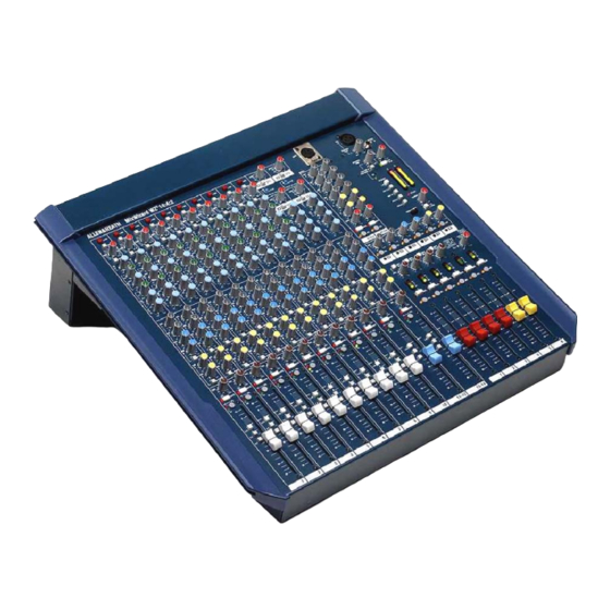
ALLEN & HEATH 14:4:2 MixWizard WZ3 Service Information
Hide thumbs
Also See for 14:4:2 MixWizard WZ3:
- User manual (34 pages) ,
- User manual (27 pages) ,
- User manual (22 pages)
Advertisement
Quick Links
Advertisement

Related Manuals for ALLEN & HEATH 14:4:2 MixWizard WZ3


Summary of Contents for ALLEN & HEATH 14:4:2 MixWizard WZ3
- Page 1 MixWizard WZ 14:4:2 SERVICE INFORMATION Publication AP5938...
-
Page 2: Additional Resources
Introduction This publication provides technical information on servicing the Allen & Heath WZ 14:4:2. Included are internal layout drawing, block diagram and circuit schematics with board layouts and spare parts lists. Whilst we believe this information to be reliable we do not assume responsibility for inaccuracies. -
Page 3: Operation
Servicing Precautions – General Notes Service personnel: Service work should be carried out by technically qualified service personnel only. Mains power is dangerous and can kill. Do not attempt to work on a linear or switched mode power supply if you are not suitably qualified to do so. Do not attempt to repair surface mount circuit assemblies unless you are suitably qualified and have the necessary facilities to do so. - Page 4 Contents Log Internal Layout drawing ........... wz3-1442_layout_1.pdf Surface and Main Parts..........wz3-1442_parts_1.pdf System Block Diagram ........wz3-1442_blockdiagram_1.pdf Power Supply PCB........wz3-1442_003-171_psu_3.pdf Mono Input PCB.......wz3-1442_003-208_mono_input_2.pdf Connector PCB ........wz3-1442_003-209_connector_1.pdf .............wz3-1442_003-209_connector_2.pdf Group & Group / Matrix PCBs ....wz3-1442_003-210_group_1.3.pdf Stereo Input PCB ......wz3-1442_003-211_stereo_input_2.1.pdf Left PCB ............
- Page 5 14:4:2– Historical Change Log The following list identifies historical changes to the WZ 14:4:2. The effective dates, serial numbers and related change note documentation are included for reference to help identify the correct issue circuit boards and components. Whilst we believe this information to be reliable we do not assume responsibility for inaccuracies.
- Page 6 14:4:2 Internal Layout POWER / LEFT HARNESS AL5489 Product ......W31442/100 .......... W31442/110 .......... W31442/120 MASTER / RIGHT HARNESS AL5484 INPUT TO CONNECTOR HARNESS AL5463 .......... W31442/220 .......... W31442/240 Pack Assembly......003-164 INTERCONNECT STEREO HARNESS AL5633 INPUT Main Assembly ......003-205 PCBs 003-211 MONO INPUT PCBs...
- Page 7 14:4:2 Surface Parts 9MM POT NUT AB8050 LAMP RED PUSH BUTTON AJ2961 4x5/16 SCREW AB2810 LATCHING SWITCH AL0162 GAIN 4PIN FEMALE XLR AL8104 +48V 14MM 20KK X2 POT AI8007 3PIN FEMALE XLR AL2412 GREY PUSH BUTTON AJ2864 LATCHING SWITCH AL0162 (LINE) M3x6 SCREW AB0215 LATCHING SWITCH AL0162...
- Page 8 14:4:2 Surface Parts JACK SOCKET SWITCHED AL3410 ALLEN&HEATH MixWizard WZ 14:4:2 2-TRACK DUAL PHONO AL3240 13-14 11-12 RETURN SEND INSERT INSERT INSERT INSERT INSERT INSERT INSERT INSERT INSERT INSERT INSERT INSERT INSERT JACK SOCKET SWITCHED AL3410 LINE IN LINE IN LINE IN LINE IN LINE IN...
-
Page 9: Mic/Line Inputs
WZ3 14:4:2 SYS-LINK CONNECTION PHANTOM POWER 4 BAND EQUALISER GRP/AUX REV GAIN AUX OUT LINE (PAD) MUTE -20dB 2= + AUX MIX +10dB boost TIP= + BALANCED TIP= + GROUPS / AUX 1-4 IMPEDANCE BALANCED +4dBu BAL OPTION -2dBu FADER LINE METER TIP= SEND... - Page 10 HOLE-FIXING 3.5MM NTC1 CHOKE 20MH INRUSH SUPP NTC20R T500mA TP35 TP37 TP39 TP40 IEC MAINS INLET HOLE-FIXING 3.5MM+PAD TP33 FUSE HOLDER 20MM 2N2 250V/PEM TP34 HOLE-FIXING 3.5MM+PAD MAINS 1M2 1/2W 100N 275V/PEM Earth 100N 275V/PEM TP38 INLET TP41 TP36 Earth HOLE-FIXING 3.5MM+PAD 2N2 250V/PEM HOLE-FIXING 3.5MM+PAD...
- Page 11 003-171 iss.3 003-171...
- Page 12 SW1A SW2PCOL (SPUN) DIR_OUT+ 470R 0805 SW5B 4K7 1% 0805 MELF 68R 0805 SW2PCOL (SPUN) 4K7 1% 0805 MELF 330/10 TL072D SMD SW2A 68R 0805 AUX1 TL072D 100N 0805 SW2PCOL (SPUN) JP14 10K 1% 0805 VR1A 8K2 1% 0805 TL072D SMD JP1C SW5A POT14 5KRD X2...
- Page 13 003-208 iss.2...
- Page 14 C5399_1 CH1 C5399_1 CH2 C5399_1 CH3 C5399_1 CH4 C5399_1 CH5 C5399_1 CH6 C5399_1 CH7 C5399_1 CH8 C5399_1 CH1.Sch C5399_1 CH2.Sch C5399_1 CH3.Sch C5399_1 CH4.Sch C5399_1 CH5.Sch C5399_1 CH6.Sch C5399_1 CH7.Sch C5399_1 CH8.Sch C5399_1 CH9 C5399_1 CH10 C5399_1 STEREO C5399_1 GROUPS C5399_1 CH9.Sch C5399_1 CH10.Sch C5399_1 STEREO.Sch...
- Page 15 CN100 JACK V5M INSEND INSEND INSEND INSRET INSRET INSRET CN101 JACK V5M LINE+ LINE+ LINE+ LINE- LINE- LINE- C102 L100 MIC- MIC- MIC- R100 47/63 6K8 1% C100 15P/DISK +48V_SW +48V_SW +48V_SW C101 R101 15P/DISK 6K8 1% C103 L101 MIC+ MIC+ MIC+ 47/63...
- Page 16 CN100_1 JACK V5M INSEND INSEND INSEND INSRET INSRET INSRET CN101_1 JACK V5M LINE+ LINE+ LINE+ LINE- LINE- LINE- C102_1 L100_1 MIC- MIC- MIC- R100_1 47/63 6K8 1% C100_1 15P/DISK +48V_SW +48V_SW +48V_SW C101_1 R101_1 15P/DISK 6K8 1% C103_1 L101_1 MIC+ MIC+ MIC+ 47/63...
- Page 17 CN100_2 JACK V5M INSEND INSEND INSEND INSRET INSRET INSRET CN101_2 JACK V5M LINE+ LINE+ LINE+ LINE- LINE- LINE- C102_2 L100_2 MIC- MIC- MIC- R100_2 47/63 6K8 1% C100_2 15P/DISK +48V_SW +48V_SW +48V_SW C101_2 L101_2 R101_2 15P/DISK 6K8 1% C103_2 MIC+ MIC+ MIC+ 47/63...
- Page 18 CN100_3 JACK V5M INSEND INSEND INSEND INSRET INSRET INSRET CN101_3 JACK V5M LINE+ LINE+ LINE+ LINE- LINE- LINE- C102_3 L100_3 MIC- MIC- MIC- R100_3 47/63 6K8 1% C100_3 15P/DISK +48V_SW +48V_SW +48V_SW C101_3 R101_3 15P/DISK 6K8 1% C103_3 L101_3 MIC+ MIC+ MIC+ 47/63...
- Page 19 CN100_4 JACK V5M INSEND INSEND INSEND INSRET INSRET INSRET CN101_4 JACK V5M LINE+ LINE+ LINE+ LINE- LINE- LINE- C102_4 L100_4 MIC- MIC- MIC- R100_4 47/63 6K8 1% C100_4 15P/DISK +48V_SW +48V_SW +48V_SW C101_4 R101_4 15P/DISK 6K8 1% C103_4 L101_4 MIC+ MIC+ MIC+ 47/63...
- Page 20 CN100_5 JACK V5M INSEND INSEND INSEND INSRET INSRET INSRET CN101_5 JACK V5M LINE+ LINE+ LINE+ LINE- LINE- LINE- C102_5 L100_5 MIC- MIC- MIC- R100_5 47/63 6K8 1% C100_5 15P/DISK +48V_SW +48V_SW +48V_SW C101_5 R101_5 15P/DISK 6K8 1% C103_5 L101_5 MIC+ MIC+ MIC+ 47/63...
- Page 21 CN100_6 JACK V5M INSEND INSEND INSEND INSRET INSRET INSRET CN101_6 JACK V5M LINE+ LINE+ LINE+ LINE- LINE- LINE- C102_6 L100_6 MIC- MIC- MIC- R100_6 47/63 6K8 1% C100_6 15P/DISK +48V_SW +48V_SW +48V_SW C101_6 R101_6 15P/DISK 6K8 1% C103_6 L101_6 MIC+ MIC+ MIC+ 47/63...
- Page 22 CN100_7 JACK V5M INSEND INSEND INSEND INSRET INSRET INSRET CN101_7 JACK V5M LINE+ LINE+ LINE+ LINE- LINE- LINE- C102_7 L100_7 MIC- MIC- MIC- R100_7 47/63 6K8 1% C100_7 15P/DISK +48V_SW +48V_SW +48V_SW C101_7 R101_7 15P/DISK 6K8 1% C103_7 L101_7 MIC+ MIC+ MIC+ 47/63...
- Page 23 CN100_8 JACK V5M INSEND INSEND INSEND INSRET INSRET INSRET CN101_8 JACK V5M LINE+ LINE+ LINE+ LINE- LINE- LINE- C102_8 L100_8 MIC- MIC- MIC- R100_8 47/63 6K8 1% C100_8 15P/DISK +48V_SW +48V_SW +48V_SW C101_8 R101_8 15P/DISK 6K8 1% C103_8 L101_8 MIC+ MIC+ MIC+ 47/63...
- Page 24 CN100_9 JACK V5M INSEND INSEND INSEND INSRET INSRET INSRET CN101_9 JACK V5M LINE+ LINE+ LINE+ LINE- LINE- LINE- C102_9 L100_9 MIC- MIC- MIC- R100_9 47/63 6K8 1% C100_9 15P/DISK +48V_SW +48V_SW +48V_SW C101_9 R101_9 15P/DISK 6K8 1% C103_9 L101_9 MIC+ MIC+ MIC+ 47/63...
- Page 25 CN200 CN202 L200 L206 JACK V5M ST1_IN_R+ JACK V5M ST3_IN_R+ ST1_IN_L+ ST1_IN_L+ ST1_IN_R+ CN204 CN205 ST1_IN_R+ JACK V5M JACK V5M ST2_IN_L+ ST2_IN_L+ L201 L207 ST1_IN_L+ ST3_IN_L+ ST2_IN_L- ST2_IN_L- ST2_IN_R+ ST2_IN_R+ ST2_IN_R- ST2_IN_R- ST3_IN_L+ CN201 CN203 ST3_IN_L+ L202 L208 JACK V5M ST2_IN_R+ JACK V5M ST4_IN_R+...
- Page 26 CN300 CN301 CN302 CN303 JACK V5M INSEND_G1 JACK V5M INSEND_G2 JACK V5M INSEND_G3 JACK V5M INSEND_G4 INSEND_G1 INSEND_G2 INSEND_G3 INSEND_G4 INSRET_G1 INSRET_G2 INSRET_G3 INSRET_G4 INSRET_G1 INSRET_G2 INSRET_G3 INSRET_G4 C300 GROUP1_OUT+ C302 GROUP2_OUT+ C304 GROUP3_OUT+ C306 GROUP4_OUT+ GROUP1_OUT+ GROUP2_OUT+ GROUP3_OUT+ GROUP4_OUT+ 47/25 47/25 47/25...
- Page 27 CN400 CN401 JACK V5M INSEND_MIXL JACK V5M INSEND_MIXR INSRET_MIXL INSRET_MIXR CN407 CN405 CN406 JACK V3M LOCAL_MON_L C400 MIXL_OUT+ C402 MIXR_OUT+ C404 MONO_OUT+ RCA PHONO 2V R/W RCA PHONO 2V R/W 47/25 47/25 47/25 R406 R400 R402 R404 2TRK_IN_L 2TRK_OUT_L 100K 1% 100K 1% 100K 1% CN402...
- Page 28 003-209 iss.1...
- Page 29 C5399_2 CH1 C5399_2 CH2 C5399_2 CH3 C5399_2 CH4 C5399_2 CH5 C5399_2 CH6 C5399_2 CH7 C5399_2 CH8 C5399_2 CH1.Sch C5399_2 CH2.Sch C5399_2 CH3.Sch C5399_2 CH4.Sch C5399_2 CH5.Sch C5399_2 CH6.Sch C5399_2 CH7.Sch C5399_2 CH8.Sch C5399_2 CH9 C5399_2 CH10 C5399_2 STEREO C5399_2 GROUPS C5399_2 CH9.Sch C5399_2 CH10.Sch C5399_2 STEREO.Sch...
- Page 30 CN100 JACK V5M INSEND INSEND INSEND INSRET INSRET INSRET CN101 JACK V5M LINE+ LINE+ LINE+ LINE- LINE- LINE- C102 L100 MIC- MIC- MIC- R100 47/63 6K8 1% C100 15P/DISK +48V_SW +48V_SW +48V_SW C101 R101 15P/DISK 6K8 1% C103 L101 MIC+ MIC+ MIC+ 47/63...
- Page 31 CN100_1 JACK V5M INSEND INSEND INSEND INSRET INSRET INSRET CN101_1 JACK V5M LINE+ LINE+ LINE+ LINE- LINE- LINE- C102_1 L100_1 MIC- MIC- MIC- R100_1 47/63 6K8 1% C100_1 15P/DISK +48V_SW +48V_SW +48V_SW C101_1 R101_1 15P/DISK 6K8 1% C103_1 L101_1 MIC+ MIC+ MIC+ 47/63...
- Page 32 CN100_2 JACK V5M INSEND INSEND INSEND INSRET INSRET INSRET CN101_2 JACK V5M LINE+ LINE+ LINE+ LINE- LINE- LINE- C102_2 L100_2 MIC- MIC- MIC- R100_2 47/63 6K8 1% C100_2 15P/DISK +48V_SW +48V_SW +48V_SW C101_2 L101_2 R101_2 15P/DISK 6K8 1% C103_2 MIC+ MIC+ MIC+ 47/63...
- Page 33 CN100_3 JACK V5M INSEND INSEND INSEND INSRET INSRET INSRET CN101_3 JACK V5M LINE+ LINE+ LINE+ LINE- LINE- LINE- C102_3 L100_3 MIC- MIC- MIC- R100_3 47/63 6K8 1% C100_3 15P/DISK +48V_SW +48V_SW +48V_SW C101_3 R101_3 15P/DISK 6K8 1% C103_3 L101_3 MIC+ MIC+ MIC+ 47/63...
- Page 34 CN100_4 JACK V5M INSEND INSEND INSEND INSRET INSRET INSRET CN101_4 JACK V5M LINE+ LINE+ LINE+ LINE- LINE- LINE- C102_4 L100_4 MIC- MIC- MIC- R100_4 47/63 6K8 1% C100_4 15P/DISK +48V_SW +48V_SW +48V_SW C101_4 R101_4 15P/DISK 6K8 1% C103_4 L101_4 MIC+ MIC+ MIC+ 47/63...
- Page 35 CN100_5 JACK V5M INSEND INSEND INSEND INSRET INSRET INSRET CN101_5 JACK V5M LINE+ LINE+ LINE+ LINE- LINE- LINE- C102_5 L100_5 MIC- MIC- MIC- R100_5 47/63 6K8 1% C100_5 15P/DISK +48V_SW +48V_SW +48V_SW C101_5 R101_5 15P/DISK 6K8 1% C103_5 L101_5 MIC+ MIC+ MIC+ 47/63...
- Page 36 CN100_6 JACK V5M INSEND INSEND INSEND INSRET INSRET INSRET CN101_6 JACK V5M LINE+ LINE+ LINE+ LINE- LINE- LINE- C102_6 L100_6 MIC- MIC- MIC- R100_6 47/63 6K8 1% C100_6 15P/DISK +48V_SW +48V_SW +48V_SW C101_6 R101_6 15P/DISK 6K8 1% C103_6 L101_6 MIC+ MIC+ MIC+ 47/63...
- Page 37 CN100_7 JACK V5M INSEND INSEND INSEND INSRET INSRET INSRET CN101_7 JACK V5M LINE+ LINE+ LINE+ LINE- LINE- LINE- C102_7 L100_7 MIC- MIC- MIC- R100_7 47/63 6K8 1% C100_7 15P/DISK +48V_SW +48V_SW +48V_SW C101_7 R101_7 15P/DISK 6K8 1% C103_7 L101_7 MIC+ MIC+ MIC+ 47/63...
- Page 38 CN100_8 JACK V5M INSEND INSEND INSEND INSRET INSRET INSRET CN101_8 JACK V5M LINE+ LINE+ LINE+ LINE- LINE- LINE- C102_8 L100_8 MIC- MIC- MIC- R100_8 47/63 6K8 1% C100_8 15P/DISK +48V_SW +48V_SW +48V_SW C101_8 R101_8 15P/DISK 6K8 1% C103_8 L101_8 MIC+ MIC+ MIC+ 47/63...
- Page 39 CN100_9 JACK V5M INSEND INSEND INSEND INSRET INSRET INSRET CN101_9 JACK V5M LINE+ LINE+ LINE+ LINE- LINE- LINE- C102_9 L100_9 MIC- MIC- MIC- R100_9 47/63 6K8 1% C100_9 15P/DISK +48V_SW +48V_SW +48V_SW C101_9 R101_9 15P/DISK 6K8 1% C103_9 L101_9 MIC+ MIC+ MIC+ 47/63...
- Page 40 CN200 CN202 L200 L206 JACK V5M ST1_IN_L+ JACK V5M ST3_IN_L+ ST1_IN_L+ ST1_IN_L+ ST1_IN_R+ ST1_IN_R+ CN204 CN205 ST2_IN_L+ ST2_IN_L+ JACK V5M L201 JACK V5M L207 ST1_IN_R+ ST3_IN_R+ ST2_IN_L- ST2_IN_L- ST2_IN_R+ ST2_IN_R+ ST2_IN_R- ST2_IN_R- ST3_IN_L+ CN201 CN203 ST3_IN_L+ L202 L208 JACK V5M ST2_IN_L+ JACK V5M ST4_IN_L+...
- Page 41 CN300 CN301 CN302 CN303 JACK V5M INSEND_G1 JACK V5M INSEND_G2 JACK V5M INSEND_G3 JACK V5M INSEND_G4 INSEND_G1 INSEND_G2 INSEND_G3 INSEND_G4 INSRET_G1 INSRET_G2 INSRET_G3 INSRET_G4 INSRET_G1 INSRET_G2 INSRET_G3 INSRET_G4 C300 GROUP1_OUT+ C302 GROUP2_OUT+ C304 GROUP3_OUT+ C306 GROUP4_OUT+ GROUP1_OUT+ GROUP2_OUT+ GROUP3_OUT+ GROUP4_OUT+ 47/25 47/25 47/25...
- Page 42 CN400 CN401 JACK V5M INSEND_MIXL JACK V5M INSEND_MIXR INSRET_MIXL INSRET_MIXR CN407 CN405 CN406 JACK V3M LOCAL_MON_L C400 MIXL_OUT+ C402 MIXR_OUT+ C404 MONO_OUT+ RCA PHONO 2V R/W RCA PHONO 2V R/W 47/25 47/25 47/25 R406 R400 R402 R404 2TRK_IN_L 2TRK_OUT_L R410 100K 1% 100K 1% 100K 1%...
- Page 43 003-209 iss.2 003-209...
- Page 44 SW3A SW2PCOL (SPUN) BALANCE OUTPUT DEVICE. SEE PAGE 2 FOR FITTING INSTRUCTION PFL/AFL 47/25 18K 1% 0805 47K 0805 LED T1 3MM YELLOW AFL ROTARY 33P 0805 BALANCED OUTPUT DRIVER (SOCKET FITTED AL0013) 33P 0805 AUX1 22P_S 10K 1% 0805 SOLDER ASSIG 15K 1% 0805 SW4A...
- Page 45 Only Fitted to GL2400 NOT FITTED 1442 GRP 3/4 EXT_IN+ VR10A POT11 20KK 47/25 10K 1% 0805 LED RECT 5X2.5MM TOMB RED EXT_IN- 6K8 1% 0805 33P 0805 0R0 0805 BALANCED OUTPUT DRIVER (SOCKET FITTED AL0013) POST_GRP1 VR1A 20K 1% 0805 POT11 20KK 100N 0805 33P 0805...
- Page 46 003-210 iss.1.3...
- Page 47 ISSUE 2.1 CIRCUIT CHANGES: R118 & R119 FROM 56K TO 47K MIXL R120 FROM 47K TO 56K 12K 0805 R129 FROM 82K TO 68K 330N 50V/PE VR3A VR6A 2K2 1% 0805 ST2_LSUM POT14 20KB X2 C/D POT14 20KB X2 C/D 33P 0805 2K2 1% 0805 2K2 1% 0805...
- Page 48 SW2PCOL (SPUN) POSTMUTE_L POSTFADE_L MIXR 12K 0805 POSTEQ_L SW5B R124 2K2 1% 0805 33P 0805 JUMP 2 SKT R108 SW9A NF RES SMD0805 JP1B AUX1 SW2PCOL (SPUN) 2K2 1% 0805 10K 1% 0805 IDC 13X2 M STRT(SINGLES) SW7A R106 SW2PCOL (SPUN) GRP2 PRE_AUX_L JP1A...
- Page 49 003-211 iss.2...
- Page 50 BALANCED OUTPUT OPTION SW9A BALANCED OUTPUT DRIVER U7 SW2PCOL (SPUN) USE EITHER SSM2142 (AH PART NO. AE0302) , OR DRC134PA (AH PART NO. AE5725). PFL/AFL FITTING INSTRUCTIONS 47/25 AUX 5 FIT U7 TO SOCKET, REMOVE R46 & R47 18K 1% 0805 47K 0805 LED T1 3MM YELLOW 33P 0805...
-
Page 51: Talkback Mic
R105 SYSIN_AUX1 AUX1 15K 0805 LED T1 3MM YELLOW R106 3K3 1% 0805 SYSIN_AUX2 AUX2 15K 0805 R107 SYSIN_AUX3 AUX3 15K 0805 R108 SYSIN_AUX4 AUX4 SW2B 15K 0805 SW2PCOL (SPUJ) R109 SYSIN_AUX5 AUX5 22P_S 15K 0805 100K 1% 0805 1/50_S R110 SYSIN_AUX6 AUX6... - Page 52 003-212 iss.2 003-212...
- Page 53 BALANCED OUTPUT OPTION SW3A BALANCED OUTPUT DRIVER U7 SW2PCOL (SPUN) USE EITHER SSM2142 (AH PART NO. AE0302) , OR DRC134PA (AH PART NO. AE5725). FITTING INSTRUCTIONS PFL/AFL AUX 6 FIT U7 TO SOCKET, REMOVE R69 & R70 47/25 18K 1% 0805 AUX6_SIG 47K 0805 LED T1 3MM YELLOW...
- Page 54 METER_L PFL_ON_L 33P 0805 R104 PFL_SIG 33P 0805 SW2A 4K7 1% 0805 33P 0805 SW2PCOL (SPUN) 4K7 1% 0805 LEFT_POSTFADE 33P 0805 33K 1% 0805 U10B 10K 1% 0805 LEFT_2TRK U11B 4K7 1% 0805 10K 1% 0805 47/25 PFL/AFL LOCAL_MON_L 10K 1% 0805 68R 0805 220/10...
- Page 55 +VBS U21E U22E U23E LEFT_POSTFADE 2TRK_OUT_L LM339 SMD LM339 SMD LM339 SMD 68R 0805 NF RES SMD0805 U17C U18E U19E U20E NF LED T1 3MM 10K 1% 0805 +VBS U16C TL072D SMD TL072D SMD LM339 SMD LM339 SMD LM339 SMD R157 180R 0805 R156...
- Page 56 003-213 iss.2 003-213...
- Page 57 47P_S 47P_S 47P_S 47P_S 47P_S SYS_AUX1 SYS_AUX3 SYS_AUX5 SYS_MIXR SYS_PFL 10K 1% 0805 10K 1% 0805 10K 1% 0805 10K 1% 0805 10K 1% 0805 10K 1% 0805 10K 1% 0805 10K 1% 0805 10K 1% 0805 5K6 0805 R108 R112 R116 R120...
- Page 58 33P 0805 33P 0805 33P 0805 10K 1% 0805 10K 1% 0805 5K6 0805 33P 0805 U10A U11A 10K 1% 0805 10K 1% 0805 10K 1% 0805 grp1_in- grp3_in- pfl_in- 10K 1% 0805 SYSIN_GRP1 SYSIN_GRP3 SYSIN_PFL grp1_in+ grp3_in+ pfl_in+ TL072D SMD TL072D SMD TL072D SMD 10K 1% 0805...
- Page 59 003-261 iss.2...
- Page 60 ECN 1005 14:4:2 Left Pcb TB/Osc to Grp value change ECN No: 1005 Assembly No(s): 003-209 Date: April 2 2004 Reason: To improve performance Details of change: Assy 003-209, PCB AG5399 Up-issue AG5399 issue 1 to issue 2 to facilitate the following changes: Make the following TC links not fitted: LK22, LK23, LK24, LK25, LK26, LK27, LK27, LK28, LK29, LK30, LK31, LK32 &...
- Page 61 ECN 1012 14:4:2 Conn PCB up-issue to iss.2 ECN No: 1012 Assembly No(s): 003-212 Date: April 20 2004 Reason: To ensure correct levels prior to production Details of change: Assy 003-212, PCB AG5397 PCB up-issued from iss.1 to iss.2 Change R26, R27, R28 and R29 from (AC5017) RES SMD 8K2 1% 0805 to (AC0377) RES SMD 18K 1% 0805...
- Page 62 ECN 1022 14:4:2 Mono Input PCB noise performance ECN No: 1022 Assembly No(s): 003-208 Date: May 19 2004 Reason: To stabilize pre-amp noise performance Details of change: Assy 003-208, PCB AG5400 Change R21, R22, R23 and R24 from (AC0370) 2k2 to (AC5338) 2k2 Melf.
- Page 63 ECN 1023 14:4:2 PSU Regulator Assembly ECN No: 1023 Assembly No(s): 003-171 Date: May 19 2004 Reason: The heatsink nutsert is cutting through the insulating pad, this may short during test or while in use at a later date. Details of change: Assy 003-171, PCB AG5395 Delete the following from 003-171: AA3247...
- Page 64 ECN 1029 14:4:2 PSU PCB current sense resistor value change ECN No: 1029 Assembly No(s): 003-171 Date: May 19 2004 Reason: To improve residual audio noise performance. Details of change: Assy 003-171, PCB AG5395 iss.1 Change R11 and R12 from 1R 1W (AC3461) to 0R5 1W (AC5757). This change was applied to issue 1 PCBs from serial no.
- Page 65 ECN 1030 14:4:2 Stereo Input PCB up-issue to iss.2 ECN No: 1030 Assembly No(s): 003-211 Date: May 20 2004 Reason: To increase via sizes for test fixtures. Details of change: Assy 003-211, PCB AG5391 iss.1 Up-issue AG5391 issue 1 to issue 2 to facilitate the following changes: Increase in via sizes to improve contact with test fixtures.
- Page 66 ECN 1035 14:4:2 Connector PCB up-issue to iss.2 ECN No: 1035 Assembly No(s): 003-209 Date: May 24 2004 Reason: Stereo inputs incorrect normalising function Details of change: Assy 003-209, PCB AG5399 iss.1 Up-issue PCB to issue 2...
- Page 67 ECN 1040 14:4:2 PSU PCB noise mod ECN No: 1040 Assembly No(s): 003-171 Date: May 11 2004 Reason: To stabilise hum performance Details of change: Assy 003-171, PCB AG5395 Add TC link as shown: This modification was carried out on issue 1 PCBs from 11/05/04 until 28/07/04 (See ECN 1052).
- Page 68 ECN 1041 14:4:2 Pink Noise Mod ECN No: 1041 Assembly No(s): 003-212 iss.1 Date: May 11 2004 Reason: Stabilising of the Pink Noise Details of change: Assy 003-212, PCB AG5397 iss.1 Change C31 from (AF0208) CAP ELECT 47MF 25V RAD to (AF0210) CAP ELECT 1MF 63V RAD Remove R85 (AC0370) RES SMD 2K2 1% 0805 Add (AF0210) CAP ELECT 1MF 63V RAD, (AC0031) RES CARBON 1K 1/4W 5%...
- Page 69 ECN 1043 14:4:2 Left PCB up-issue to iss.2 ECN No: 1043 Assembly No(s): 003-212 iss.1 Date: June 26 2004 Reason: Stabilise performance of pink noise cct Details of change: Assy 003-212, PCB AG5397 iss.1 Up-issue PCB to issue 2 2 value changes and one additional component. Via sizes increased to 1.25mm with 0.6mm holes except a few which had to be 1.1mm dia with 0.6mm holes.
- Page 70 ECN 1045 14:4:2 Right PCB up-issue to iss.2. Power on LED ECN No: 1045 Assembly No(s): 003-213 iss.1 Date: June 21 2004 Reason: To include a Power On LED Details of change: Assy 003-213, PCB AG5398 iss.1 Two additional components. 1 x LED, 1 x resistor (not fitted) Up-issue PCB to issue 2 Also some vias increased to 1.25mm and drilled 0.6mm Issue 2 PCBs fitted from serial no.
- Page 71 ECN 1052 14:4:2 Revised W3 power supply modification ECN No: 1052 Assembly No(s): 003-171 Date: July 28 2004 Reason: Previous modification prone to shorting. Details of change: Assy 003-171, PCB AG5395 iss.1 Addtion of H12 sleeving on previous TC Link modification. This modification supersedes ECN 1040 and was applied to issue 1 PCBs from 28/07/04 until the introduction of the issue 3 PCBs (issue 2 PCBs were never produced).
- Page 72 ECN 1055 14:4:2 PSU PCB up-issue to iss.3 ECN No: 1055 Assembly No(s): 003-171 iss.1 Date: August 6 2004 Reason: PCB up-issued to improve performance and reliability. Details of change: Assy 003-171, PCB AG5395 iss.1 AG5395 up-issued from iss.1 to issue 3. (issue 2 never produced) 003-171 PCB Assy value changes.
- Page 73 ECN 1062 14:4:2 Connector panel changes ECN No: 1062 Assembly No(s): 003-207 Date: August 17 2004 Reason: To give better clearance and eliminate damage to IDC cables during assembly. Details of change: Increase in slot length on Connector Chassis (AA5459) Increase in size and change of position of one hole on Blanking Plate (AA5497) Addition of Polyethylene Tape (AK5913).
- Page 74 ECN 1065 14:4:2 Meter Stabilising ECN No: 1065 Assembly No(s): 003-213 Date: August 20 2004 Reason: Ensure that all LEDs are turned off with no signal present Details of change: Assy 003-213, PCB AG5398 Change R144 & R147 from 120R to 180R Circuit up-issued to iss.2.1.
- Page 75 ECN 1066 14:4:2 V2, V1 SYSLINK Cross talk ECN No: 1066 Assembly No(s): 003-261 iss.1 Date: September 7 2004 Reason: When connecting SYSLINK V2 to SYSLINK V1 cross talk is being picked up on the group inputs. Details of change: Assy 003-261, PCB AG5619 iss.1 Hand mod for existing PCBs: Pins 13 and 14 on CN3 need to be taken to GND with wire link...
- Page 76 ECN 1067 14:4:2 Front / Base panel up-issue ECN No: 1067 Assembly No(s): 003-205 Date: August 31 2004 Reason: Visual enhancement: bases appear bent Details of change: Assy 003-205, WZ 14:4:2 Move the holes in the front of the base panel outwards and add one in the middle to aid straightness of base panels.
- Page 77 ECN 1072 14:4:2 2-track output level change ECN No: 1072 Assembly No(s): 003-213 Date: September 27th 2004 Reason: To enhance the performance of the 2-track output Details of change: Assy 003-213, PCB AG5398 Change R36 & R37 from (AC0369) RES SMD 1K 1% 0805 to (AC4101) RES SMD 68R 5% 0805 Circuit up-issued to iss.2.2.
- Page 78 ECN 1083 14:4:2 PSU heatsink changes ECN No: 1083 Assembly No(s): 003-171 Date: October 5 2004 Reason: To improve reliability Details of change: Assy 003-171, PCB AG5395 MOSFET heatsink mounting bushes changed to holes for locating retaining clip, to prevent pads shearing on PCB. Regulator mounting bushes on regulator heatsink changed to holes to prevent IC shorting to heatsink.
Need help?
Do you have a question about the 14:4:2 MixWizard WZ3 and is the answer not in the manual?
Questions and answers