Advertisement
Quick Links
C8051F996 D
1. Relevant Devices
The C8051F996 Development Kit is intended as a development platform for the microcontrollers in the
C8051F99x/98x MCU family.
Notes:
The target board included in this kit is provided with a pre-soldered C8051F996 MCU (QSOP24 package).
Code developed on the C8051F996 can be easily ported to the other members of this MCU family.
Refer to the C8051F99x/98x data sheet for the differences between the members of this MCU family.
2. Kit Contents
The C8051F996 Development Kit contains the following items:
C8051F996 Target Board
C8051Fxxx Development Kit Quick-Start Guide
Third Party Tools CD
AC to DC Power Adapter
USB Debug Adapter (USB to Debug Interface)
2 USB Cables
2 AAA Batteries
CD-ROM
Rev. 0.2 2/14
E V E L O P M E N T
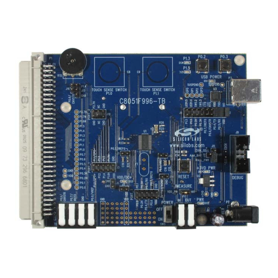
Figure 1. C8051F996 Target Board
Copyright © 2014 by Silicon Laboratories
C 8 0 5 1 F 9 9 x
K
U
'
G
I T
SER
S
UIDE
C8051F99x
Advertisement

Subscribe to Our Youtube Channel
Related Manuals for Silicon Laboratories C8051F99 Series


Summary of Contents for Silicon Laboratories C8051F99 Series
- Page 1 Third Party Tools CD AC to DC Power Adapter USB Debug Adapter (USB to Debug Interface) 2 USB Cables 2 AAA Batteries CD-ROM Figure 1. C8051F996 Target Board Rev. 0.2 2/14 Copyright © 2014 by Silicon Laboratories C8051F99x...
-
Page 2: Hardware Setup
C8051F99x 3. Hardware Setup Refer to Figure 2 for a diagram of the hardware configuration. 1. Connect the USB Debug Adapter to the DEBUG connector on the target board with the 10-pin ribbon cable. 2. Connect one end of the USB cable to the USB connector on the USB Debug Adapter. 3. -
Page 3: Software Setup
C8051F99x 4. Software Setup Simplicity Studio greatly reduces development time and complexity with Silicon Labs EFM32 and 8051 MCU products by providing a high-powered IDE, tools for hardware configuration, and links to helpful resources, all in one place. Once Simplicity Studio is installed, the application itself can be used to install additional software and documentation components to aid in the development and evaluation process. - Page 4 C8051F99x 4.1. Running Blinky Each project has its own source files, target configuration, SDK configuration, and build configurations such as the Debug and Release build configurations. The IDE can be used to manage multiple projects in a collection called a workspace.
- Page 5 C8051F99x 4.3. Legacy 8-bit IDE Note: Using the Simplicity Studio tools with the C8051F996 Development Kit is recommended. See section 4. "Software Setup‚" on page 3 for more information. Download the 8-bit software from the website (www.silabs.com/8bit-software) or use the provided installer on the CD-ROM to install the software tools for the C8051F99x devices.
- Page 6 C8051F99x 4. Click on the Get LIC via Internet... button to open the Obtaining a License IDE Code (LIC) window. 5. Press OK to open a browser window to the Keil website. If the window doesn’t open, navigate to www.keil.com/license/install.htm. 6.
- Page 7 C8051F99x 4.5. Silicon Labs Battery Life Estimator The Battery Life Estimator is a system design tool for battery operated devices. It allows the user to select the type of battery they are using in the system and enter the supply current profile of their application. Using this information, it performs a simulation and provides an estimated system operating time.
- Page 8 C8051F99x Figure 6. Battery Life Estimator Discharge Profile Editor The Discharge Profile Editor allows the user to modify the profile name and description. The four text entry boxes on the left hand side of the form allow the user to specify the amount of time the system spends in each power mode.
- Page 9 C8051F99x The wakeup frequency box calculates the period of a single iteration through the four power modes and displays the system wake up frequency. This is typically the "sample rate" in low power analog sensors. Once the battery type and discharge profile is specified, the user can click the "Simulate" button to start a new simulation.
-
Page 10: Target Board
C8051F99x 5. Target Board The C8051F996 Development Kit includes a target board with a C8051F996 device pre-installed for evaluation and preliminary software development. Numerous input/output (I/O) connections are provided to facilitate prototyping using the target board. Refer to Figure 8 for the locations of the various I/O connectors. Figure 10 on page 12 shows the factory default shorting block positions. - Page 11 C8051F99x The following items are located on the bottom side of the board. See Figure 9. BH1 Battery Holder for 1.5 V AAA. BH2 Battery Holder for 1.5 V AAA. BH3 Battery Holder for 3 V Coin Cell (CR2032). (CR2032) (AAA) (AAA) Figure 9.
- Page 12 C8051F99x 5.1. Target Board Shorting Blocks: Factory Defaults The C8051F996 Target Board comes from the factory with pre-installed shorting blocks on many headers. Figure 10 shows the positions of the factory default shorting blocks. P1.3 P0.2 P0.3 P1.5 P1.4 USB POWER TOUCH SENSE SWITCH TOUCH SENSE SWITCH P1.0...
- Page 13 C8051F99x 5.2. Target Board Power Options and Current Measurement (J10, J11, J17, H2, P2, P3, SW5) The C8051F996 Target Board supports three power options, selectable by the three-way header (J10/J11). Power to the MCU may be switched on/off using the power switch (SW5). The power options are described in the paragraphs below.
- Page 14 C8051F99x 5.3. System Clock Sources 5.3.1. Internal Oscillators The C8051F996 device installed on the target board features a factory calibrated programmable high-frequency internal oscillator (24.5 MHz base frequency, ±2%) and a low power internal oscillator (20 MHz ±10%). After each reset, the low power oscillator divided by 8 results in a default system clock frequency of 2.5 MHz (±10%).
- Page 15 C8051F99x 5.5. Switches and LEDs (J1, J5, J8, J15, J16, SW1, SW2, SW3) Three push-button switches are provided on the target board. Switch SW1 (RESET) is connected to the reset pin of the C8051F996. Pressing SW1 puts the device into its hardware-reset state. Switches SW2 (P0.2) and SW3 (P0.3) are connected to the C8051F996’s general purpose I/O (GPIO) pins through headers.
- Page 16 C8051F99x 5.6. Expansion I/O Connector (P1) The 96-pin Expansion I/O connector P1 provides access to all signal pins of the C8051F996 device (except the C2 debug interface signals). In addition, power supply and ground pins are included. A small through-hole prototyping area is also provided.
- Page 17 C8051F99x 5.7. Target Board DEBUG Interface (J9) The DEBUG connector J9 provides access to the DEBUG (C2) pins of the C8051F996. It is used to connect the USB Debug Adapter to the target board for in-circuit debugging and Flash programming. Table 3 shows the DEBUG pin definitions.
- Page 18 C8051F99x 5.10. IREF Connector (J7) The C8051F996 Target Board also features a current-to-voltage 1 k load resistor that may be connected to the current reference (IREF0) output that can be enabled on port pin (P0.7). Install a shorting block on J7 to connect port pin P0.7 of the target device to the load resistor.
- Page 19 C8051F99x 6. Schematics Rev. 0.2...
- Page 20 C8051F99x Rev. 0.2...
- Page 21 C8051F99x Rev. 0.2...
- Page 22 C8051F99x OTES Rev. 0.2...
-
Page 23: Contact Information
Silicon Laboratories products are not designed, intended, or authorized for use in applications intended to support or sustain life, or for any other application in which the failure of the Silicon Laboratories product could create a situation where per- sonal injury or death may occur.
Need help?
Do you have a question about the C8051F99 Series and is the answer not in the manual?
Questions and answers