Advertisement
Quick Links
C8051F930 D
1. Relevant Devices
The C8051F930 Development Kit is intended as a development platform for the microcontrollers in the
C8051F93x-C8051F92x MCU family. The members of this MCU family are C8051F930, C8051F931, C8051F920,
and C8051F921.
Notes:
1. The target board included in this kit is provided with a pre-soldered C8051F930 MCU (LQFP32 package).
2. Code developed on the C8051F930 can be easily ported to the other members of this MCU family.
3. Refer to the C8051F93x-C8051F92x data sheet for the differences between the members of this MCU family.
2. Kit Contents
The C8051F930 Development Kit contains the following items:
C8051F930 Target Board
C8051Fxxx Development Kit Quick-Start Guide
Silicon Laboratories IDE and Product Information CD-ROM. CD content includes the following:
Silicon Laboratories Integrated Development Environment (IDE)
Keil 8051 Development Tools (macro assembler, linker, evaluation C compiler)
Source code examples and register definition files
Documentation
C8051F930 Development Kit User's Guide (this document)
AC to DC Power Adapter
USB Debug Adapter (USB to Debug Interface)
2 USB Cables
2 AAA Batteries
Rev. 0.5 8/09
Downloaded from
Elcodis.com
electronic components distributor
K
EVELOPMENT
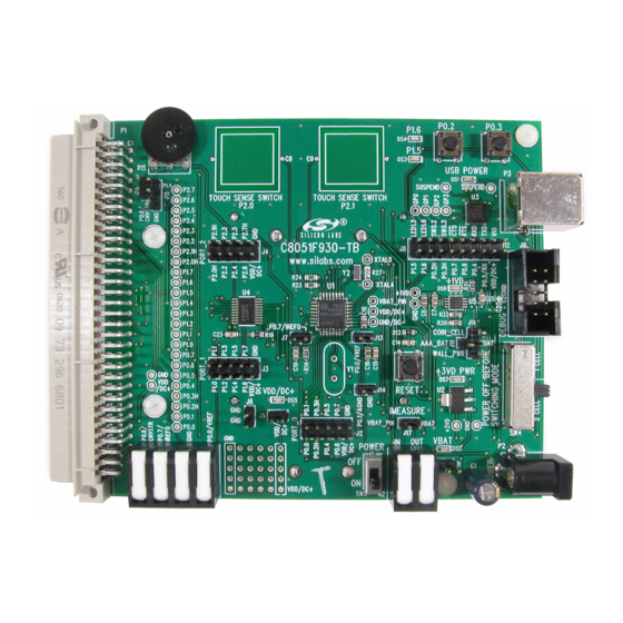
Figure 1. C8051F930 Target Board
Copyright © 2009 by Silicon Laboratories
C 8 0 5 1 F 9 3 0 - D K
U
'
G
IT
S E R
S
UIDE
C8051F930-DK
Advertisement

Related Manuals for Silicon Laboratories C8051F930-DK


Summary of Contents for Silicon Laboratories C8051F930-DK
- Page 1 C8051F930 Target Board C8051Fxxx Development Kit Quick-Start Guide Silicon Laboratories IDE and Product Information CD-ROM. CD content includes the following: Silicon Laboratories Integrated Development Environment (IDE) Keil 8051 Development Tools (macro assembler, linker, evaluation C compiler) ...
- Page 2 The Silicon Laboratories IDE integrates a source-code editor, a source-level debugger, and an in-system Flash programmer. See Section 5. "Using the Keil Software 8051 Tools with the Silicon Laboratories IDE‚" on page 9 for detailed information on how to use the IDE. The Keil Evaluation Toolset includes a compiler, linker, and assembler and easily integrates into the IDE.
- Page 3 C8051F930-DK 3.3.2. 3rd Party Toolsets The Silicon Laboratories IDE has native support for many 8051 compilers. The full list of natively supported tools is as follows: Keil Raisonance Tasking Hi-Tech SDCC The demo applications for the C8051F930 target board are written to work with the Keil and SDCC toolsets.
- Page 4 C8051F930-DK 3.5. Configuration Wizard 2 The Configuration Wizard 2 is a code generation tool for all of the Silicon Laboratories devices. Code is generated through the use of dialog boxes for each of the device's peripherals. Figure 2. Configuration Wizard 2 Utility The Configuration Wizard utility helps accelerate development by automatically generating initialization source code to configure and enable the on-chip resources needed by most design projects.
- Page 5 C8051F930-DK 3.6. Silicon Labs Battery Life Estimator The Battery Life Estimator is a system design tool for battery operated devices. It allows the user to select the type of battery they are using in the system and enter the supply current profile of their application. Using this information, it performs a simulation and provides an estimated system operating time.
- Page 6 C8051F930-DK Figure 4. Battery Life Estimator Discharge Profile Editor The Discharge Profile Editor allows the user to modify the profile name and description. The four text entry boxes on the left hand side of the form allow the user to specify the amount of time the system spends in each power mode.
- Page 7 C8051F930-DK The wakeup frequency box calculates the period of a single iteration through the four power modes and displays the system wake up frequency. This is typically the "sample rate" in low power analog sensors. Once the battery type and discharge profile is specified, the user can click the "Simulate" button to start a new simulation.
- Page 8 4. Hardware Setup using a USB Debug Adapter The target board is connected to a PC running the Silicon Laboratories IDE via the USB Debug Adapter as shown in Figure 6. 1. Connect the USB Debug Adapter to the DEBUG connector on the target board with the 10-pin ribbon cable.
- Page 9 Keil 8051 tools with the Silicon Laboratories IDE. To build an absolute object file using the Silicon Laboratories IDE project manager, you must first create a project. A project consists of a set of files, IDE configuration, debug views, and a target build configuration (list of files and tool configurations used as input to the assembler, compiler, and linker when building an output object file).
- Page 10 C8051F930-DK 5.2. Building and Downloading the Program for Debugging 1. Once all source files have been added to the target build, build the project by clicking on the Build/Make Project button in the toolbar or selecting Project Build/Make Project from the menu.
- Page 11 C8051F930-DK 6. Example Source Code Example source code and register definition files are provided in the “SiLabs\MCU\Examples\C8051F93x_92x\” default directory during IDE installation. These files may be used as a template for code development. Example applications include a blinking LED example which configures the green LED on the target board to blink at a fixed rate.
- Page 12 C8051F930-DK 7. Target Board The C8051F930 Development Kit includes a target board with a C8051F930 device pre-installed for evaluation and preliminary software development. Numerous input/output (I/O) connections are provided to facilitate prototyping using the target board. Refer to Figure 7 for the locations of the various I/O connectors. Figure 9 on page 14 shows the factory default shorting block positions.
- Page 13 C8051F930-DK The following items are located on the bottom side of the board. See Figure 8. Battery Holder for 1.5 V AAA. Use for one-cell or two-cell mode. Battery Holder for 1.5 V AAA. Use for two-cell mode only. Battery Holder for 3 V Coin Cell (CR2032).
- Page 14 C8051F930-DK 7.1. Target Board Shorting Blocks: Factory Defaults The C8051F930 target board comes from the factory with pre-installed shorting blocks on many headers. Figure 9 shows the positions of the factory default shorting blocks. P1.6 P0.2 P0.3 P1.5 P1.4 USB POWER...
- Page 15 C8051F930-DK 7.2. Target Board Power Options and Current Measurement The C8051F930 Target Board supports three power options, selectable by the three-way header (J10/J11). The power options vary based on the configuration (one-cell or two-cell mode) selected by SW4. Power to the MCU may be switched on/off using the power switch (SW5).
- Page 16 C8051F930-DK 7.3. System Clock Sources 7.3.1. Internal Oscillators The C8051F930 device installed on the target board features a factory calibrated programmable high-frequency internal oscillator (24.5 MHz base frequency, ±2%) and a low power internal oscillator (20 MHz ±10%). After each reset, the low power oscillator divided by 8 results in a default system clock frequency of 2.5 MHz (±10%).
- Page 17 C8051F930-DK 7.5. Switches and LEDs Three push-button switches are provided on the target board. Switch SW1 is connected to the reset pin of the C8051F930. Pressing SW1 puts the device into its hardware-reset state. Switches SW2 and SW3 are connected to the C8051F930’s general purpose I/O (GPIO) pins through headers.
- Page 18 C8051F930-DK 7.6. Expansion I/O Connector (P1) The 96-pin Expansion I/O connector P1 provides access to all signal pins of the C8051F930 device (except the C2 debug interface signals). In addition, power supply and ground pins are included. A small through-hole prototyping area is also provided.
- Page 19 C8051F930-DK 7.7. Target Board DEBUG Interface (J9) The DEBUG connector J9 provides access to the DEBUG (C2) pins of the C8051F930. It is used to connect the Serial Adapter or the USB Debug Adapter to the target board for in-circuit debugging and Flash programming.
- Page 20 C8051F930-DK 7.10. IREF Connector (J7) The C8051F930 Target Board also features a current-to-voltage 1 k load resistor that may be connected to the current reference (IREF0) output that can be enabled on port pin (P0.7). Install a shorting block on J7 to connect port pin P0.7 of the target device to the load resistor.
- Page 21 4. Where can I find a schematic of the C8051F930 Target Board? A target board schematic can be found in the C8051F930-DK User’s Guide which is available on the Development Tools CD and is installed in the following folder (by default): C:\SiLabs\MCU\Documentation\UsersGuides 5.
- Page 22 C8051F930-DK 6. What can I do to reduce active supply current? Below are some suggestions for reducing the active supply current: a. Clear all wake-up sources in the PCU0CF register. This will allow the low power oscillator to be disabled when it is not being used as the system clock.
- Page 23 C8051F930-DK 11. When the missing clock detector is enabled, why does the MCU reset if I switch from the default system clock (Low Power Oscillator divided by 8) to smaRTClock divided by 1? Background: —The missing clock detector will trigger a reset if the system clock period exceeds 100 µs.
- Page 24 C8051F930-DK 9. Schematics Rev. 0.5 Downloaded from Elcodis.com electronic components distributor...
- Page 25 C8051F930-DK Rev. 0.5 Downloaded from Elcodis.com electronic components distributor...
- Page 26 C8051F930-DK Rev. 0.5 Downloaded from Elcodis.com electronic components distributor...
- Page 27 C8051F930-DK OTES Rev. 0.5 Downloaded from Elcodis.com electronic components distributor...
- Page 28 Silicon Laboratories products are not designed, intended, or authorized for use in applications intended to support or sustain life, or for any other application in which the failure of the Silicon Laboratories product could create a situation where per- sonal injury or death may occur.
Need help?
Do you have a question about the C8051F930-DK and is the answer not in the manual?
Questions and answers