
Related Manuals for GE IPN250RTM


Summary of Contents for GE IPN250RTM
- Page 1 Intelligent Platforms Hardware Reference Manual IPN250RTM Edition 2 Publication No. IPN250RTM-HRM/2...
- Page 2 Errata to Section 2.1 and Table 2-3 February 2011 Board Artwork Rev 2 2 + errata February 2011 Errata to Section 2.2 and Table 2-12 Waste Electrical and Electronic Equipment (WEEE) Returns GE Intelligent Platforms Limited is registered with an approved Producer Compliance Scheme (PCS) and, subject to suitable contractual arrangements being in place, will ensure WEEE is processed in accordance with the requirements of the WEEE Directive. GE Intelligent Platforms Limited. will evaluate requests to take back products purchased by our customers before August 13, 2005 on a case by case basis. A WEEE management fee may apply. Publication No. IPN250RTM-HRM/2...
- Page 3 Links take you to other documents or websites. The purple link color may also be used within a body of text or paragraph to indicate a link (or hyperlink) to a different part of the same document . Publication No. IPN250RTM-HRM/2 About This Manual 3...
- Page 4 VPX I/O Modules Hardware Reference Manual, publication number VPXIOM-0HH. GE Websites Information regarding all GE Intelligent Platforms products can be found on the following website: LINK http://www.ge-ip.com/products/family/embedded-systems. Third Party Manuals ANSI/VITA 46.0‐2007 VPX Baseline Standard. VITA 65 OpenVPX System Specification Rev 1.04 Jan 1 2010. These are the latest versions at time of writing; check web sites for later updates. NOTE Registration may be required for access to some of these documents. Third Party Web Sites LINK http://www.vita.com/vso for standards. 4 IPN250RTM Publication No. IPN250RTM-HRM/2...
- Page 5 Technical Support Technical assistance contact details can be found on the web site Support Locator page. The appropriate product category is headed ʺDSP, SBCs, Multiprocessors and Graphics (formerly Radstone)ʺ LINK http://www.ge-ip.com/support/embeddedsupport/locator. Queries will be logged on the Technical Support database and allocated a unique Service Request (SR) number for use in future correspondence. Alternatively, you may also contact GE Intelligent Platformsʹ Technical Support via: LINK support .towcester.ip@ge.com. TELEPHONE +44 (0) 1327 322760 Returns If you need to return a product, there is a Return Materials Authorization (RMA) request form that can be printed out and filled in, available via the web site Repairs page. LINK http://www.ge-ip.com/support/embeddedsupport/rmalocator. RMA Request Form (Word Doc)” hyperlink under “DSP, Follow the “Download SBCs, Multiprocessors and Graphics (Formerly Radstone)”. Do not return products without first contacting the factory. Publication No. IPN250RTM-HRM/2 About This Manual 5...
-
Page 6: Table Of Contents
2.3.4 IPN250RTM Interface Connector (J10) ........ - Page 7 3.2.3 Power Good LED (DS34) ..............29 Publication No. IPN250RTM-HRM/2...
-
Page 8: Ipn250Rtm
1 • IPN250RTM 1.1 Functional Description The IPN250RTM is the payload Rear Transition Module (RTM) for the IPN250 Single Board Computer. The IPN250RTM provides access to the P3 to P6 rear I/O functions of the IPN250 via connector styles commonly used throughout the industry. The IPN250RTM can be used with the GEIP OVPX64UBP backplane, the IPN250 and the FABRTMP1 to produce a fully configured system. The IPN250RTM can also be used with the IPN250 with other backplanes that provide the fabric connections ‘wired’ into the backplane. The OVPX64UBP backplane functionality is described in the SCVPX6U development chassis manual. LINK SCVPX6U Hardware Reference Manual, publication number SCVPX6U-HRM. 1.2 Fitting RTMs See the VPX I/O Modules manual for fitting instructions. LINK VPX I/O Modules Hardware Reference Manual, publication number VPXIOM-0HH. 1.3 Current Requirements The IPN250RTM draws a maximum of 180 mA from the VPX 3.3V‐AUX supply ... -
Page 9: Layout
The assembly will not fit within the height profile of a single VPX backplane slot, and will encroach into the area normally reserved for the RTM of the adjacent slot. If the 1.6 inch pitch IPN250RTM-111 assembly does not suit your requirements for a deployed system that uses RTMs, contact GEIP Product Management to discuss alternatives. - Page 10 Figure 1-2 IPN250RTMB 10 IPN250RTM Publication No. IPN250RTM-HRM/2...
- Page 11 Figure 1-3 IPN250RTMA and IPN250RTMB Assembly Publication No. IPN250RTM-HRM/2 IPN250RTM 11...
-
Page 12: Openvpx Slot Profile
1.7 OpenVPX Slot Profile The IPN250RTM supports the SLT6‐PAY‐4F1Q2UT2T‐10.2.1 OpenVPX Payload Slot Profile with the following non‐fabric connectivity: • P0/J0 is used by the Utility plane • P3/J3 is user defined • P4/J4 is partly used by the Control planes. The remainder of P4/J4 and the single ended signals are all user defined – A Control plane of two ultra‐thin pipes – A Control plane of two thin pipes. • P5/J5 is user defined • P6/J6 is user defined 12 IPN250RTM Publication No. IPN250RTM-HRM/2... -
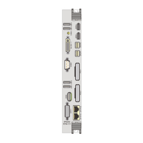
Page 13: Connectors
USB interface x-IPN250RTMA IPN250RTM interface x-IPN250RTMA GPIO header x-IPN250RTMA JTAG header x-IPN250RTMA Spare header x-IPN250RTMA P3V3 header x-IPN250RTMA Dediprog interface x-IPN250RTMB J4, J5, J6 TV capture x-IPN250RTMB IPN250RTM interface x-IPN250RTMB Audio header x-IPN250RTMB Serial COM2 interface Publication No. IPN250RTM-HRM/2 Connectors 13... -
Page 14: Dvi/Hdmi Selection
OpenVPX Payload Slot Profile SLT6‐PAY‐4F1Q2UT2T‐10.2.1. These pipes are brought out to a dual (side by side) RJ45‐type connector, pinned out to the TIA/EIA 568 standard. Table 2-2 IPN250RTMA J3 Connector Pin Assignments Pin (A) Signal Pin (B) Signal CPTP01_DAP CPTP02_DAP CPTP01_DAN CPTP02_DAN CPTP01_DBP CPTP02_DBP CPTP01_DCP CPTP02_DCP CPTP01_DCN CPTP02_DCN CPTP01_DBN CPTP02_DBN CPTP01_DDP CPTP02_DDP CPTP01_DDN CPTP02_DDN The signal pairs are 100 differential and matched. GEIP offers cable C‐CBL000122‐001, which is a 2m long Cat5E Ethernet patch cable with RJ45 connectors. 14 IPN250RTM Publication No. IPN250RTM-HRM/2... -
Page 15: 1000Basekx Ethernet Channels 1 And 2 Connectors (J4 & J5)
2.3.3 PCI Express Interface Connectors (J6, J7) User‐defined connections include 4 differential pairs of PCIe. These are connected as two ports of 1‐lane PCIe on the IPN250RTM. NOTE The PCIe differential pairs can only be used as two 1-lane ports; they cannot be used together to form a single 2-lane PCIe port. J6 and J7 provide the PCIe interfaces via two Molex 75586‐0007 PCI Express Cabling Standard 8‐lane PCIe cable connectors. On both connectors, only the first lane is populated; the other lanes have their positive/negative pairs connected together via 100 terminating resistors, in accordance with the PCIe cabling standard. J6 provides lane 1 and J7 provides lane 2. All power and management signals are unused, and have been grounded via 100 resistors to maximize the noise immunity of the cable. Publication No. IPN250RTM-HRM/2 Connectors 15... - Page 16 NOTE The IPN250 supports three x1 lane PCIe ports. However, there is insufficient space on the IPN250RTM front panel to bring all three PCIe ports to connectors. Table 2-4 IPN250RTMA J6 Pin Assignments Side B Side A Connector IPN250RTM Connector...
- Page 17 100R link to B30 PERN6 100R link to B29 PETN6 100R link to B29 PERP7 100R link to B33 PETP7 100R link to A33 PERN7 100R link to B32 PETN7 100R link to A32 GEIP offers cable C‐ASY000286‐801, which is a 0.5m long PCIe cable with Molex 74546‐0813 connectors. Publication No. IPN250RTM-HRM/2 Connectors 17...
-
Page 18: Ipn250Rtm Interface Connector (J10)
2.3.4 IPN250RTM Interface Connector (J10) This header connects to P1 on the IPN250RTMB. 2.3.5 GPIO Header (P1) Table 2-6 IPN250RTMA P1 Header Pin Assignments Signal Signal GPIO_0 GPIO_1 GPIO_2 GPIO_3 GPIO_4 GPIO_5 GPIO_6 GPIO_7 2.3.6 JTAG Header (P2) This brings out the JTAG signals on the IPN250. Table 2-7 IPN250RTMA P2 Header Pin Assignments Signal... -
Page 19: Spare Signals Header (P3)
2.3.8 P3V3 Header (P4) This header is provided for convenience in using the Lattice programmer with the JTAG Header (P2). All pins on P4 are connected to P3V3_AUX so that the Lattice programmer can use any of them. Table 2-9 IPN250RTMA P4 Header Pin Assignments Signal Signal P3V3_AUX P3V3_AUX P3V3_AUX P3V3_AUX P3V3_AUX P3V3_AUX P3V3_AUX P3V3_AUX 2.3.9 Dediprog Interface Header (P5) CAUTION This header is now a no-fit option. Publication No. IPN250RTM-HRM/2 Connectors 19... -
Page 20: Sata0/1 Connectors (P9/ P10)
2.3.10 SATA0/1 Connectors (P9/ P10) Table 2-10 IPN250RTMA P9, P10 Connector Pin Assignments P9 Pin Signal P10 Pin Signal SATA0_TXP SATA1_TXP SATA0_TXN SATA1_TXN SATA0_RXN SATA1_RXN SATA0_RXP SATA1_RXP The signal pairs are 100 differential. GEIP offers cable C‐CBL000155‐001, which is a 0.6m long SATA cable. 20 IPN250RTM Publication No. IPN250RTM-HRM/2... -
Page 21: Ipn250Rtmb
HDMI_DVI_CLKP HDMI_DVI_CLKN Unconnected DDC2_CLOCK DDC2_DATA Unconnected DDC2_5V HOTPLUG2 NOTE This connector is not available for use on the Rev 1 IPN250RTM. 2.4.2 TV Capture Connectors (J3 to J6) The IPN250 supports capture of video from up to four TV‐format video sources. These can be connected to four SSMB connectors on the IPN250RTM. J3 is accessible via the front panel of the IPN250RTM, and can be used for testing basic operation of the TV capture device. J4 to J6 are fitted in‐board and are most likely to be used during design validation of the IPN250. The SSMB connectors route the TV signals as follows: Table 2-12 TV Capture Connectors Connector... -
Page 22: Multi-Display Connector (J7)
GMCH_GREEN GMCH_DVI_TX0N GMCH_DVI_CLKN Quiet GND Quiet GND GMCH_DVI_TX0P GMCH_DVI_CLKP a. Not currentlu used. b. Fused at 500 mA. Figure 2-2 Pin Numbering on J7 An adaptor cable is required to convert the J7 pinout to conventional DVI‐I connectors. GEIP offers a StarTech DMSDVIDVI multi‐display cable, which is an 8 inch long DMS 59‐way male to dual DVI‐I female adaptor cable, as shown below: Figure 2-3 Dual VGA/DVI Cable If analog VGA RGB only is required, a suitable Multi‐Display to VGA adaptor can be used. 22 IPN250RTM Publication No. IPN250RTM-HRM/2... -
Page 23: Gpu Dvi-Dual Link Connector (J8)
J9 Pin Signal P5V_USBP0 P5V_USBP1 USB0_DN USB1_DN USB0_DP USB1_DP The signal pairs are 90 differential. 2.4.6 USB2/3 Connectors (J11/ J12) Table 2-1 IPN250RTMA J11, J12 Connector Pin Assignments J11 Pin Signal J12 Pin Signal P5V_USBP2 P5V_USBP3 USB2_DN USB3_DN USB2_DP USB3_DP The signal pairs are 90 differential. Publication No. IPN250RTM-HRM/2 Connectors 23... -
Page 24: Ipn250Rtm Interface Connector (P1)
2.4.7 IPN250RTM Interface Connector (P1) This socket connects to J10 on the IPN250RTMA. 2.4.8 COM1 Connector (P3) The IPN250 supports front or rear COM port connection, but only one set of connectors can be active at a time. The IPN250RTM provides rear connection via a standard 9‐way sub‐miniature male D‐type connector P3 and also via a 2x5 way header on the PCB P5 (see Section 2.4.10 ʺCOM2 Connector (P5)ʺ). The following table gives RS232 and RS422/485 versions of the available signals. Table 2-2 IPN250RTMB P3 Pin Assignments Signal Signal Interconnect Interconnect COM1_RXD_RXN COM1_RTS_TXP COM1_TXD_TXN COM1_CTS_RXP Interconnect Unconnected a. Pins 1, 4 and 6 are connected together. -
Page 25: Com2 Connector (P5)
LINK See also Section 2.4.8 "COM1 Connector (P3)" The following table gives RS232 and RS422/485 versions of the available signals. Table 2-4 IPN250RTMB P5 Pin Assignments Signal Signal Unconnected Interconnect COM2_RXD_RXN COM2_CTS_RXP COM2_TXD_TXN COM2_RTS_TXP Interconnect Interconnect Unconnected a. Pins 1, 7, and 8 are connected together. Publication No. IPN250RTM-HRM/2 Connectors 25... -
Page 26: Switches And Leds
CAUTION Only set System Controller on one of the backplane, the IPN250RTM or the FABRTMP1 (more than one may result in the incorrect payload board or multiple payload boards being set as System Controller). Whichever is not used should have DIP switches/links set/left open. -
Page 27: Pcie Switch Configuration
NVMRO CAUTION If NVMRO is to be set elsewhere instead of on the IPN250RTM, ensure that the DIP switch/link is set/left open. 3.1.2 PCIe Switch Configuration LINK Refer to Figure 1-1 for the location of the P8 switch bank. The IPN250 includes a PCIe switch, some basic configuration of which can be ... -
Page 28: Leds
May not reflect the setting of the corresponding DIP switch on the IPN250RTM if non-volatile memory has been write-enabled elsewhere in the system. b.May not reflect the setting of the corresponding DIP switch on the IPN250RTM if the associated IPN250 has been made System Controller via the backplane or FABRTMP1. - Page 29 3.2.3 Power Good LED (DS34) The device used for selecting between the HDMI and DVI outputs on the IPN250RTM requires a local 3.3V supply. An on‐board regulator produces this voltage from the P5V supply. This red ‘power good’ LED shows when this power supply is operational. CAUTION Do not assume that this LED shows that the power supply is within a specific voltage tolerance. Publication No. IPN250RTM-HRM/2 Switches and LEDs 29...
- Page 30 1 800 322 3616 or 1 256 880 0444 Confidential Information - This document contains Confidential/Proprietary Information www.ge-ip.com of GE Intelligent Platforms, Inc. and/or its Asia Pacific: suppliers or vendors. Distribution or 86 10 6561 1561 reproduction prohibited without permission.
Need help?
Do you have a question about the IPN250RTM and is the answer not in the manual?
Questions and answers