
Related Manuals for Innodisk nanoSSD PCIe 3TE7 Series


Summary of Contents for Innodisk nanoSSD PCIe 3TE7 Series
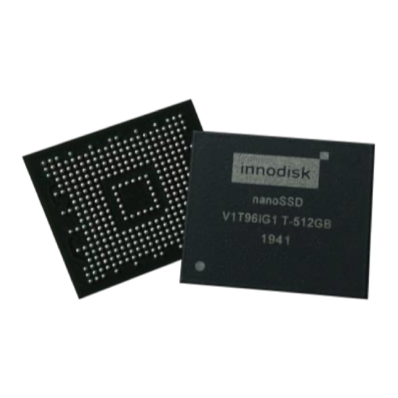
- Page 1 PCIe 3TE7 Series Customer: Customer Part Number: Innodisk Part Number: Innodisk Model Name: Date: Innodisk Customer Approver Approver...
-
Page 2: Table Of Contents
nanoSSD PCIe 3TE7 Table fo contents LIST OF FIGURES ......................7 1. PRODUCT OVERVIEW ....................8 1.1 I SSD PCI 3TE7 ............. 8 NTRODUCTION OF NNODISK NANO 1.2 P ..................8 RODUCT IEW AND ODELS 2. PRODUCT SPECIFICATIONS ..................9 2.1 Capacity and Device Parameters ................ - Page 3 nanoSSD PCIe 3TE7 4.2.2 Reflow Profile ..................... 21 5. PART NUMBER RULE ....................23 Rev 1.7 TPS, Apr., 2022...
- Page 4 nanoSSD PCIe 3TE7 EVISION ISTORY Revision Description Date Rev. 1.0 First Released Sep., 2020 Rev. 1.1 Update MSL Declaration Oct., 2020 Rev. 1.2 Update 512GB Nov., 2020 Rev. 1.3 Remove AES and TCG Opal support Jun., 2021 Rev. 1.4 Updates: Jul., 2021 - pin layout drawing - pin assignment for Y19...
- Page 5 Sequential Write up to 1,350 MB/s DWPD 32GB 0.81 64GB 0.81 128GB 0.81 256GB 0.81 512GB 0.81 Data Retention Years Warranty 2 Years* *2years duration after 100% (3000) P/E cycles at 55℃ For warranty details, please refer to: https://www.innodisk.com/en/support_and_service/warranty Rev 1.7 TPS, Apr., 2022...
- Page 6 nanoSSD PCIe 3TE7 List of Tables 1: D ABLE EVICE PARAMETERS ............................. 9 2: P ABLE ERFORMANCE ..............................9 3: I SSD PCI 3TE7 P ABLE NNODISK NANO OWER EQUIREMENT ..............10 4: P ABLE OWER ONSUMPTION ..........................10 5: T SSD PCI 3TE7 ................
-
Page 7: List Of Figures
nanoSSD PCIe 3TE7 List of Figures 1: I SSD PCI 3TE7 ......................8 IGURE NNODISK NANO 2: I SSD PCI 3TE7 P IGURE NNODISK NANO AYOUT ................16 3: I SSD PCI 3TE7 B IGURE NNODISK NANO LOCK IAGRAM ................ 19 Rev 1.7 TPS, Apr., 2022... -
Page 8: Product Overview
TRIM enables SSD’s controller to skip invalid data instead of moving. It can free up significant amount of resources, extends the lifespan of SSD by reducing erase, and write cycles on the SSD. Innodisk’s handling of garbage collection along with TRIM command improves write performance on SSDs. -
Page 9: Product Specifications
nanoSSD PCIe 3TE7 2. Product Specifications 2.1 Capacity and Device Parameters nanoSSD PCIe 3TE7 device parameters are shown in Table 1. Table 1: Device parameters User Capacity Capacity (MB) 32GB 62533296 30533 64GB 125045424 61057 128GB 250069680 122104 256GB 500118192 244198 512GB 1000215216... -
Page 10: Electrical Specifications
PCIe 3TE7 2.3 Electrical Specifications 2.3.1 Power Requirement Table 3: Innodisk nanoSSD PCIe 3TE7 Power Requirement Item Symbol Rating Unit Input voltage +3.3 DC +- 5% 2.3.2 Power Consumption Table 4: Power Consumption Voltage Rail Rating Power Consumption (W) Main power supply 3.3 V ±... -
Page 11: Humidity
Table 7: nanoSSD PCIe 3TE7 MTBF Product Condition MTBF (Hours) Innodisk nanoSSD PCIE 3TE7 Telcordia SR-332 GB, 25°C >3,000,000 2.5 RoHS Compliance nanoSSD PCIE 3TE7 is fully compliant with RoHS directive. -
Page 12: Reliability
nanoSSD PCIe 3TE7 2.6 Reliability Parameter Value Read Cycles Unlimited Read Cycles Flash endurance 3,000 P/E cycles Wear-Leveling Algorithm Support Bad Blocks Management Support DIE RAID Recovery Support Error Correct Code Support TBW* (Total Bytes Written) Capacity Client workload 32GB 18.75 64GB 37.5... -
Page 13: Ball And Signal Description
“P” and “N” in differential signals, e.g. PTXP1 and PTXN1, mean positive-end signal and negative-end signal. In signal names with “#”, e.g. PCLKREQ#, PRESET#, RESET# and JT_TRST#, the “#” means “active low”. Table 8: Innodisk nanoSSD PCIe 3TE7 Pin Assignment Signal Name Ball Number Pin Type *... - Page 14 nanoSSD PCIe 3TE7 Signal Name Ball Number Pin Type * Description General Purpose Input and Output 0 General Purpose Input and Output 1 General Purpose Input and Output 2 Debug GPIO General Purpose Input and Output 3 (1.8V) General Purpose Input and Output 4 / Signal output to drive an external transistor to GP4/LED_1# provide status indication via LED device...
- Page 15 nanoSSD PCIe 3TE7 Power (0.9V) LDO Output - Core Power T2, T18, T19, Power for PCIe/PLL/Digital Input and Output, Power (1.8V) U2, U18,U19 Power Supplier Used by ATE Signal Name Ball Number Pin Type * Description A1, A2, A3, A6, A9, A12, A15, A18, A19, A20, AA1, AA2, AA3, AA6, AA9, AA12, AA15, AA18, AA19, AA20, AB1, AB2, AB3, AB6, AB9, AB12, AB15, AB18, AB19, AB20, B1, B2, B3, B9, B12, B15, B19,...
- Page 16 PCIe 3TE7 Figure 2: Innodisk nanoSSD PCIe 3TE7 Pin Layout Rev 1.7 TPS, Apr., 2022...
-
Page 17: Power Supply & Sequence
nanoSSD PCIe 3TE7 2.9 Power Supply & Sequence Voltage Rail Specification 3.3V± 10% Input voltage VCCQ 1.8V ± 5% VDDI 1.2V ± 5% Rev 1.7 TPS, Apr., 2022... -
Page 18: Mechanical Dimensions
2.10 Mechanical Dimensions Bottom View (345-ball) 2.11 Seek Time Innodisk nanoSSD PCIe 3TE7 is not a magnetic rotating design. There is no seek or rotational latency required. 2.12 NAND Flash Memory Innodisk nanoSSD PCIe 3TE7 uses 3D TLC NAND flash memory, with 3,000 program & erase cycles, which is non-volatility, high reliability and high-speed memory storage. -
Page 19: Theory Of Operation
PCIe 3TE7 3. Theory of Operation 3.1 Overview Figure 2 shows the operation of Innodisk nanoSSD PCIe 3TE7 from the system level, including the major hardware blocks. Figure 3: Innodisk nanoSSD PCIe 3TE7 Block Diagram Innodisk nanoSSD PCIe 3TE7 integrates a PCIe Gen 3x2 controller and NAND flash memories. -
Page 20: Bad Blocks Management
3.5 Power Cycling Innodisk’s power cycling management is a comprehensive data protection mechanism that functions before and after a sudden power outage to SSD. Low-power detection terminates data writing before an abnormal power-off, while table-remapping after power-on deletes corrupt data and maintains data integrity. -
Page 21: Installation Requirements
nanoSSD PCIe 3TE7 4. Installation Requirements 4.1 Reference Design A reference design using the nanoSSD has been provided here to help with the integration. All peripheral circuits are included in the design and meet specifications laid out in the earlier sections of this document. - Page 22 nanoSSD PCIe 3TE7 Rev 1.7 TPS, Apr., 2022...
- Page 23 nanoSSD PCIe 3TE7 5. Part Number Rule CODE D E N S D - C 1 2 I nanoSSD Flash Operation Internal Customized Description Disk Capacity Category Flash PCIe 3TE7 Mode Temp. Control Code Definition Code 1 (Disk) Code 13 (Flash mode) D : Disk E: 64 layers 3D flash...
Need help?
Do you have a question about the nanoSSD PCIe 3TE7 Series and is the answer not in the manual?
Questions and answers