Advertisement
Quick Links
e
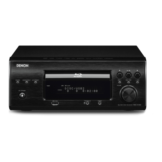
RBD-X1000
• For purposes of improvement, specifications and design are subject to change without notice.
• Please use this service manual with referring to the operating instructions without fail.
• Some illustrations using in this service manual are slightly different from the actual set.
S0419-0V07DM/DG1112
SERVICE MANUAL
MODEL
BLU-RAY DISC/DVD SURROUND RECEIVER
Copyright 2011 D&M Holdings Inc. All rights reserved.
WARNING: Violators will be prosecuted to the maximum extent possible.
JP
E3
E2
P
e
D&M Holdings Inc.
Ver. 7
Please refer to the
MODIFICATION NOTICE.
EK
K2A E1C E1K EUT
Advertisement

Related Manuals for Denon RBD-X1000


Summary of Contents for Denon RBD-X1000
- Page 1 MODIFICATION NOTICE. SERVICE MANUAL MODEL K2A E1C E1K EUT RBD-X1000 BLU-RAY DISC/DVD SURROUND RECEIVER • For purposes of improvement, specifications and design are subject to change without notice. • Please use this service manual with referring to the operating instructions without fail.
- Page 2 SAFETY PRECAUTIONS The following check should be performed for the continued protection of the customer and service technician. LEAKAGE CURRENT CHECK Before returning the unit to the customer, make sure you make either (1) a leakage current check or (2) a line to chassis resistance check.
- Page 3 NOTE FOR SCHEMATIC DIAGRAM WARNING: Parts marked with this symbol z have critical characteristics. Use ONLY replacement parts recommended by the manufacture CAUTION: Before returning the unit to the customer, make sure you make either (1) a leakage current check or (2) a line to chassis resistance check. If the leakage current exceeds 0.5 milliamps, or if the resistance from chassis to either side of the power cord is less than 460 kohms, the unit is defective.
- Page 4 WARNING AND LASER SAFETY INSTRUCTIONS WARNING WAARSCHUWING Alle IC’s en vele andere halfgeleiders zijn gevoelig All ICs and many other semi-conductors are voor elektrostatische ontladingen (ESD). susceptible to electrostatic discharges (ESD). Onzorgvuldig behandelen tijdens reparatie kan de Careless handling during repair can reduce life levensduur drastisch doen verminderen.
- Page 5 TECHNICAL SPECIFICATIONS n Audio Section n Applicable Discs • Power amplifier BD-VIdeo discs : 12 cm 1 side 1 layer, 12 cm 1 side 2 layers Rated output : 70 W + 70 W (20 kHz, 6 Ω T.H.D. 10 %) DVD-VIdeo discs : 12 cm 1 side 1 layer, 12 cm 1 side 2 layers/ Output connectors : 6 – 16 Ω 12 cm 2 sides 2 layers (1 side 1 layer) • Analog 8 cm 1 side 1 layer, 8 cm 1 side 2 layers/ Input sensitivity/Input impedance : 200 mV/47 kΩ 8 cm 2 side 2 layers (1 side 1 layer) Compact Discs (CD-DA) : 12 cm / 8 cm discs n Video Section n General • Standard video connectors...
- Page 6 CAUTION IN SERVICING Firmware upgrade When B/E units are exchanged, it is necessary to execute the upgrade of B/E Firmware and S/P Setting(TSP file). When F/E units are exchanged, it is necessary to execute the upgrade of F/E Firmware . 1.
- Page 7 DISASSEMBLY • Disassemble in order of the arrow of the figure of following flow. • In the case of the re-assembling, assemble it in order of the reverse of the following flow. • In the case of the re-assembling, observe "attention of assembling" it. • I f wire bundles are untied or moved to perform adjustment or parts replacement etc., be sure to rearrange them neatly as they were originally bundled or placed afterward. Otherwise, incorrect arrangement can be a cause of noise generation. COVER TRAY Refer to "DISASSEMBLY 1. COVER TRAY" and "EXPLODED VIEW" CBINET TOP Refer to "DISASSEMBLY 2. CBINET TOP" and "EXPLODED VIEW" BD MECHANISM PCB INPUT UNIT PANEL FRONT ASSY Refer to "DISASSEMBLY Refer to "DISASSEMBLY Refer to "DISASSEMBLY 4.
- Page 8 About the photos used for descriptions in the DISASSEMBLY" section. • T he direction from which the photographs used herein were photographed is indicated at "Direction of photograph: ***" at the left of the respective photographs. • Refer to the table below for a description of the direction in which the photos were taken. • Photographs for which no direction is indicated were taken from above the product. The viewpoint of each photograph Direction of photograph: B (Photografy direction) Front side [View from above] Direction of Direction of photograph: C photograph: D Direction of photograph: A...
- Page 9 1. COVER TRAY Proceeding : COVER TRAY (1) Power turn on, then Tray open. Detach the Cover Tray Direction of photograph: B (2) W hen the power of a main part is not turned on, from the slot at the bottom of a chassis, a thin stick is inserted and Slider Cam is moved to the right. Tray opens. View from bottom Slider Cam...
- Page 10 2. CABINET TOP Proceeding : COVER TRAY CABINET TOP → (1) Remove the screws. Direction of photograph: A (2) Remove the screws.
- Page 11 3. PANEL FRONT ASSY Proceeding : COVER TRAY CABINET TOP → FRONT PANEL ASSY → (1) Remove the screws. View from bottom (2) Remove the screws, then disconnect the connector wires and FFC cable. CP1012 FFC cable Direction of photograph: D (3) Remove the screws, then disconnect the connector wire. A lever is opened outside. CN281 Direction of photograph: C...
- Page 12 4. BD MECHANISM Proceeding : COVER TRAY CABINET TOP → BD MECHANISM → (1) Remove the screws, then disconnect the wires. SATA cable 4P wire 5. PCB USB UNIT → PCB USB UNIT Proceeding : COVER TRAY CABINET TOP → BD MECHANISM → (1) Remove the screws, then disconnect the Board-to-Board connector. CP106...
- Page 13 6. PCB INPUT UNIT Proceeding : COVER TRAY CABINET TOP → PCB INPUT UNIT → (1) Remove the screws. Direction of photograph: A (2) Disconnect the connector wires. CN403 CN400 CN401...
- Page 14 7. PCB SMPS UNIT Proceeding : COVER TRAY CABINET TOP → PCB SMPS UNIT → (1) Remove the screws Direction of photograph: A (2) Remove the screws, then disconnect the connector wires. . CN242 CN221 CN241 CN243 Direction of photograph: C CN244...
- Page 15 8. CHASSIS MECHA → PCB USB UNIT Proceeding : COVER TRAY CABINET TOP → BD MECHANISM → CHASSIS MECHA → (1) Remove the screws. Then take a fixed PCB off. (Ref. No. of EXPLODED VIEW : 30) fixed PCB (2) Remove the screws. Direction of photograph: D...
- Page 16 9. CHASSIS BACK ASSY → PCB USB UNIT Proceeding : COVER TRAY CABINET TOP → BD MECHANISM → CHASSIS MECHA CHASSIS BACK ASSY → → (1) Remove the screws (except screw fixed Fan and Tuner). Direction of photograph: A PCB MAIN UNIT → PCB USB UNIT Proceeding : COVER TRAY CABINET TOP →...
- Page 17 PCB MPEG UNIT → PCB USB UNIT Proceeding : COVER TRAY CABINET TOP → BD MECHANISM → CHASSIS MECHA PCB MPEG UNIT → → (1) Remove the screws, then disconnect the connector wires and FFC cable. PANNEL connector POWER CON. connector USB connector A/V connector 16P connector base 12P connector base Insert a wire in the arrow side.
- Page 18 DIAGNOSTICS OF FE DRIVE The exchange of FE Drive is judged by using TEST DISC in order of the following flow chart. Please exchange FE Drive when the defect is confirmed to it. Check that the FE B'D can play below reference Discs. : TCD-784 The FE B'D is defective.
- Page 19 SPECIAL MODE Special mode setting To enter special mode, plug the AC cord while pressing button A and B. CAUTION Before enter special mode by AC cord, please wait at least 10sec after AC off. No.1,2,3,5 There are 2 ways to enter special mode. q Plug the AC cord while pressing button A and B.
- Page 20 1. Version display (System & USB ucom) Display changes each time 9 button is pressed. Model name → System ucom Version → System ucom Boot Loader Version → USB ucom Version → iPod Dock Version ( only when Dock is connected) → model name → repeat * Press 8 button : Displayed in reverse order described above.
- Page 21 2. VFD check mode Check mode of FL display. All segment lights (1 seconds) → All segment off (1 seconds) → repeat Buttons except ON/STANDBY button are not available. To exit the mode, unplug AC cord or press ON/STANDBY button. Display Power LED : ON/OFF Repeat TIMER LED : ON/OFF Repeat...
- Page 22 4. Displaying the protection history mode 4.1. Display the last detected protection that is backed up. Buttons except buttons used in Displaying the protection history mode are not available. To exit the mode, unplug AC cord or press ON/STANDBY button. Protection detection port of main μCom.
- Page 23 5. Tray lock mode The ways of the setting and cancel are the same. (toggle) Even if AC cord is unplugged or the set turns off (standby), this setting is not cleared. ※ Tray lock mode is canceled by initialization mode. 5.1.
- Page 24 6.2. Updating firmware To start updating, press 1 / 3 button. To exit the mode (quit updating), unplug AC cord or press ON/STANDBY button. "SYS : OK 000min" is displayed, then unplug AC cord. And finish updating. Display q Start Updating : w While writing firmware.
- Page 25 Display q Files Not Found : (## : error code) w Connection Fail. : (## : error code) e Updat Fail : (## : error code) 7. USB μCom version up mode 7.1. When start update mode Only 1 / 3 button (when e is displayed) and ON/STANDBY button are available. To exit the mode (quit updating), unplug AC cord or press ON/STANDBY button.
- Page 26 7.2. Updating firmware To start updating, press 1 / 3 button. While updating firmware, any button is not available.(includeing ON/STANDBY button) "Completed" is displayed, then unplug AC cord. And finish updating. Display q While writing firmware. : w Finish updating : 7.3.
- Page 27 8. BD Update 8.1. B/E (MPEG) Update Update B/E in Normal mode. q Turn on the set and select Disc function. w Insert the USB memory in which update program (ISO file) is written into USB2 jack (rear panel). e Refer to the OSD, start update r Unplug USB memory after finishing update, then set restarts.
- Page 28 8.2. F/E (LOADER) Update Update F/E in Normal mode. (same as updating B/E) q Turn on the set and select Disc function. w Insert the USB memory in which update program (ISO file) is written into USB2 jack (rear panel). e Refer to the OSD, start update.
- Page 29 10. Region code display Display RegionCode in Normal mode. q Turn on the set and select Disc function. w Open tray. e Press buttons of remote controller in the following order with the tray open.(RED → 8 → 0 → 9 → 9) To exit this mode, press ON/STANDBY button.
- Page 30 TROUBLE SHOOTING 1. POWER 1.1. Power not turn on Power not turn on Are there any incomplete Is the ON/STANDBY connections in the Is there a short circuit Correct the short circuit indicator on the front panel connectors connecting between the speaker between the speaker and flashing red? between the various circuit...
- Page 31 2. HDMI 2.1. No picture and sound is output No picture or sound is output Check the HDMI/DVI cable connection There may be a problem with the HDMI cable. Check the Is the HDMI cable properly connected? connection. Are you using an HDMI selector, repeater or a device for Disconnect everything and connect only the HDMI cable to improving picture quality? check...
- Page 32 3. Video OUT(CVBS) 3.1. No picture is output No picture is output Check the Video out cable connection Check the TV's input setting, referring to the TV's Choose a TV's function which you connect to Analog Video? operationg instructions. There may be some problem with connecting . Check Connect the Analog Video cable properly? the connection.
- Page 33 4. DIGITAL AMP UNIT 4.1. MAIN PWB No sound from the speakers. Protector operates. After the power is turned on, is the power supply to each AMP IC normally supplied? Check the SMPS PWB CP110(6)-(11)pin : +29V CN405(6)pin : +12V After the power is turned on, is the RESET signal to the AMP IC released? IC109(2)pin "RSET"...
- Page 34 5. Analog audio No sound is output Is the voltage of ±12V supplied to The power supply of ±12V is repaired. CN405 of MAIN PWB? Is the audio signal transmitted to The power amplifier is repaired. C196, C232 of MAIN PWB? Is the connector (CN400) correctly Connect the connectors properly.
- Page 35 8. FE/BE UNIT 8.1. Stay on "Please wait…." You can't watch "No Disc" on FL Display. (Stay on "Please wait.") Check supply voltage and control signal for FE PWB Check the wire is conneced to Connect it to both connecter properly. CN242(SMPS PWB) and back connector of FE (FE PWB) Check supply voltages from SMPS PWB Check soldering and wires from SMPS PWB...
- Page 36 8.2. BD or DVD or CD check Check that the FE PWB can play below reference Discs. CD : TCD-784 The FE PWB is defective. DVD : TDV-520A BD : ABD-520 With reference Discs, Check a time from closing the tray completely to watching picture (or listening sound).
- Page 37 CHECK LIST FOR AFTER-REPAIR-CHECK ENGLISH ENGLISH BD DVD and CD Playing Blu-ray Disc, DVD-Video and CD AVCHD Prepare for playback. Operations using disc menu, top menu, and and media player Turn on the TV and subwoofer power. pop-up menu Change the TV input to the input of this unit. POWER ON Press to turn on...
- Page 38 top partition can be selected. Cursor operation uio p • It is not possible to play back LPCM, JPEG or DivX files recorded on ENTER Enter setting a USB memory device. RETURN Return • The characters that can be displayed are as follows: RAND Random playback A –...
- Page 39 JPEG , picture files such JPEG Files playback 2-2. USB 2 to select the desired media in the media V recorded onto a A, picture files such Files playback menu, then press nly). DISC Press to switch the input source to “DISC/ to select the desired media in the media MV recorded onto a ted in the format...
- Page 40 (vpage 24 “Connecting a control dock for iPod”). Browse mode Display iPod information on the display of this Remote Set the iPod ® in the DENON control dock for iPod. unit. control unit Active • English letters, numbers and certain symbols are displayed.
- Page 41 Tuning in radio stations TUNER n Presetting FM stations automatically n Givi Listening to FM/AM broadcasts Name (Auto preset) Press TUNER to switch the input Up to 40 stations can be preset. source to “TUNER”. Auto preset is not possible with AM broadcast stations. SETUP TUNER Press...
- Page 42 MEASURING METHOD AND WAVEFORMS Measuring Disc: BD : ABD-520 or BLX-108 DVD : VT502 or TDV-520 CD : TCD-784 (It is better to use wires for extending between the probe and test points.) • When watching the HF waveform, use the extending wire as short as possible. •...
- Page 43 2. WAVEFORMS CD PLAY : TCD-784 (track2 0dBFS 1kHz sinwave L&R) B/E → IC105(NJU26220) w 7601_BCK r 7601_DATA0 e 7601_LRCK t 7601_DATA1: The shape of waves similar to e 7601_DATA0 is output. y 7601_DATA2: The shape of waves similar to e 7601_DATA0 is output. IC105(NJU26220) →...
- Page 44 IC209(AZ4580M) ANALOG OUT Q5 B D_L Q6 B D_R: The shape of waves similar to Q5 B D_L is output. IC403(R2A15218FP) ANALOG OUT VOLUME: 35 Q9 F L_OUT W0 B D_R: The shape of waves similar to Q9 F L_OUT is output. SPEAKER OUT VOLUME: 35 W1 ( FL-)(FL+)
- Page 45 USB PLAY : mp3(1kHz 0dBFS sin wave) IC1(TCC8600) → IC115(PCM1791A) Q2 U DB_BCK Q4 D A_O1 Q3 U SB_LRCK Q1 U SB_MCK IC210(AZ4580M) ANALOG OUT Q7 U SB_L Q8 U SB_R: The shape of waves similar to Q7 U SB_L is output. ANALOG VIDEO OUTPUT SIGNAL Signal: Color Bar 100% Terminate: 75ohm...
- Page 46 Personal notes:...
- Page 47 BLOCK DIAGRAM AMP BLOCK Speaker R2A15218FP TAS5611 INPUT SELECT & VOLUME Digital POWER AMP Headphone USB BLOCK Subwoofer CVBS SYSTEM U-com Ipod dock Control (R5F3650KNFB) (Rear 3.5 BD BLOCK SMPS Block BLOCK...
- Page 48 POWER SUPPLY ROUTING DIAGRAM PVDD(+29V) -12V(A) KIA7912 +12V(A) KIA278R12 +12V(D) +12V BD(F/E) +12V BD(B/E) +5V BD(F/E) +5V BD(B/E) AP1506 +3.3V IL1117 - 3.3V +5V (USB) AP1509 STBY +5V MXP +5V KIA7805 +12V(D) +33V AC INNET 6.4V(FL+) 2.2V(FL-) POWER DOWN...
- Page 49 LEVEL DIAGRAM...
- Page 53 WIRING DIAGRAM OPTION(M-ER803) OPTION(RBD-X1000)
- Page 54 PRINTED WIRING BOARDS MAIN (COMPONENT SIDE) 鉛フリー半田 半田付けには、鉛フリー半田 (Sn-Ag-Cu) を使用してください。 Lead-free Solder When soldering, use the Lead-free Solder (Sn-Ag-Cu).
- Page 55 MAIN (FOIL SIDE) 鉛フリー半田 半田付けには、鉛フリー半田 (Sn-Ag-Cu) を使用してください。 Lead-free Solder When soldering, use the Lead-free Solder (Sn-Ag-Cu).
- Page 56 FRONT (COMPONENT SIDE) FRONT USB (COMPONENT SIDE) CN503 CP501 PLAY/PAUSE STOP OPEN/CLOSE S501 S512 S509 C545 J511 J502 PREV SDB/TONE NEXT SOURCE PURE DIRECT AUTO PRESET S502 S504 S506 LED501 J519 S503 S505 S507 J518 J525 VEC500 J512 LED500 J517 J523 C536 J524...
- Page 57 SMPS (COMPONENT SIDE) SMPS (FOIL SIDE) 鉛フリー半田 半田付けには、鉛フリー半田 (Sn-Ag-Cu) を使用してください。 Lead-free Solder When soldering, use the Lead-free Solder (Sn-Ag-Cu).
- Page 58 INPUT (COMPONENT SIDE) CNT1 (COMPONENT SIDE) INPUT (FOIL SIDE) CNT1 (COMPONENT SIDE) 鉛フリー半田 半田付けには、鉛フリー半田 (Sn-Ag-Cu) を使用してください。 Lead-free Solder When soldering, use the Lead-free Solder (Sn-Ag-Cu).
- Page 59 CNT2 (COMPONENT SIDE) CNT3 (COMPONENT SIDE) CNT2 (FOIL SIDE) CNT3 (FOIL SIDE) 鉛フリー半田 半田付けには、鉛フリー半田 (Sn-Ag-Cu) を使用してください。 Lead-free Solder When soldering, use the Lead-free Solder (Sn-Ag-Cu).
- Page 60 USB (COMPONENT SIDE) XTAL1 USB (FOIL SIDE) R117 C102 IL1117-1.8 REG1 MF1341S2164...
- Page 61 2CHBD_FRONT PART(D) USB 1 2 TrueHD PLII DTS-HD TUNED MONO SLEEP SDBB RANDOM TONE REPEAT STEREO 1 A-B FOLDER 16 17 43 44 C500 C537 100N-K C502 15N(PCMT)-100V R539 R540 C536 1/50(3*5) JK500 C507 ZD501 C501 4.7/50(5*5) R504 MTZ2.7B 100N-K J524 J523 R507...
- Page 62 2CH BD CPU PART TU_CLK TU_SDA TUNED STEREO RDS_CLK RDS_DATA R119 MUTE_B+ MUTE_B+ MUTE_B+ R187 H/P_MUTE R121 SW_MUTE VOL_CLK USB_RESET VOL_DATA USB_READY R120 USB_TX USB_RX D_ONLY USB_VCC_SW R122 F-RELAY R198 TAS5615_RESET A+12V A+12V TAS5615_SD TAS5615_OTW1 AGND AGND TAS5615_OTW2 R339 TAS5615_READY CP101 PROC R123...
- Page 63 2CH BD DELAY PART USB_RESET USB_READY USB_TX USB_RX TU_CLK TU_SDA TUNED STEREO USB_RX RDS_CLK USB_TX RDS_DATA USB_READY USB_RESET A+12V A_GND USB_AMUTE USB_LRCK USB_BCK DA_O1 USB_MCK USB_AMUTE USB3.3V USB_GND R174 R177 USB_5V FAN_VCC 91_RST_USB I2S COMMUNICATION D_GND C133 560P-J IC115 PCM1791A C314 OPEN C282...
- Page 64 C257 R313 0.68UF(M)-100V 100N-K 2N2-K R305 C196 ,C232 C210 ,C222 C205, C208, C221, C224 C252 C251 10N-K L102 47/25V(Samyoung) 10/50V(ELNA) 10/50V(ELNA) 33N-K RBD-X1000 10UH C253 10/50V(Samyoung) 47/63V(ELNA) 10N-K M-ER803 100/25V(ELNA) C254 R309 R306 R307 R308 100N-K R310 R311 DC PROTECT...
- Page 65 2CH BD POWER PART CPU+5V. IL1117-3.3 IC112 CPU_+3.9V R207 C274 R337 D121 100N-K C283 C276 D107 C331 KDS4148U 100N-K 10/16-Z8154 KDS4148U OPEN D122 D118 KDS4148U KDS4148U SMPS_PWR_ON. SMPS PWR ON POWER_DOWN CPU_GND POWER DOWN OPEN C301 PW_PROTECT1 OPEN C300 PW_PROTECT2 BD110 BD221T C299...
- Page 66 2CH BD CNT PART INPUT B'D CN1003 CNT2 +29V +29V +29V +29V AMP_GND AMP_GND AMP_GND C125Z2-13 C125Z2-11 CP1006 CP1004 MAIN MAIN USB B'D FRONT B'D FRONT B'D CP1010 CP1020 CP1012 CNT1 CNT3 R100 R101 33P-J 100P-J 100N-K 1N-K C488 C441 OPEN OPEN CP1021...
- Page 67 2CH BD INPUT PART VOLUME PART C449 100P-J INPUT PART R466 HP_L R473 R481 IC402:A BA4560F C454 R474 100/16 C446 R482 R522 R460 H/P_L 10/50 FL_OUT R469 R483 C463 R458 R462 1N-K R464 100K 100K C451 Q406 Q404 47N-Z KTC2875B KTC2875B HP_GND R465...
- Page 68 CP106 C125Z2-27 CP105 SW-POLY FDC608PZ R115 M47(1) R119 R122 KRC102S KRA102S 4700N-K CH_GND 22P-J 22P-J R62 15K R61 15K 100N-K KDS4148U REG1 IL1117-1.8 100/16-Z8157 10N-K 100/16-Z8157 10N-K EN29LV160BB 10N-K 100/16-Z8157 100/16-Z8157 10N-K REG2 BYTE IL1117-3.3 10N-K DQ15/A-1 KDS4148U DQ14 DQ13 DQ12 100P-J 10N-K...
- Page 69 2. Schematic diagram T821 T821 D221 D221 L221 L221 CN221 CN221 DC_LINK B822 B822 ER3024(10P) ER3024(10P) MBRF10150CT MBRF10150CT +HIGHB B221 B221 20010WS-07 20010WS-07 3550 3550 (BAR) (BAR) 3550 3550 PVDD PVDD D811 D811 D812 D812 C816 C816 R820 R820 C822 C822 + C221 + C221...
- Page 70 EXPLODED VIEW WARNING: Parts marked with this symbol have critical characteristics. Use ONLY replacement parts recommended by the manufacturer. 印の部分は安全を維持するために重要 な部品です。従って交換時は必ず指定の 部品を使用してください。...
- Page 71 PCB USB-JACK 7028069756010 PCB GUIDE 7028069757010 963416013000D WINDOW Display 5077213073000S 963418013010D COVER Tray 4317215241000S 963412013040D Volume KNOB ASSY 5088212388000S 00D9630362109 BADGE DENON 5630210028300S 963402011050D PANEL Front 3067215018000S SHEET Blind 1210211315000S 963413013050D CAP Knob Push 4500210461000S 963419013060D COVER Side-L 4310215251000S 963419013070D...
- Page 72 Ref. No. Part No. Part Name Remarks Q'ty New 963309010920S MECHA BD-LOADER 8030760100010S 963403013140D CABINET TOP COVER 3000211806000S BUSHING TERMINAL(RED) 2410040353020S BUSHING TERMINAL 2410040353010S ACETATE CLOTH TAPE 1220210129300S TAPE ACETAPE BAR 1220210329000S ACETATE CLOTH TAPE 1220210059020S COVER Screw 4310215316000S ★ 53 CLAMP CABLE 4330040343010S ★...
- Page 73 PACKING VIEW PARTS LIST OF PACKING VIEW * Parts for which "nsp" is indicated on this table cannot be supplied. * The parts listed below are for maintenance only, might differ from the parts used in the unit in appearances or dimensions. zPart indicated with the mark "...
- Page 74 SEMICONDUCTORS Under development Preliminary Specification Only major semiconductors are shown, general semiconductors etc. are omitted to list. This is a preliminary specification and is subject to change. The semiconductor which described a detailed drawing in a schematic diagram are omitted to list. M16C/65 Group 1.
- Page 75 M16C/65 Group 1. Overview Block Diagram Figure 1.3 to Figure 1.5 show block diagrams. Block Diagram Port P0 Port P1 Port P2 Port P3 Port P4 Port P5 Port P12 Port P13 VCC2 ports Internal peripheral functions System clock generator UART or clock synchronous serial I/O XIN-XOUT Timer (16-bit)
- Page 76 Pin Name Symbol Type STBY Note 50/60 P8_3 POWER_DOWN CMOS AC Clock input for power down. Clock time PULSE P8_2 BCM7601_STB CMOS For Blu-ray communiction start P8_1 KILL_IR CMOS Not use P8_0 PORTABLE_DET CMOS Portable jack input detect P7_7 H/P_DET CMOS H/P sound out mute on/off P7_6 VOL_UP...
- Page 77 Pin Name Symbol Type STBY Note P2_3 CMOS P2_2 CMOS P2_1 CMOS P2_0 CMOS P1_7 MXP_DET CMOS Not use P1_6 RDS_CLK CMOS RDS Clock PCM1791_USB_ P1_5 CMOS D/A Reset for usb part P1_4 PCM1789_DATA CMOS D/A DATA for usb/B'D part P1_3 CMOS P1_2 PCM1789_BD_RST...
- Page 78 R2A15218FP (MAIN : IC403) Integrated Circuit (R2A15218FP) Block Diagram Fig 1. BLOCKDIAGRAM AND PIN CONFIGURATION(TOP VIEW) AVCC MUTE AVCC AVEE N.C. AVEE N.C. TREL 0/-6/-12/-18dB ADCL BASSL2 BASSL1 ADCR N.C. AGND Bass/ Treble 0~-95dB, -14~+14dB -∞ +42~0dB MAIN N.C. (2dB step) (0.5dBstep) (0.5dBstep) Bypass Tone INR1 FROUT...
- Page 79 Integrated Circuit (R2A15218FP) Block Diagram Fig 2. PIN DESCRIPTION PIN No. Function Name 23,21, FROUT,FLOUT, 17,15, COUT,SWOUT, Output pin of FL/FR/C/SW/SL/SR/SBL/SBR channel 11,9, SROUT, SLOUT, SBROUT,SBLOUT 24,20, FRC,FLC, 18,14, CC,SWC, Connects capacitor for reducing click noise of 12,8, SRC,SLC, L/R/C/SW/SL/SR/SBL/SBR channel volume SBRC,SBLC 4,7,10,16, Analog ground of internal circuit...
- Page 80 TAS5611PHD (MAIN : IC109) (TOP VIEW) OC_ADJ GND_A RESET GND_B C_STARTUP GND_B INPUT_A OUT_B INPUT_B OUT_B VI_CM PVDD_B PVDD_B AGND BST_B VREG BST_C INPUT_C PVDD_C INPUT_D PVDD_C FREQ_ADJ OUT_C OSC_IO+ OUT_C OSC_IO- GND_C GND_C GND_D OTW1 TAS5611 www.ti.com SLAS681 – NOVEMBER 2009 Block Diagram FUNCTIONAL BLOCK DIAGRAM /CLIP READY...
- Page 81 TAS5611 Block Diagram SLAS681 – NOVEMBER 2009 www.ti.com PIN FUNCTIONS Function DESCRIPTION NAME PHD NO. DKD NO. AGND Analog ground BST_A HS bootstrap supply (BST), external 0.033 μF capacitor to OUT_A required. BST_B HS bootstrap supply (BST), external 0.033 μF capacitor to OUT_B required. BST_C HS bootstrap supply (BST), external 0.033 μF capacitor to OUT_C required.
- Page 82 PIN CONFIGURATIONS 54-Pin TSOP (Type II) IS42S16400F-6TL (USB: IC4) DQ15 VDDQ GNDQ DQ14 DQ13 GNDQ VDDQ DQ12 DQ11 VDDQ GNDQ DQ10 GNDQ VDDQ LDQM UDQM TAS5611 www.ti.com SLAS681 – NOVEMBER 2009 Block Diagram FUNCTIONAL BLOCK DIAGRAM /CLIP READY /OTW1 /OTW2 Write Enable LDQM Lower Bye, Input/Output Mask POWER-UP VREG...
- Page 83 IS42S16400F, IC42S16400F IS45S16400F Terminal Function PIN FUNCTIONS Symbol TSOP Pin No. Type Function (In Detail) A0-A11 23 to 26 Input Pin Address Inputs: A0-A11 are sampled during the ACTIVE 29 to 34 command (row-address A0-A11) and READ/WRITE command (A0-A7 22, 35 with A10 defining auto precharge) to select one location out of the memory array in the respective bank.
- Page 84 NJU26220 (MAIN : IC105) Block Diagram...
- Page 85 Terminal Function...
- Page 86 EN29LV160BB (USB : IC3) Block Diagram Block Diagram...
- Page 87 PCM1791A ti.com SLES071A − MARCH 2003 − REVISED JANUARY 2004 SIGNMENTS PCM1791ADBR (MAIN : IC115) Block Diagram PCM1791A (TOP VIEW) LRCK DATA MUTE MSEL ZEROL ZEROR DGND AGNDF AGNDL AGNDR L− R− AGNDC PCM1791A www.ti.com SLES071A − MARCH 2003 − REVISED JANUARY 2004 Block Diagram FUNCTIONAL BLOCK DIAGRAM LRCK Current...
- Page 88 PCM1791A www.ti.com SLES071A − MARCH 2003 − REVISED JANUARY 2004 Terminal Functions Terminal Function TERMINAL DESCRIPTIONS DESCRIPTIONS NAME AGNDC − Analog ground (internal bias and current DAC) AGNDF − Analog ground (DACFF) AGNDL − Analog ground (L-channel I/V) AGNDR − Analog ground (R-channel I/V) Bit clock input (1) Serial audio data input (1) DATA...
- Page 89 OBER 2008......................................www.ti.com PIN CONFIGURATION PW PACKAGE PCM1789PWR (MAIN: IC104) TSSOP-24 (TOP VIEW) ADR5/ADR1/RSV LRCK MS/ADR0/RSV MC/SCL/FMT MD/SDA/DEMP SCKI MODE ZERO1 PCM1789 ZERO2/AMUTEO DGND VCC1 AMUTEI VCOM VCC2 AGND2 AGND1 PCM1789 VOUTR VOUTL VOUTL+ VOUTR+ TERMINAL FUNCTIONS www.ti.com......................................SBAS451 – OCTOBER 2008 MINAL PULL- FUNCTIONAL BLOCK DIAGRAM...
- Page 90 AGND2 AGND1 VOUTR VOUTL VOUTL+ VOUTR+ Terminal Function TERMINAL FUNCTIONS TERMINAL PULL- NAME DOWN TOLERANT DESCRIPTION LRCK Audio data word clock input Audio data bit clock input Audio data input Reset and power-down control input with active low SCKI System clock input —...
- Page 91 PARTS LIST OF P.W.B. UNIT * Parts for which "nsp" is indicated on this table cannot be supplied. * The parts listed below are for maintenance only, might differ from the parts used in the unit in appearances or dimensions. MAIN PCB ASSY Ref.
- Page 92 Ref. No. Part No. Part Name Remarks Q'ty C,CERAMIC 0.1UF-K/50V D011104577160S C,CERAMIC 100PF-J/50V D010101167160S C112 C,CERAMIC 0.1UF-K/50V D011104577160S C113 C,ELECT 10UF-MVG/16V D050100083470S C114 C,CERAMIC 0.1UF-K/50V D011104577160S C116 C,CERAMIC 0.1UF-K/50V D011104577160S C118 ELECT CAP. 4.7UFMVG/25V REEL (Z8160) SY D0504R7080010S C119 C,CERAMIC 1000PF-K/50V D011102777160S C120-122 C,CERAMIC 0.1UF-K/50V...
- Page 93 Ref. No. Part No. Part Name Remarks Q'ty C195 C,ELECT 10UF-MVG/16V D050100083470S C196 C,ELECT 47UF-M/25V D040470084070S C197 C,CERAMIC 0.1UF-K/100V D01110457C201S C198,199 C,CERAMIC 100PF-J/50V D010101167160S C200 C,CERAMIC 2.2UF-K/100V D01122577C310S C201 963133012690S C,FILM ST-0.68UF-J/100V D02068406C050S C202 C,CERAMIC 0.01UF-K/100V D01110377C161S C203 C,CERAMIC 4700PF-K/50V D011472777160S C204 C,ELECT 10UF-MVG/16V...
- Page 94 Ref. No. Part No. Part Name Remarks Q'ty C281,282 C,ELECT 10UF-MVG/16V D050100083470S C283 C,CERAMIC 0.1UF-K/50V D011104577160S C286 C,ELECT 1UF-MVG/50V D050010087200S C287 C,ELECT 10UF-MVG/16V D050100083470S C288 C,CERAMIC 0.1UF-K/50V D011104577160S C289 C,ELECT 10UF-MVG/16V D050100083470S C290-292 C,CERAMIC 0.1UF-K/50V D011104577160S C293 C,CERAMIC 0.01UF-K/50V D010103777160S C294 C,CERAMIC 0.1UF-K/50V D011104577160S...
- Page 95 Ref. No. Part No. Part Name Remarks Q'ty BD401 COIL,BEAD CBW160808U121T D340160811210S BKT1001 BRACKET SCREW 4010210196000S BKT1005 BRACKET SCREW 4010210196000S CN101 CN WIRE 12P L002201120050S CN103 CN WIRE 9P L002331090020S CN202 CN WIRE 4P L002231040050S CN230 CN WIRE 4P L002211040070S CN400 CN.WAFER 13P STRAIGHT L101200101310S...
- Page 96 USB PWB ASSY Ref. No. Part No. Part Name Remarks Q'ty SEMICONDUCTORS GROUP 963239008830S IC TCC8600 32BIT J085860000010S IC IPOD AUTHENTICATION CHIP FROM MARANTZ 236710076509S J044341216410S (MFI341S2164) 963248013280S IC EN29LV160BB-70TIP 8952100000010 963244012410S IC IS42S16400F-6TL J001421640060S 963219004200S CHIP FDC608PZ P-CH J543608000010S 00D2790055907 SW,POLY MICROSMD175F G300017500010S 00D2710324906 CHIP TRS.
- Page 97 Ref. No. Part No. Part Name Remarks Q'ty C,CERAMIC 0.01UF-K/50V D010103777160S C,CERAMIC 0.01UF-K/50V D010103777160S C,CERAMIC 0.01UF-K/50V D010103777160S C,CERAMIC 0.01UF-K/50V D010103777160S C,CERAMIC 1000PF-K/50V D011102777160S C,CERAMIC 0.01UF-K/50V D010103777160S C,CERAMIC 1000PF-K/50V D011102777160S C,CERAMIC 1000PF-K/50V D011102777160S C,CERAMIC 0.01UF-K/50V D010103777160S C,CERAMIC 1000PF-K/50V D011102777160S C,CERAMIC 1000PF-K/50V D011102777160S C,CERAMIC 1000PF-K/50V D011102777160S...
- Page 98 FRONT PCB ASSY Ref. No. Part No. Part Name Remarks Q'ty SEMICONDUCTORS GROUP IC500 963239009360S MODULE REMOCON R34FC5A 38KHZ E940345003810S Q500-506 00D9630120801 TR 2SC KRC102S (NB) J522010200210S Q508 00D9630121509 TR KTC3875S J522038750210S D500,501 00D9630355401 D,SWITCHING KDS4148U K005041480030S D504-508 00D9630355401 D,SWITCHING KDS4148U K005041480030S ZD501 00MHD30271000 D,ZENER MTZJ2.7B...
- Page 99 Ref. No. Part No. Part Name Remarks Q'ty S509 00D9630045708 SW,TACT SKHV10920A G180000270010S S512 00D9630045708 SW,TACT SKHV10920A G180000270010S BRACKET VFD 4010213216000S PLATE EARTH 4470212026000S...
- Page 100 Personal notes:...
Need help?
Do you have a question about the RBD-X1000 and is the answer not in the manual?
Questions and answers