
Subscribe to Our Youtube Channel
Related Manuals for Fastwel CPC307


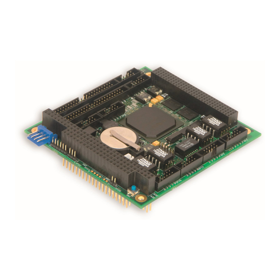
Summary of Contents for Fastwel CPC307
- Page 1 CPC307 PC/104-Plus Vortex86DX Based CPU Module User Manual Rev. 006 September 2022...
- Page 2 Product Title: CPC307 Document name: CPC307 User Manual Manual version: 006 Ref. doc. v.: 3.2 R (467444 038) Copyright © 2022 Fastwel Co. Ltd. All rights reserved. Revision Record Rev. Index Brief Description of Changes Board Index Date of Issue Initial preliminary version CPC307 v 2.0...
-
Page 3: Table Of Contents
Unpacking, Inspection and Handling ........................9 Three Year Warranty ............................. 10 Introduction ................................11 Purpose of the device ..........................11 CPC307 Versions, delivery checklist, ordering information ................ 12 1.2.1 Versions and ordering information…………………………………………………………………………..12 1.2.2 Delivery checklist………………………………………………………………………………………………13 Technical Specifications ............................. 16 General information on module functionality .................... -
Page 4: List Of Tables
CPC307 5.6 Chipset…………………………………………………………………………………………………………………103 5.7 Exit……………………………………………………………………………………………………………………...112 Guidelines on operation and use ........................114 Existing limitations and special features of the CPC307 module (ERRATA) ..........115 ANNEX A: LIST OF CHANGES IN THE MODULE VERSION 4.х.………….………………………………………116 ANNEX B: DISCLAIMER……………………..………………………………………………………………………..…117 List of Tables Table 1.1:... -
Page 5: List Of Figures
Location of connectors and main components on the TOP and BOTTOM for the CPC307-02, CPC307-05 versions (valid for CPC307 v.3.x)…………………………………...……..…………………..………………….…25 Figure 4.3: b) Location of connectors and main components on the TOP and BOTTOM sides of the CPC307- 02, CPC307-05 versions (relevant to CPC307 v.4.x)………………………………………………………………………..….26 Figure 4.4: a) Location of connectors and main components on the TOP and BOTTOM for the CPC307-03 version (valid for CPC307 v.3.x)…………………………………………………………………………………... - Page 6 This document contains information, which is property of Fastwel Co. Ltd. It is not allowed to reproduce it or transmit by any means, to translate the document or to convert it to any electronic form in full or in parts without antecedent written approval of Fastwel Co. Ltd. or one of its officially authorized agents.
-
Page 7: Notation Conventions
Introduction CPC307 Notation Conventions Warning, ESD Sensitive Device! This symbol draws your attention to the information related to electro static sensitivity of your product and its components. To keep product safety and operability it is necessary to handle it with care and follow the ESD safety directions. -
Page 8: General Safety Precautions
However, prolonged operation near the maximum temperature is not recommended by Fastwel or by electronic chip manufacturers due to thermal stress related failure mechanisms. These mechanisms are common to all silicon devices, they can reduce the MTBF of the product by increasing the failure probability. -
Page 9: Unpacking, Inspection And Handling
If damage is observed (usually in the form of bent component leads or loose socketed components), contact Fastwel's official distributor from which you have purchased the product for additional instructions. Depending on the severity of the damage, the product may even need to be returned to the factory for repair. -
Page 10: Three Year Warranty
In performing all necessary installation and application operations, please follow only the instructions supplied by the present manual. In order to keep Fastwel’s warranty, you must not change or modify this product in any way, other than specifically approved by Fastwel or described in this manual. -
Page 11: Introduction
This User Manual (hereinafter referred to as the User Manual or UM) presents general information on CPC307 CPU module (hereinafter referred to as the module), the details of its proper and safe installation, configuration and operation. The issues of PC/104 modules and external devices connection are also considered. -
Page 12: Cpc307 Versions, Delivery Checklist, Ordering Information
2хCAN, LAN 10/100, LPT, 4xUSB2.0, 8xGPIO, 2xI2C, PC/104-plus (ISA, PCI) format, COATED, from -50 up to +90 ºС Options available for CPC307: – Protective coating option (for CPC307-02, -03, -04 versions); \COATED – Preinstalled Linux 2.6 (for CPC307-02, -03, -05); \LNX Pre-installation on special order (for modules CPC307-02,-03,-05): \WCE5 –... -
Page 13: Delivery Checklist
РС104 box 155х140х45 mm IMES.467941.010 Packaging 1 pcs Table 1.3 shows a list of optional accessories for the CPC307 module, which are not included in the delivery checklist and can be purchased additionally. Table 1.3. Additional accessories for СРС307 Description... - Page 14 Introduction CPC307 Description Designation Ordering name ACS00031-03, ACS00031-03, Includes JST PHR-2 connector and SPH-002T-P0.5S pin ACS0054 ACS0054 set or 0.5 m crimped wire connector. Recommended mating part for the XP19 connector (opto- isolated reset/interrupt) ACS00038, ACS00038, Power socket with single pins (ACS00038) or crimped wire...
-
Page 15: Table 1.4: Differences Among The Supplied Configurations
Introduction CPC307 Table 1.4. Differences among the supplied configurations Ordering GPIO Format Coating number ATA Flash Disk (soldered, 1 GB РС104-plus (ISA, СРС307-02 for versions CAN 1-2 COM 1-6 GPIO PCI) before 4.x; 2 GB – for versions 4.х) ATA Flash Disk (soldered, 1 GB РС104-plus (ISA,... -
Page 16: Technical Specifications
333 MHz for module versions 4.х. Connection of HDD and optical disc drive for DVD/CD: 2 x connectors for microSD cards (only for CPC307-04, ATA Flash Disk is not installed); For other module versions connection of one additional IDE device is available;... -
Page 17: Power Requirements
XP22 power connector (4-pin AMP 4-171826-4 connector) can be used. For versions 3.x and below, the starting current of the module is 2.1 A for the CPC307-02 version. The power supply source must be capable of providing the starting current. A power supply source with a current limiting mode of at least 1.2 A can be used. -
Page 18: Operating Conditions
Technical Specifications CPC307 Table 2.1: Power Supply Requirements Starting current Connectors Maximum load Power Voltage Voltage limits current PC/104 и 2.1 (0.5 ms) – for +5 V From +4.75 to PC/104-plus +5.25V module versions lower than 4.х. 2.5 (0.5 ms) – for module versions 4.х. -
Page 19: Dimensions And Weight
Technical Specifications CPC307 Dimensions and Weight The module weight should not exceed the values specified in Table 2.3. 2.3. Module weight Version Net weight in Gross weight in kg, max kg, max CPC307-02 0.125 0.265 CPC307-03 0.120 0.260 CPC307-04 0.125 0.265... -
Page 20: Figure 2.1: A) Overall Dimensions Of Cpc307 Components And Their Locations (This Figure Is Valid For Ver.3X)
Technical Specifications CPC307 Figure 2.1 a) Overall dimensions of the CPC307 components and their locations (this figure is valid for versions 3.x) © 2 0 2 2 F a s t w e l v . 0 0 6 C P C 3 0 7... -
Page 21: Mtbf
Technical Specifications CPC307 Figure 2.2 b) Overall dimensions of the CPC307 components and their locations (this figure is valid for versions 4.х) 2.6 MTBF The MTBF values is 200, 000 hours. This MTBF value is calculated according to: Telcordia Issue 1 model, Method I Case 3, for... -
Page 22: Intended Use Of The Module
POST="Always", Terminal Display Mode="Recorder Mode" in the BIOS Setup menu. The more detailed description of the console settings are given in Section 5.2.3 Remote Access Configuration (Console I/O settings). – The CPC307-02,-03,-05 modules come with the FreeDOS operating system preinstalled on an ATA flash drive. © 2 0 2 2 F a s t w e l v . -
Page 23: Device And Operation
Device and operation Structure and Layout of main elements The module's block diagram is shown in Fig. 4. 1. Figure 4.1: CPC307 Block Diagram © 2 0 2 2 F a s t w e l v . 0 0 6... - Page 24 PS/2 keyboard/mouse port; Optoisolated external reset//interrupt signal, isolation voltage min.500V; 4 x USB 2.0 channels; Fast Ethernet port, 10/100 Mbit/s, isolation voltage min. 500V (except for CPC307-01); Serial ports: СОМ1: RS-232/422/485, up to 115.2 Kbaud, complete; ...
-
Page 25: Figure 4.2: A) Location Of Connectors And Main Components On The Top And Bottom For The Cpc307-02, Cpc307-05 Versions (Valid For Cpc307 V.3.X)
Device and operation CPC307 Figure 4. 2 a) Location of connectors and main components on the TOP and BOTTOM for the CPC307-02, CPC307-05 versions (valid for CPC307 v.3.x) © 2 0 2 2 F a s t w e l v . -
Page 26: Figure 4.3 B) Location Of Connectors And Main Components On The Top And Bottom Sides Of The Cpc307-02, Cpc307-05 Versions (Relevant To Cpc307 V.4.X)
Device and operation CPC307 Figure 4.3 b) Location of connectors and main components on the TOP and BOTTOM sides of the CPC307-02, CPC307-05 versions (relevant to CPC307 v.4.x) © 2 0 2 2 F a s t w e l v . -
Page 27: Figure 4.4 A) Location Of Connectors And Main Components On The Top And Bottom For The Cpc307-03
Device and operation CPC307 Figure 4.4 a) Location of connectors and main components on the TOP and BOTTOM for the CPC307-03 version (valid for CPC307 v.3.x) © 2 0 2 2 F a s t w e l v . 0 0 6... -
Page 28: Figure 4.5 B) Location Of Connectors And Main Components On The Top And Bottom Sides For The Cpc307-03 Version (Valid For Cpc307 V.4.X)
Device and operation CPC307 Figure 4.5 b) Location of connectors and main components on the TOP and BOTTOM sides for the CPC307-03 version (valid for CPC307 v.4.x) © 2 0 2 2 F a s t w e l v . 0 0 6... -
Page 29: Figure 4.6 A) Location Of Connectors And Main Components On The Top And Bottom For The Cpc307-04
Device and operation CPC307 Figure 4.6 a) Location of connectors and main components on the TOP and BOTTOM for the CPC307-04 version (valid for CPC307 v.3.x) © 2 0 2 2 F a s t w e l v . 0 0 6... -
Page 30: Figure 4.7 B) Location Of Connectors And Main Components On The Top And Bottom Sides For The Cpc307-04 Version (Relevant For Cpc307 V.4.X)
Device and operation CPC307 Figure 4.7 b) Location of connectors and main components on the TOP and BOTTOM sides for the CPC307-04 version (relevant for CPC307 v.4.x) © 2 0 2 2 F a s t w e l v . 0 0 6... -
Page 31: Address Space Allocation
Device and operation CPC307 4.2 Address Space Allocation 4.2.1 Address space allocation Table 4.1. Address space allocation of the first megabyte of memory Range of addresses Size Description 00000h – 9FFFFh 640 KB A0000h – BFFFFh 128 KB PCI/ISA VGA Graphics C0000h –... - Page 32 Device and operation CPC307 00B2h – 00BFh ISA bus Access to external bus 00C0h – 00DFh – 8237 DMA Controller #2 00E0h – 01EFh ISA bus Access to external bus 01F0h – 01F8h – Primary IDE Controller 01F9h – 0277h...
-
Page 33: Integrated Address Decoder
Device and operation CPC307 4.2.3 Integrated address decoder The module has two CAN controllers, the SJA1000T and a controller for two RS-232 serial ports, the XR16C2850IM. These controllers must be assigned with base addresses and address space ranges prior to their use. - Page 34 Device and operation CPC307 Base address, [31-0] for the memory address range, 31-1 [15-1] for I/O address range Address decoding authorization Chip Select 1 Base Address Mask 31-28 Reserved Reserved Enable decoding for read operations on the ISA bus (IOR#, MEMR#)
-
Page 35: Table 4.4: Preset Address Value For Can1 And Can2 Interfaces
Device and operation CPC307 - write the value 0DFFFFFC of the register of the base address mask to the port 0CFC. For CAN controllers on the module interrupts IRQ10 (CAN1) and IRQ11 (CAN2) are hardware set. The preset address values are specified in Table 4.4. -
Page 36: Distribution Of Interrupt Lines
By default, interrupt requests are generated by devices included in the module. The interrupt sources are shown in Table 4.6. Interrupt requests configuration is set in the BIOS Setup menu. Table 4.6. Distribution of interrupt lines in the CPC307 module Nodes that use interrupt... -
Page 37: Distribution Of Direct Memory Access Channels
Device and operation CPC307 4.2.5 Distribution of direct memory access channels Table 4.7. Distribution of direct memory access channels LPT - port PC/104 Connector (ISA) ● DREQ0 ○ ● DREQ1 ○ ● DREQ2 ○ ● DREQ3 ● DREQ5 ● DREQ6 ●... -
Page 38: Ddr2 Memory
Connection is carried out to the XP13 connector where the Primary IDE interface is routed. UDMA2 mode is supported. The CPC307-04 version is capable of connecting two microSD memory cards; see paragraph 4.3.4 MicroSD for a detailed description. If the soldered ATA Flash Disk controller is enabled, one additional external IDE-device can be connected to the module (Table 4.8). -
Page 39: Table 4.8: Possible Configurations For Connecting Ide Devices To The Module
Connection of two No connection devices For the CPC307-04 module make sure that no microSD cards are connected to the module and the "Parallel IDE" mode is selected in the BIOS Setup menu for the Primary IDE port (paragraph 5.2.2 IDE Configuration). -
Page 40: Table 4.10.Recommended Configurations For Ide Devices
Device and operation CPC307 DD11 IOCS16# DD12 PDIAG# DD13 DD14 CS0# CS1# DD15 DASP# – +5 В +5 В – Figure 4.9 Numbering of the XP13 connector pins The 2½” HDD connects directly to the XP13 using the ACS00010 cable (FC44). Other types of HDD (3½”... -
Page 41: Microsd
Device and operation CPC307 4.3.4 MicroSD Two microSD cards can be connected to the CPC307-04 version. Connection is made to the XS3 and XS4, which are connected to the SD interface. These connectors are for microSD and microSDHC memory cards only. -
Page 42: Ps/2-Keyboard And Mouse
Device and operation CPC307 4.3.6 PS/2-keyboard and mouse A keyboard and/or mouse with PS/2 interfaces can be connected to the module. This interface is routed to the XP23 6-pin connector. The interface is routed to the XP23 connector (IDC2-6, single-row, 2 mm male connector). -
Page 43: Usb Interface
Device and operation CPC307 - NMI interrupt generation (with the jumper installed on pins 5-6 of the XP25 connector). With such a configuration, the PFO# signal is switched to the IOCHK# line of the ISA bus. See also paragraph 4.3.20 Configuration jumpers, paragraph 4.3.19 GPIO ports. -
Page 44: Ethernet-Port
Device and operation CPC307 Booting from USB ports is supported, emulation (operation) mode and boot sequence are set in the BIOS Setup menu. Depending on the type and manufacturer of USB devices you may need to change the emulation mode and type or the system may be completely incompatible. Each specific USB device requires a separate compatibility check to ensure stable operation. -
Page 45: Serial Ports
Device and operation CPC307 The recommended mating part is 2039-3101 (ribbon cable press-on socket) or Leotronics 2022- 2102 (socket) and 2023-2000 set of contacts. Attention! At ambient temperatures below 0 ºC, the real exchange rate of the Ethernet port may decrease. -
Page 46: Figure 4.16: Pin Assignment Of The Xp18 Connector (For Module Versions 3.X And Lower)
Device and operation CPC307 For COM2, the RS-232 mode is set by shifting GPIO2 port line 2 to “1” and setting the direction of the line to “output”. RS-422/485 operation mode In RS-422/485 mode the ports work with hardware control of the transmitter and with the receiver permanently on. -
Page 47: Figure 4.17: A) The Rs-422/485 Transmitter With Bias Elements And Termination Resistors (For Ver.3.X & Lower)
Device and operation CPC307 resistors are used to ensure proper voltage levels in the inactive state of the network. A 2.2 kΩ protective bias resistor (Rcm+) is installed to set the initial high level on the TX+ line. To set an initial low level on the TX- line, a 2.2 kOhm protective bias resistor (Rcm-) is installed (Figure 4. -
Page 48: Figure 4.17: B) Rs-422/485 Transmitter With Bias Elements And With Terminating Resistors (For 4X Versions)
The maximum number of modules that can be connected to the RS-485 network together with the CPC307 module is 128, provided that the input impedance of the RS-485 drivers is minimum 96 . The maximum number of CPC307 modules combined within a single RS-485 network is no kΩ... -
Page 49: Table 4.15 Pin Assignment Of The Xp10 Connector For Com1 Port
Device and operation CPC307 Attention! A +5 V power supply circuit connects homonymous pins of XS1 (PCI-104), XS2 (PC- 104), and XP22 (additional power connector) connectors and is intended for supplying the module with power. The +5 V power supply outputs are protected by a 0.5 A fuse. -
Page 50: Figure 4.19: Connecting Several Devices Via Rs-422 Interface
Device and operation CPC307 Figure 4.20 shows connection of modules via RS-485 interface. Figure 4.19. Connecting several devices via RS-422 Interface Figure 4.20. Connecting several devices via RS-485 interface © 2 0 2 2 F a s t w e l v . -
Page 51: Table 4.17: Pin Assignment Of The Xp6 Connector For Com3 Port
Device and operation CPC307 4.3.10.2 COM3 and COM4 COM3 and COM4 ports are working in 9-wire RS-232 interface mode and have standard base addresses for PC/CAT. Base addresses and interrupt lines for the serial ports are selected in the BIOS Setup menu. -
Page 52: Table 4.19: Resources Assigned For Com5 And Com6 Controllers
The transmitters are controlled in RS-422/485 mode by hardware. The maximum number of modules that can be connected to the RS-485 network together with the module CPC307, is 128, provided that the input impedance of the RS-485 drivers is minimum 96 kΩ. -
Page 53: Figure 4.22: A) Pin Assignment Of The Xp15 And Xp20 Connectors (For Module Versions Older Than 4.Х)
Device and operation CPC307 XP15 - connection of terminating resistors for COM5 port, XP20 – connection of terminating resistors for COM6 port. Enabling Rtr for RX-/RX+ lines (COM6) Enabling Rtt for ТХ-/ТХ+ lines (COM6) Enabling Rtr for RX-/RX+ lines (COM5) Enabling Rtt for TX-/TX+ lines (COM5) Figure 4.22. -
Page 54: Figure 4.23 A) Transmitter With Protective Bias Elements And Terminating Resistors (For Ver. Lower Than 4.X)
Device and operation CPC307 resistor (Rcm+) is installed to set the initial high level on the TX+ line. A 2.2 kOhm (Rcm-) protective bias resistor is installed on the TX- line to set the initial low level (Figure 4.23 a) (for module versions older than 4.x)). -
Page 55: Table 4.20: Pin Assignment Of The Xp17 Connector For Com5 And Com6 Ports
The recommended mating part is Leotronics 2039-3101 (ribbon cable press-on socket) or Leotronics 2022-2102 (socket) and 2023-2000 set of contacts. The maximum number of CPC307 modules combined into a single RS-485 network is 16. Table 4.20. Pin assignment of the XP17 connector for COM5 and COM6 ports... -
Page 56: Printer Parallel Port (Lpt)
Device and operation CPC307 Figure 4.24. Numbering pins of the XP17 connector 4.3.11 Printer Parallel Port (LPT) The LPT1 parallel port operates in SPP, EPP, ECP mode and has the standard PC/AT standard PC/AT base addresses. Base address and interrupt line selection for the LPT1 port is carried out in the BIOS Setup. -
Page 57: Pc/104-Plus Connector
Device and operation CPC307 BUSY +5 В SLCT Figure 4.25. Numbering pins of the XP12 connector 4.3.12 PC/104-plus connector 4 x expansion cards with the PC/104-plus interface (PCI bus, 32 bits, 33 MHz, +3.3 V) can be connected to the module. Up to 3 x PCI-master devices are supported on the PC/104-plus bus. - Page 58 Device and operation CPC307 – – – TRDY# Input / Output – – FRAME# Input / Output – Power AD16 Input / supply Output – – – AD18 Input / Output AD21 Input / AD20 Input / Output Output –...
- Page 59 Device and operation CPC307 – – – AD15 Input / Output – – – Input / Output – – – – – – – – LOCK# PU (10K) Power supply – Power DEVSEL# Input / supply Output – – –...
-
Page 60: Pc/104 Connector
Device and operation CPC307 Figure 4.26. PCI-104 XS1 connector: a) module top view; b) module bottom view with organizer mounted on the connector Restrictions regarding installation of particular PC/104+ expansion boards on the module are described in Section 7. 4.3.13 PC/104 connector It is possible to connect additional expansion boards with the PC/104 interface (ISA bus, 8/16 bits, 8.3/16.6 MHz, DMA support) to the module. - Page 61 Device and operation CPC307 – SA15 Output DRQ3 Input SA14 Output DACK1# Output – SA13 Output DRQ1 Input SA12 Output REFRESH# Output SA11 Output Output – SA10 Output IRQ7 Input – Output IRQ6 Input – Output IRQ5 Input – Output...
-
Page 62: Can-Interfaces
Section 7. 4.3.14 CAN-interfaces The CPC307 module is equipped with two SJA1000T controller chips, compatible with the CAN 2.0b interface specification, and supports two independent CAN interface ports. There is a possibility of a software reset of the CAN controllers of each interface. The base address (BA) for the serial ports is selected by programming the registers of the Vortex86DX SoC. -
Page 63: Table 4.25: Pin Assignment Of The Xp5 Connector For Can1 And Can2 Ports
Device and operation CPC307 To connect the Rt terminating resistor to the CANL/CANH line, you must set a jumper to pins 3-4 (3-4 and 5-6 for 4.x module versions) of the XP8 connector for the CAN2 port. To enable the high-speed mode of the line driver, it is required to set a jumper to pins 1-2 of the XP8 connector for the CAN2 port. -
Page 64: Wdt Watchdog Timers
Device and operation CPC307 CANL (CAN2) GND_CAN2 Figure 4.29. Numbering pins of the XP5 connector Figure 4.30. Connection of the fail-safe biasing on CAN line 4.3.15 WDT watchdog timers The module uses 3 x WDT (Watchdog Timer) timers. The first two timers with programmable 30.5µs to 512s interval (WDT0, WDT1) are integrated into the Vortex86DX SoC. -
Page 65: Table 4.26: Description Of The Wdt0 Watchdog Timer Control Registers
Device and operation CPC307 Table 4.26 provides a detailed description of the WDT0 watchdog timer control registers. The registers of the timer WDT1 are accessed through the ports 67h - 6Dh. Table 4.27 provides a detailed description of the WDT1 watchdog timer control registers. -
Page 66: Table 4.27 Description Of The Wdt1 Watchdog Timer Control Registers
Device and operation CPC307 WDT0 timer status flag – timer was not triggered R/WC – timer was triggered (writing “1” to this bit resets the Address register flag) Writing “1” will make the WDT0 timer to restart. (22h) = 3Ch Writing “0”... -
Page 67: Rtc, Cmos, Fram, Hardware Reset And Bios Backup
Device and operation CPC307 µs Bits [23:16] of WDT1 timer, resolution – 30.5 WDT1 state register (value after 00h reset) WDT1 timer status flag – timer was not triggered R/WC – timer was triggered (writing “1” to this bit resets the... - Page 68 BIOS Setup values to the default. Turn the module on. Remote CMOS Reset for Windows 2000/XP. Version 1.0 Copyright (C) 2000, 2007 Fastwel Inc. Sending "reset" sequence through COM1. Press a key to abort ©...
- Page 69 Device and operation CPC307 - switch on the module’s power. - enter the module's BIOS SETUP and set the required BIOS settings. 4.3.16.3 Operation with FRAM Note The least-significant 1 KB of the FRAM memory is reserved! Writing to this area may cause non-stable operation of the module.
- Page 70 Device and operation CPC307 SI:CX:DX = MAC-address. The function returns the value stored in the FRAM MAC address field. The actual value, used by the controller may be different if it has been overwritten directly into the registers of the controller by the application software.
- Page 71 BIOS image file loaded, etc.). The current versions of the BIOS image files for the CPC307 module are available on the network file servers of the manufacturer and the official distributor, and are also provided upon the relevant request to the manufacturer's technical support service.
- Page 72 1. Install the jumper XP21, and do not install jumper XP26. Otherwise the backup copy cannot be updated. 2. Turn on the CPC307 module and boot up in a routing mode from the main BIOS copy. The WDT2 watchdog timer must not be triggered during the boot (par. 4.3.15.2 WDT2 watchdog timer).
- Page 73 (jumper XP26 is removed, the module is periodically reset), in this case you must: 1. Set the XP21 jumper and remove the XP26 jumper. 2. Power on the CPC307 module and boot from the BIOS backup copy (WDT2 watchdog will be triggered if the main BIOS copy is damaged).
- Page 74 Device and operation CPC307 After the module reboot, the optimal (factory default) BIOS Setup settings can be loaded. If necessary, enter the BIOS Setup, change the necessary parameters, save and exit (paragraph 5.7 Exit). 3. Run the main BIOS update program from the VXDXBIOS folder. You will need to specify the file name of the BIOS image for updating as the parameter: C:\VXDXBIOS\vxdxbios.exe c307v311.bin...
- Page 75 1. Copy the SPIFLASH folder from the relevant section of the FTP server to the module's boot disk. Place the updated BIOS image (for example, c307v310.bin file) in the copied folder. 2. Switch on the CPC307 module and boot into normal mode with the main BIOS copy under FreeDOS.
-
Page 76: Connecting Power Supply To The Module
4W, it is not allowed to power the entire stack through the XP22 connector of the CPC307 module. In this case, you should use the PC/104 sources that allow the stack to be powered via the PC/104 connector. -
Page 77: Module Power Supply Voltage Supervisor
Device and operation CPC307 4.3.18 Module power supply voltage supervisor When the +5V voltage is supplied, the ADM706T supervisor generates a module reset signal of 0.200 seconds duration (the “Powergood” signal will be set by inactive level “0”), provided that the supply voltage exceeds +3.08V. -
Page 78: Table 4.29: Description Of Gpio Ports
Boot control from external BIOS. 0 - unlock main BIOS chip, 1 - block main BIOS chip. (Hardware- GPIO1[5] Output controlled, changing port value is prohibited) Defining module type: 0 – CPC307-02/03, GPIO1[6] Input 1 – CPC307-04 Enabling the ATA Flash disk controller. Controlled by BIOS program. -
Page 79: Table 4.31: Pin Assignment Of The Xp14 Connector For Gpio0 Port
Device and operation CPC307 I/O line direction I/O port line Description Control of HL1 LED. 0 – disabled, GPIO2[4] Output 1 – enabled Control of HL2 LED. 0 – disabled, GPIO2[5] Output 1 – enabled State of the switch 1 of the SA1 switch unit. -
Page 80: Configuration Jumpers
Device and operation CPC307 4.3.20 Configuration jumpers Table 4.32. Description of setting the jumpers to the XP4 connector Jumper state Function When the jumper is set, the high-speed mode of the CAN1 interface driver is activated (for speeds higher than 250 Kb/s). -
Page 81: Table 4.36: Description Of Setting The Jumpers To The Xp18 Connector For Module Versions Lower Than 4.Х
Device and operation CPC307 Table 4.36. Description of setting the jumpers to the XP18 connector for module versions older than 4.х Jumper state Function When the jumper is set to TX+/TX- line of COM1 interface (in RS-422/485 1 - 2 mode), a 120 Ohm terminating resistor is connected. -
Page 82: Table 4.39 Description Of Setting The Jumpers To The Xp20 Connector For Module Versions 4.Х
Device and operation CPC307 Table 4.39 Description of setting the jumpers to the XP20 connector for module versions 4.х Jumper state Function Signal +TX is pulled up through the 680 Ohm resistor to the +5V power supply 1 - 2 voltage to generate a 200 mV offset on the Y/Z lines. -
Page 83: Table 4.42: Description Of Setting The Jumpers To The Xp21 Connector (For Module Versions Lower Than 4.Х)
Device and operation CPC307 Table 4.42. Description of setting the jumpers to the XP21 connector (for module versions lower than 4.х) Jumper state Function If the jumper is set, triggering the external watchdog timer of the module will make it restart from the BIOS backup copy. -
Page 84: Leds
Device and operation CPC307 4.3.21 LEDs There are 3 x LEDs on the module (HL1 to HL2). Assignment of the module LEDs is shown in Table 4.45. Table 4.45. Assignment of module LEDs Color Function Yellow Indication of +5 V supply voltage Green User LED. -
Page 85: Specific Features Of Console Redirect Module Operation
Device and operation CPC307 4.3.22 Specific features of console redirect module operation BIOS has a console redirect module, designed to work with the board in the terminal mode. To continue the module's operation after OS startup you must enable BIOS Setup option “Redirection After BIOS →... -
Page 86: Basic Input/Output System (Bios)
Depending on the BIOS version, the number and values of menu items may differ from the description of the v.3.11 BIOS version for the CPC307 v.3.1 modules below. To get a hint about the function keys used for easy navigation through the menu items, press the F1 key after entering the BIOS Setup. -
Page 87: Main
Device and operation CPC307 5.1 Main This tab contains a description of the BIOS version, the installed CPU and RAM. There are also two items responsible for setting the current time and date. The screen view of the “Main” menu is shown in Figure 5.2, the description of the items is given in Table 5.1. -
Page 88: Advanced
“power up” ATA Flash Controller NAND controller is hardware switched “power down” state No NAND controller “unknown or SD” (version CPC307-04 or version 3.x) Embedded NAND The soldered ATA Flash Disk controller is enabled Flash 1), 2) [Enabled] Operations is enabled... -
Page 89: Table 5.3: Description Of The "Cpu Configuration" Menu
Notes: 1) Version 3.x modules do not have the "Embedded NAND Flash" feature; 2) The CPC307-04 version has no "Embedded NAND Flash" function. 5.2.1 CPU Configuration The “CPU Configuration” menu screen is shown in Figure 5.4, description of the items is given in Table 5.3. -
Page 90: Table 5.4: Description Of The "Ide Configuration" Menu
Controls operation of the integrated IDE bus controller. (item is present only for [SD Card] Operation of the IDE controller in SD card support mode the module CPC307-04) [Parallel IDE] Operation of the IDE controller in IDE device support mode Primary IDE Master This menu item contains information about the connected IDE device operating in Master mode (Figure 5.5, Table 5.3). -
Page 91: Table 5.5 Description Of The "Primary Ide Master" Menu
Device and operation CPC307 Hard Disk Write Protect Access denial to writing to IDE devices [Enabled] Enable denial [Disabled] Disable denial IDE Detect Time Out Time limit for ATA/ATAPI device detection, in sec. The following values are (Sec) available: [0], [5], [10], [15], [20], [25], [30] ,[35]... - Page 92 Device and operation CPC307 [ARMD] Detect the connected device as an ATAPI Removable Media Device (ZIP, LS-120) LBA/Large Mode Addressing type of the device connected to this IDE channel [Auto] Automatic detection of LBA Mode support [Disabled] Disabled detection of LBA Mode, Large Mode is used...
-
Page 93: Table 5.6: Description Of The "Remote Access Configuration" Menu
Device and operation CPC307 5.2.3 Remote Access Configuration The Remote Access Configuration menu screen is shown in Figure 5. 7, the description of the items is given in Table 5. 6. Figure 5.7. Screen of the “Remote Access Configuration” menu Table 5.6. - Page 94 Device and operation CPC307 [None] None [Hardware] CTS/RTS hardware control [Software] XON/XOFF software control Redirection After BIOS Redirection After BIOS POST POST [Disabled] Disable remote access after the BIOS POST procedure [Boot Loader] Remote access is active during BIOS POST and OS boot [Always] Remote access is always active.
-
Page 95: Table 5.7 Description Of The "Usb Configuration" Menu
Device and operation CPC307 5.2.4 USB Configuration The “USB Configuration” menu screen is shown in Figure 5.8, the description of the items is given in Table 5.7. Figure 5.8. Screen of the “USB Configuration” menu Table 5.7 Description of the “USB Configuration” menu... -
Page 96: Table 5.8: Description Of The "Usb Mass Storage Device Configuration" Menu
Device and operation CPC307 5.2.5 USB Mass Storage Device Configuration The “USB Mass Storage Configuration” menu is shown in Figure 5.9, the description of the items is given in Table 5.8. Figure 5.9. Screen of the “USB Mass Storage Device Configuration” menu Table 5.8. -
Page 97: Pcipnp
Device and operation CPC307 5.3 PCIPNP This tab contains items responsible for PCI and ISA bus operation as well as interrupt switching control. The screen view of the PCIPnP menu is shown in Figure 5.10, the menu description is given in Table 5.9. - Page 98 Device and operation CPC307 [No] [Yes] PCI Latency Timer The maximum number of PCI bus cycles during which the device connected to the bus can keep it busy by transmitting data. [32], [64], [96], [128], [160], [192], [224], [248] Allocate IRQ to PCI VGA...
-
Page 99: Boot
Device and operation CPC307 5.4 Boot This tab contains items responsible for the module's boot modes, as well as for selecting the IDE device from which the operating system will be booted. The screen view of the “Boot” menu is shown in Figure 5.11, description of the menu items is given in Table 5.10. -
Page 100: Table 5.11: Description Of The "Boot Settings Configuration" Menu
Device and operation CPC307 5.4.1 Boot Settings Configuration The "Boot Settings Configuration" menu screen is shown in Figure 5.12, the description of the menu items is given in Table 5.11. Figure 5.12. Screen of the “Boot Settings Configuration” menu Table 5.11. Description of the “Boot Settings Configuration” menu... - Page 101 Device and operation CPC307 [Disabled] Support is disabled [Enabled] Support is enabled [Auto] Support is detected automatically. Recommended value Wait for ‘F1’ If Error Waiting for “F1” key to be pressed in case of error [Disabled] This option does not require to wait for user intervention in case of an error.
-
Page 102: Security
Device and operation CPC307 5.5 Security The “Security” menu screen is shown in Figure 5.13. The description of the menu items is given in Table 5.12. Figure 5.13. Screen of the “Security” menu Table 5.12. Description of the “Security” menu... -
Page 103: Chipset
Device and operation CPC307 5.6 Chipset The “Chipset” menu screen is shown in Figure 5.14. Description of the menu items is given in Table 5.13. Figure 5.14. Screen of the “Chipset” menu Table 5.13. Description of the “Chipset” menu Menu item... -
Page 104: Table 5.14: Description Of The "South Bridge Configuration" Menu
Device and operation CPC307 5.6.1 South Bridge Configuration The South Bridge Configuration menu screen is shown in Figure 5.15, description of the menu items is given in Table 5.14. Figure 5.15. Screen of the “South Bridge” menu Table 5.14. Description of the “South Bridge Configuration” menu... -
Page 105: Figure 5.16: Screen Of The "Isa Configuration" Menu
Device and operation CPC307 LAN IRQ Assigning interrupt to the Ethernet (LAN) controller [Auto] Automatic detection [IRQ 5] Assign interrupt #5 [IRQ 10] Assign interrupt #10 [IRQ 15] Assign interrupt #15 [IRQ 6] Assign interrupt #6 MAC Address MAC address of the integrated Ethernet (LAN) controller... -
Page 106: Table 5.15: Description Of The "Isa Configuration" Menu
Device and operation CPC307 Table 5.15. Description of the “ISA Configuration” menu Menu item Purpose ISA Clock Clock frequency ISA_SYSCLK (CLK, XS2 connector, output B20) [8.3MHz] Set the clock frequency for 8 MHz [16.6MHz] Set the clock frequency for 16 MHz... -
Page 107: Table 5.16: Description Of The "Serial/Parallel Port Configuration" Menu
Device and operation CPC307 Table 5.16. Description of the “Serial/Parallel Port Configuration” menu Menu item Purpose SB Serial Port 1 This option sets the address for the corresponding serial port (separately for each port) SB Serial Port 2 [Disabled] Port operation is disabled... -
Page 108: Table 5.17: Description Of The "Watchdog Configuration" Menu
Device and operation CPC307 [ECP AND Operating mode compatible with ECP and EPP 1.7 modes EPP 1.7] Parallel Port IRQ This option assigns an interrupt line for the LPT1 parallel port [IRQ5] IRQ5 interrupt line assignment [IRQ7] IRQ7 interrupt line assignment 5.6.1.3 WatchDog Configuration... -
Page 109: Table 5.18: Description Of The "Gpio And I2C Configuration" Menu
Device and operation CPC307 WatchDog 0 Timer Sets the time interval for the corresponding timer counting. The Watchdog timer counts backwards during operation. If the value is set to 64 seconds, it will count WatchDog 1 Timer down to 0 and then generate a RESET, NMI or IRQ signal. If the timer receives a... - Page 110 Device and operation CPC307 Pin Select [2xI2C Bus] Two I2C ports [GPIO [7..4]] Lines of the GPIO 0 I/O port Sets the port lines to “input” or “output” state. Each line can be individually set as “input” GPIO PORT0 78H [7..4] FUNC or "output...
-
Page 111: Table 5.19: Description Of The "Can And Com5,6 Configuration" Menu
Device and operation CPC307 5.6.1.5 CAN and COM5,6 Configuration The screen of the “CAN and COM5,6 Configuration” menu is shown in Figure 5.20, description of the menu items is shown in Table 5.19. Figure 5.20. Screen of the “CAN and COM5,6 Configuration” menu Table 5.19. -
Page 112: Exit
Device and operation CPC307 5.7 Exit The “Exit” menu screen is shown in Figure 5.21. Description of the menu items is given in Table 5.20. Figure 5.21. Screen of the “Exit” menu Table 5.20. Description of the “Exit” menu Menu item... - Page 113 Device and operation CPC307 5.8 Functional limitations of BIOS versions BIOS version 3.12 (Core Version 8.00.15, build date 31/01/2012) pre-installed in modules version 3.1, has the following functionality limitations: 1. Skipping the load of Autoexec.bat by the Ctrl+B command through the input/output console has been adjusted.
-
Page 114: Guidelines On Operation And Use
CPC307 module; • where there is a PCI connector organizer on the Expansion Module: installation would be possible only on the bottom side of the CPC307 module. © 2 0 2 2 F a s t w e l v . -
Page 115: Existing Limitations And Special Features Of The Cpc307 Module (Errata)
CPC307 7 Existing limitations and special features of the CPC307 module (ERRATA) In the CPC307, PP 687263.012 v3.x modules, disabling the internal storage (NAND Flash) during operation is impossible. © 2 0 2 2 F a s t w e l v . -
Page 116: Annex A List Of Changes In The Module Version 4.Х
Device and operation CPC307 Annex A List of changes in the module version 4.х 1. Switching of bias resistors for RS-422/485 ports has been changed. 2. Integrated drive capacity has been increased to 2 GB. 3. Additional XP27 jumper for reset of BIOS settings has been implemented BIOS. -
Page 117: Annex:b Disclaimer
1.2 Use of the Fastwel products as well as the objects of intellectual property containing in them, in the ways and for the purposes, not provided by the present user manual and datasheet isn't allowed without preliminary written approval of Fastwel.
Need help?
Do you have a question about the CPC307 and is the answer not in the manual?
Questions and answers