
Subscribe to Our Youtube Channel
Related Manuals for Fastwel KIC551


Summary of Contents for Fastwel KIC551
- Page 1 KIC551 Interface Module in 3U CompactPCI Serial format User Manual Rev. 003 September 2021 The product described in this manual is compliant with all related CE standards.
- Page 2 Product Title: KIC551 Document name: KIC551 User Manual Manual version: 003 Ref. docs: Copyright © 2021 Fastwel Co. Ltd. All rights reserved. Revision Record Rev. Index Brief Description Product Index Date Preliminary version KIC551/ KIC551RC August 2017 Initial version KIC551/ KIC551RC...
-
Page 3: Table Of Contents
Battery replacement ………………………………………………………………………………………………...47 Program configuration of KIC551/KIC551RC ................... 51 Modification of operating software ......................51 Upgrading configuration software via Gigabit Ethernet interface of the KIC551/KIC551RC module ..…..54 4.2. ANNEX A: List of FPGA internal function registers ……..…………………………………………………………..………78 ANNEX B: List of Telnet Interface Commands ………………………………………………………………………..………80 ANNEX C: Characteristics of the peripherals’... -
Page 4: List Of Tables
Paramters of KIC551/KIC551RC power consumtpion…………………………………………………..39 Table 3-2: Measurements results of starting current and average current consumption ........39 Table 3-3: Paramters of climatic and mechanical effects (KIC551) ..............40 Table 3-4: Paramters of climatic and mechanical effects (KIC551RC) ............. 41 Table 3-5: Dissipated power and limit temperatures of microchips.............. -
Page 5: List Of Figures
This document contains information, which is property of Fastwel Co. Ltd. It is not allowed to reproduce it or transmit by any means, to translate the document or to convert it to any electronic form in full or in parts without antecedent written approval of Fastwel Co. Ltd. or one of its officially authorized agents. - Page 6 KIC551 interface module with forced cooling and KIC551RC interface module with conduction cooling (hereinafter referred to as the device or KIC551/KIC551RC) and contains description, principle of operation, technical specs of KIC551/KIC551RC, as well as establishes rules of its operation. You should read this User Manual before using the product.
- Page 7 KIC551 Ownership rights This document contains information that is the property of Fastwel Group. It may not be copied or transmitted by any known means, nor may it be stored in information storage and retrieval systems without the prior written consent of Fastwel Group or one of its authorized agents. The information...
- Page 8 KIC551 Conventions Caution, High Voltage! This sign and text warn of the dangers associated with electrical discharges (> 60 V) when touching the device or any part of it. Failure to follow the precautions mentioned or prescribed in the regulations may endanger your life or health, and may result in damages to the equipment.
- Page 9 KIC551 Safety requirements This Fastwel Group product has been developed and tested to ensure compliance with electrical safety requirements. Its design provides long-term fail-safe operation. The product's life cycle may be significantly shortened due to mishandling during unpacking and installation. Therefore, for your own safety and for ensuring proper operation of the device, you should follow the recommendations given below.
-
Page 10: General Rules Of Usage
Fastwel Group other than those contained in this User Manual or received from the technical support service of Fastwel Group in the form of a set of instructions for their implementation will void the warranty. - Page 11 KIC551 Limitation of warranty obligations The above warranty does not apply to: - the products (including software) that have been repaired or modified by the employees who do not represent the Manufacturer. The exception is when the Consumer has made repairs or made changes to the product strictly in accordance with the instructions previously agreed and approved by the Manufacturer in writing;...
-
Page 12: Transportation, Unpacking And Storage
KIC551 Transportation, Unpacking and Storage Transportation The modules should be transported in the separate manufacturer’s packaging (container), consisting of an individual antistatic packaging and a cardboard box, in closed transport (road, rail, air in heated and sealed compartments) under storage conditions 5 according to the GOST standard 15150-69 or under storage conditions 3 for sea transportation. -
Page 13: Description And Operation Of Kic551/Kic551Rc
Ethernet interfaces and is designed to transfer packets between peripheral slots and an external device (see subparagraph 1.4). The KIC551 is designed so as to provide consumers with an integrated 3U CPCI Serial solution for the use in real-time systems, manufacture control, high-speed data acquisition and data processing. - Page 14 ▪ SFF-8431 Specifications for Enhanced Small Form Factor Pluggable Module SFP+. ■ Power supply: ▪ Supply voltage: + 12 V, + 5 V_standby. ■ Operating temperature range of KIC551: ▪ Industrial version: from - 40 to +85 °C; ▪ Commercial version: from 0 to +70 °C.
-
Page 15: Structural Features Of Kic551Rc
4HP; from -40 to +85 °C. IMES.421459.551-03 KIC551-02-I For ordering KIC551 with a conformal coating, you will need to add \ Coated option to the above. E.g. KIC551-01 \ Coated. Photo of KIC551 is shown in Fig. 1.1. © 2 0 2 1... -
Page 16: Ordering Information For Kic551Rc
KIC551 1.6 Ordering information for KIC551RC KIC551RC is manufactured in accordance with Table 1.2: Table 1.2 – Versions of KIC551RC Name Number Ordering name Note PCIe and Ethernet switch with PCIe optical IMES.467449.003 KIC551RC-01 interface, equipped with a conduction-type cooling unit, 5HP. -
Page 17: Location Of Components And Overall Dimensions Of Kic551
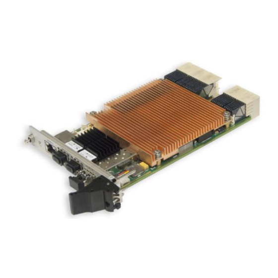
1.7.1 Overall view of KIC551 Fig. 1.1 show the external view of KIC551-01 with the installed finned heatsink (4HP). The front panel of KIC551-02 has no connectors of PCIe optical interface (the differences between the versions of the KIC551 module are shown in Table 1.1 – Versions of KIC551), specified on KIC551-01 as RX and TX (see Fig. - Page 18 Fig. 1.2 shows the top side of the KIC551-01 module (heatsink is not shown). Fig. 1.2 – Location of main components of KIC551, top view (as exemplified by KIC551-01) The appearance of the module versions may slightly differ from the one shown in figure.
- Page 19 KIC551 1.7.3 Front panel of KIC551 Fig. 1.3 and Fig. 1.4 show the front panels of KIC551-01 and KIC551-02, respectively. Fig. 1.3 – Front panel of KIC551-01 Fig. 1.4 – Front panel of KIC551-02 The appearance of the module versions may slightly differ from the one shown in figure.
- Page 20 KIC551 1.7.4 Overall dimensions of KIC551 Fig. 1.5 demonstrates KIC551-01 with indication of overall dimensions. Fig. 1.5 – Overall dimensions of KIC551 © 2 0 2 1 K I C 5 5 1 U s e r M a n u a l F a s t w e l V e r .
-
Page 21: Location Of Elements And Overall Dimensions Of Kic551Rc
1.8.2 Front panel of KIC551RC Fig. 1.7 shows the front panel of the KIC551RC-01 module specifying structural elements. Same as with the KIC551-02 convection cooling module (Fig. 1.4), the front panel of KIC551RC-02 has no PCIe optical interface connectors (RX and TX). - Page 22 KIC551 Fig. 1.7 – Main components of KIC551RC front panel (as shown by KIC551RC-01) The appearance of the module versions may slightly differ from the one shown in figure. A and B handles are designed for installation/removal of KIC551RC (see subparagraphs 3.7.4 Procedure for installation of KIC551RC and 3.7.5 KIC551RC removal procedure).
-
Page 23: Delivery Checklist Of Kic551/Kic551Rc
Fig. 1.8 shows KIC551RC-01 with indication of overall dimensions. Fig. 1.8 – Overall dimensions of KIC551RC 1.9 Delivery checklist of KIC551/KIC551RC The delivery checklist includes the following: ▪ KIC551 or KIC551RC module; ▪ package. ... -
Page 24: Packaging Information
KIC551 1.10 Packaging information KIC551/KIC551RC placed in an antistatic bag, is supplied in the box with overall dimensions of 350 x 260 x 70 mm. Table 1.3 – Packed weight of KIC551 and KIC551RC Name Packed module weight, no more than, g... -
Page 25: Description And Operation Of Subsystems Of Kic551/Kic551Rc
KIC551 2 Description and operation of subsystems of KIC551/KIC551RC 2.1 Block diagram The block diagram for KIC551/KIC551RC is shown in Fig. 2.1. Fig. 2.1 – Block diagram for KIC551/KIC551RC ... -
Page 26: Description And Operation Of Functional Nodes
The switch provides data exchange between the modules in peripheral slots and an external device connected to the front panel of the KIC551/KIC551RC module. SGMII is used as the communications interface with the PHY layer (by 88E1340S and 88E1111 controllers). -
Page 27: Description Of Kic551/Kic551Rc Module's Units
Due to the fact that the proper functioning of the system unit depends on the performance of the KIC551 / KIC551RC module, appropriate measures were taken at the time of designing the module to increase the durability of its main units with the possibility of duplication and emergency recovery. - Page 28 KIC551 Fig. 2.2 – Diagram of the main units of KIC551/KIC551RC © 2 0 2 1 K I C 5 5 1 U s e r M a n u a l F a s t w e l V e r . 0 0 3...
- Page 29 EEPROM, as well as real time clock. ■ FPGA The FPGA chip installed on the KIC551 / KIC551RC module is designed for performing the following functions: ▪ Controlling the process of supplying power to the units of the PCI Express interface module: units of the PEX8764 PCI Express switch, 10 Gbit Ethernet JL82599EN, optical modules.
- Page 30 NAND drive can be organized through the Gigabit Ethernet switch from any peripheral slot of the system or through the RJ45 connector on the front panel of the KIC551/KIC551RC module. A detailed description of works with the NAND drive is given in Section 4 Program configuration of KIC551/KIC551RC.
- Page 31 KIC551 Fig. 2.3 – Diargam for multiplexing configuration EEPROM of KIC551/KIC551RC The board of the KIC551 / KIC551RC module is also equipped with hardware multiplexers (SN74CBTLV3257), which arrange switching of interfaces (SPI or Microware) of the corresponding configuration EEPROMs between the FPGA and the configured devices themselves. These...
-
Page 32: Table 2-1: Status Of The Hl13 Led
HL13 LED is designed to determine the current active configuration EEPROM (Fig. 2.4, Table 2.1, subparagraph 4.2.5 Booting the Program Configuration Unit’s FPGA (main/reserved)). Fig. 2.4 – Location of H13 LED and power supply battery connector on KIC551/KIC551RC Table 2.1 – Status of the HL13 LED... -
Page 33: Table 2-2: Led Unit
Green/Red Temperature mode of the module UP (GP) Green/Red Status of the optical PCI Express interface (KIC551-01 and KIC551RC-01). The GP LEDs functions are reserved. ■ PE1 – PE8 LEDs The PE1 – PE8 LEDs (Fig. 2.5) are designed for designating parameters of the PCI Express connection in each peripheral slot. -
Page 34: Table 2-3: Status Of Pe1 - Pe8 Leds
KIC551 The information displayed by PE1 – PE8 LEDs is given in Table 2.3. Table 2.3 – Status of PE1 – PE8 LEDs LED color Display mode Status of the PCI Express connection Connection speed – 8 Gb Green Permanently Connection speed –... -
Page 35: Table 2-6: Status Of Sys Led
The UP LED (Fig. 1.7, Fig. 2.6 (a)) is designed for displaying parameters of the PCI Express connection of optical interface represented with KIC551-01/KIC551RC-01 versions. The data for display is generated by hardware: by the integrated features of the PCI Express switch. -
Page 36: Table 2-9: Status Of Up Led
2.3.3 Synchronization unit The synchronization unit is designed for generating clock pulses with specified characteristics both for the nodes of the KIC551 / KIC551RC module itself and for peripheral modules installed into the system backplane. In terms of design, the synchronization unit is made of three parts: driving quartz-crystal oscillator, uncrontrolled bffer for integrated nodes and controlled 8-channel buffer for peripheral modules. - Page 37 HX5200NL Dual Transformer Modules. To connect an external Gigabit Ethernet network on the front panel of KIC551 there is a Gigabit Ethernet port, connected to one of the switch channels via a separate PHY Marvell 88E1111 Gigabit Ethernet Transceiver.
-
Page 38: Table 2-10: Purpose Of The Rj45 Gigabit Ethernet Connectors' Pins
Galvanic isolation of the Gigabit Ethernet port routed to the front panel is 500 volts. 2.3.6 10G Ethernet network controller unit The 10 Gbit Ethernet network controller unit is designed for arranging connection of the system with the KIC551 / KIC551RC module to external devices via the 10 Gbit Ethernet interface. ® Intel... -
Page 39: Cooling System Of Kic551
At the time of operation, the system considers the optical transmission line as a traditional connection over the PCI Express interface. The optical connection status is shown by the UP LED located on the front panel of KIC551- 01/KIC551RC-01 (Fig. 2.6 (a)). Operational behavior of the UP LED is described in the Table 2.9 (Subparagraph 2.3.2). -
Page 40: Cooling System Of Kic551Rc
Requirements for the cooling system of the KIC551 modules are given in subparagraph 3.6.1. 2.4.1.1 Data-transfer-rate-Temperature releationship (KIC551) To confirm the stated characteristics, climatic tests of the KIC551 modules were carried out. Before the start of the tests, fans were installed into the chassis, which were turned on throughout the entire experiment. -
Page 41: Intended Use
3 Intended Use 3.1 Power consumption of KIC551/KIC551RC The supply voltage of the KIC551 / KIC551RC is +5 V_ standby, +12 V. The specified requirements must be taken into account that are essential to ensure stability and reliability. Table. 3.1 shows the values of the maximum permissible voltages on the power lines, exceeding which may damage the module. -
Page 42: Compliance With Safety Requirements Of Kic551/Kic551Rc
KIC551 3.2 Compliance with safety requirements of KIC551/KIC551RC KIC551/KIC551RC corresponds to the general safety requirements for IT equipment in accordance with the GOST R IEC 60950-2002 (for equipment powered from the mains with voltages up to 600V). 3.3 Electromagnetic compatibility of KIC551/KIC551RC KIC551/KIC551RC corresponds to the requirements for resistance of IT equipment against electromagnetic interference in accordance with the GOST CISPR 24-2013. -
Page 43: Kic551Rc Operating Conditions
3.6 Cooling system requirements Attention!!! Since Fastwel Group is not responsible for any damages to KIC551/KIC551RC and other equipment, caused by overheating, the system developers and end users are recommended to ensure that the module's environment complies with the specified temperature requirements (see subparagraphs 3.6.1 and 3.6.2). -
Page 44: Table 3-5: Dissipated Power And Limit Temperatures Of Microchips
The module should operate within the specified temperature ranges (subparagraph 1.2 Technical Feaures of KIC551/KIC551RC, Table 3.3) with the forced air cooling as part of the chassis. The total power dissipated by PCI Express and Gigabit Ethernet switches as well as by 10 Gbit Ethernet network controller is ~50 W. -
Page 45: Installation And Removal
3.7.1 Safety rules during installation and removal of the module The KIC551 / KIC551RC module is easy to install. At the same time, the below rules, warnings and procedures must be strictly followed in order to properly install the module, avoid any damages to it, its system components, and prevent personal injuries. - Page 46 ▪ Fix the module to the front panel of KIC551 using two retention screws (see Fig. 1.3, Fig. 1.4). ▪ Connect all necessary external interface cables to the module.
- Page 47 The subsequent operations should be performed with care to avoid damaging both KIC551 and other devices of the system. 2. Prior to start the removal of KIC551, make sure that system power supply is off. 3. Disconnect all interface cables from the module.
- Page 48 KIC551 Attention! The following operations should be performed with caution, in order not to damage either KIC551RC, or other devices of the system. 3. For installing KIC551RC the following actions should be performed: ▪ Prior to installation, make sure that the system power supply is off.
-
Page 49: Battery Replacement
3.9 Configuration of KIC551/KIC551RC Configuration of the KIC551/KIC551RC module includes hardware and software parts. 3.9.1 Hardware configuration of the KIC551/KIC551RC module The hardware part includes 8 microswitches (located in the bottom part of the module), divided into two groups, where each group contains 4 microswitches: SA1 and SA2 (see Fig. -
Page 50: Table 3-7: Box Of Sa1 Microswitches
▪ Blocking the use of the software component of the module configuration. ▪ Switching the software configuration of the KIC551module depending on the version: with conduction cooling of KIC551RC or finned heatsink of KIC551. ● Setting the box of SA1 microswitches Functions of the SA1 box are individual for each microswitch, included in the box. -
Page 51: Table 3-8: Box Of Sa2 Microswitches
It is recommended to use CPC51x Compact PCI Serial standard processor modules as the slave devices, but only those manufactured by Fastwel Group. Descirption of the SA2 microswitch box is given in the Table 3.8. - Page 52 3.9.2 Program configuration of the KIC551/KIC551RC module Program componenet makes it possible to perform a more flexible configuration of KIC551/KIC551RC nodes’ parameters. The program component settings are stored in the system Program Configuration Unit, written to the speciflized EEPROM. In addition to the settings specified for the hardware component, the software component settings...
-
Page 53: Program Configuration Of Kic551/Kic551Rc
PC via RJ45 cable with the 1 Gb Eth connector, located on the front panel of KIC551/KIC551RC (Fig. 2.7). After feeding the power to KIC551/KIC551RC you should start the Telnet-client program on the external PC, e.g. “PuTTY” utility or similar. - Page 54 The Telnet-session window will be closed automatically. Further you should start any Internet browser program. In the opened window of the program, in the address bar specify the KIC551 module’s address: 192.168.0.10: Enter the username in the User ID line. By default: admin The Password line should contain password.
- Page 55 After the programming, the KIC551/KIC551RC module should be turned off. 4.1.1 Formatting the integrated NAND drive The NAND drive mounted on the KIC551/KIC551RC module is designed for storing alternative system configurations, as well as for backup storing configuration software for all peripheral devices of the module.
- Page 56 The formatting mode with erasing all the packs will take some time. You should wait for the message that the procedure has been completed successfully. After formatting the NAND drive, the KIC551 module will be ready for loading the pack of configuration parameters.
-
Page 57: Upgrading Configuration Software Via Gigabit Ethernet Interface Of The Kic551/Kic551Rc Module
Choosing EEPROM bit 1, see Table 4.2. Bit0 Choosing EEPROM bit 0, see Table 4.2. The KIC551/KIC551RC module has a total of 6 individually addressable EEPROM chips (Table 4.2). Compliance of bit sequences of the register with the address 01 “EEPROM Control” with the selected EEPROM microchip is shown in the Table 4.2. -
Page 58: Table 4-2: Compliance Of Bit Sequences Of The Register With The Address 01 "Eeprom Control" With The
Each of the listed PCUs, is in operating condition and stored in the corresponding EEPROM chip, from where it is loaded when the KIC551 / KIC551RC module is powered on. If PCU needs to be changed, the updated PCU is placed into the NAND drive of the... - Page 59 Where the microcontroller functions properly, the settings of these microchips are performed by the microcontroller itself when power is supplied to the KIC551/KIC551RC module. If the microcontroller turns out to be inoperable and faulty for any reason, the PCU parameters contained in the configuration EEPROM are automatically used.
- Page 60 In order for the changes to take effect (for the newly written configuration to become active), you should perform the power supply on/off switching cycle of the KIC551/KIC551RC module. 4.2.4 Booting the Program Configuration Unit of the 10 Gbit Ethernet controller...
- Page 61 5. Confirmation that multiplexer has returned to the initial state. In order for the changes to take effect (for the newly written configuration to become active), you should perform the power supply on/off switching cycle of the peripherals of the KIC551/KIC551RC module.
- Page 62 The figure shows that V=10. That means that the Program Configuration Unit has the version 1.0. Attention! Working Program Configuration Unit’s FPGA of the KIC551/KIC551RC module is provided by the manufacturer or its authorized representatives. Loading the Program Configuration Unit created by other persons may result in blocking the operation of the KIC551 module.
- Page 63 In order for the changes to take effect (for the newly written configuration to become active), you should perform the power supply on/off switching cycle of the KIC551/KIC551RC module or use the program initialization of FPGA by means of the microcontroller (where the peripheral devices connected to the KIC551/KIC551RC module will also be initialized).
- Page 64 In order for the changes to take effect (for the newly written configuration to become active), you should perform the power supply on/off switching cycle of the KIC551/KIC551RC module or use the FPGA program initialization by means of the microcontroller (where the peripheral devices connected to the KIC551/KIC551RC module will also be initialized).
- Page 65 In order for the changes to take effect (for the newly written configuration to become active), you should restart the system or, depending on the type of changes made into the new Program Configuration Unit, perform the power supply on/off switching cycle of the KIC551/KIC551RC module.
- Page 66 Alongside with the management functions, the microcontroller supports the following control functions: ▪ The values of the main power supply voltages of the KIC551/KIC551RC module (LM87 resource). ▪ The temperature values of the of the KIC551/KIC551RC module’s PCB (LM87 resource).
-
Page 67: Table 4-3: Register 03, Bit 0
KIC551 ▪additionally: output of standby voltage “+5 V_standby” (5VSB) with load current no less than 3 A. Control input PS_ON# of the power supply source should be connected to the “Utility Connector”, located on the crate’s backplane. The system power is managed in accordance with the Table 4.3 by setting or resetting bit 0 of the “Power Control”... -
Page 68: Table 4-4: Register 05, Bit 0
The function of the optical receiver and transmitter modules initialization makes it possible to disable the specified elements of the KIC551-02/KIC551RC-02 module by a forced installation of the "Reset" line of the optical modules to the active state. -
Page 69: Table 4-6: Register 05, Bit 2
KIC551 To disable optical modules: - Reading the current state of the “System Control” register. Further, in the CMD>rfr 05 read value, bit 1 should be set (for example, for the read value V = 08h). To disable the optical modules, bit 1 of register 05 is set by the following command: CMD>wfr 050A... -
Page 70: Table 4-7: Register 05, Bit 3
KIC551 The function is accessed via bit 3 of the “System Control” register with address 05 (Table 4.7). Table 4.7 – Register 05, bit 3 State Function 10 Gbit Ethernet controller is disabled 10 Gbit Ethernet controller is enabled (by default) Example of command sequence for enabling / disabling a 10 Gbit Ethernet controller. -
Page 71: Table 4-9: Register 06, Bit 0
KIC551 CMD>rfr 05 – Reading the current status of the “System Control» register. Then, bit 4 should be reset in the read value (E.g., for the read value V=018h). C bus with microcontroller, bit 4 рof the register 05 is reset by the... -
Page 72: Table 4-11: Register 07
4.2.9 Control functions Control of the main parameters of the KIC551 module using the LM87 Hardware Monitor. To monitor the main supply voltages and temperatures, the KIC551 / KIC551RC board has a built- in LM87 Hardware Monitor. The readings are taken by the Telnet-client interface, by issung the command: Cmd>... -
Page 73: Table 4-12: Main Supply Voltages
KIC551 Table 4.12 provides the description of the monitored parameters corresponding to the specified values: Table 4.12 – Main supply voltages Notation Description Nominal value Tolerance, % V (+2.5 V) Power voltage of optical + 2.5 V transmitters/receivers Vccp1 Power supply voltage of +0.9 V... -
Page 74: Table 4-14: Register 02
KIC551 The microcontroller recovers the temperature of its chip. Controlling performance of the secondary power supply units of KIC551/KIC551RC In order to remotely monitor operation of the secondary power sources and to quickly diagnose possible malfunctions, the module’s FPGA has a register with the address 02 – “Power Status”... -
Page 75: Table 4-15: Register 00
Program Configuration Unit (in this case the lines PCIE_PRSNT# of these modules can be used as outputs of Reset signal to be broadcasted by KIC551/KIC551RC to the other peripheral devices in the backplane). Table 4.16 – Register 04 Function Slot 9 of backplane. -
Page 76: Table 4-17: Sequence Of Bits Of The System Program Configuration Unit
SA1.3 is set to “ON”, the PCU boot is interrupted, and for the settings of the system parameters the “default” settings are used according to the position of the switches SA1 and SA2 (see hardware description of the KIC551 / KIC551RC module, subsection 3.9.1. Hardware settings of the KIC551 / KIC551RC module). - Page 77 KIC551 Byte value in hexadecimal form Byte # Functional purpose Bit value Bit # STN2 CFG0 STN1 CFG1 STN1 CFG0 STN0 CFG1 STN0 CFG0 NT1 UPSTRM PORTSEL 2 NT1 UPSTRM PORTSEL 1 NT1 UPSTRM PORTSEL 0 NT0 UPSTRM PORTSEL 2...
- Page 78 KIC551 Byte value in hexadecimal form Byte # Functional purpose Bit value Bit # Reserve Reserve LED PE1 Definition LED PE2 Definition LED PE3 Definition LED PE4 Definition LED PE5 Definition LED PE6 Definition LED PE7 Definition LED PE8 Definition...
-
Page 79: Table 4-18: Setting The Values Of Prestart Delay Timer (Byte 7 Of System Program Configuration Unit)
4.2.11.4 During operation of KIC551 with non-standard backplanes with a unique allocation and bit depth of PCI Express ports, for proper display of ports’ activities it is required to reassign the PE1 – PE8 LEDs of the front panel to the other PCI Express ports (e.g. -
Page 80: Annex A: List Of Fpga Internal Function Registers
KIC551 ANNEX A List of FPGA internal function registers Default Name Description Type value Address Bit7 Reserved Bit6 Reserved Bit5 FPGA MAIN EEPROM. 0-EEPROM accessable, 1-EEPROM busy EEPROM Bit4 FPGA RESERVE EEPROM. 0-EEPROM accessable, 1-EEPROM busy STATUS Bit3 SYSTEM EEPROM. 0-EEPROM accessable, 1-EEPROM busy Bit2 10 Gbit Ethernet Controller EEPROM. - Page 81 KIC551 Name Default Description Type value Address Bit2 PCI Express Backplane Slot 4. 0 - Vacant, 1 - Occuped Bit1 PCI Express Backplane Slot 3. 0 - Vacant, 1 - Occuped Bit0 PCI Express Backplane Slot 2. 0 - Vacant, 1 - Occuped...
-
Page 82: Annex B: List Of Telnet Interface Commands
KIC551 Annex B List of Telnet Interface Commands – Output of firmware information inf? – Output of data date? – Output of time time? – Setting the date date DD.MM.YY – Setting the time time HH:MM:SS – Reading serial number getsn –... -
Page 83: Annex C: Characteristics Of The Peripherals' Clock Signals
KIC551 Annex C Characteristics of the peripherals’ clock signals © 2 0 2 1 K I C 5 5 1 U s e r M a n u a l F a s t w e l V e r . 0 0 3... -
Page 84: Annex D: Characteristics Of The Gigabit Ethernet Unit Switch
KIC551 Annex D Characteristics of the Gigabit Ethernet unit switch Gigabit Ethernet unit switch has the following features: © 2 0 2 1 K I C 5 5 1 U s e r M a n u a l F a s t w e l... -
Page 85: Avago Receiver
KIC551 Annex E Characteristics of the output stage of AFBR-810 Avago Transmitter and input stage of AFBR-820 Avago Receiver Characteristics of the output stage of AFBR-810 Avago Transmitter: © 2 0 2 1 K I C 5 5 1... - Page 86 KIC551 Characteristics of AFBR-820 Avago optical receiver’s input stage: © 2 0 2 1 K I C 5 5 1 U s e r M a n u a l F a s t w e l V e r . 0 0 3...
-
Page 87: Annex F: List Of Compatible Equipment
KIC551 Annex F List of compatible equipment 10 Gbit Ethernet optical transceiver Avago AFBR-709ISMZ 850 nm; 1 Gbit Ethernet optical transceiver Network Logic NC5512-03-I; 1 Gbit Ethernet optical transceiver Network Logic NC3112-03-I; Twelve channel Transmitter and Receiver AFBR-820 Avago;... -
Page 88: Annex G: List Of References And Web Resources
KIC551 Annex G List of references and web resources 1. Documentation for VLSI circuit PEX8764 (PEX_8764-AA_AB_Data_Book_v1.0_05Jun13.pdf). 2. Documentation for 88E6185 microchip (88E6185_Datasheet.pdf). 3. Documentation for 88E1340 microchip (MV-S104603-00_88E1340_88E1322_Datasheet.pdf). 4. Documentation for VLSI circuit 82599EN (82599-10-gbe-controller-datasheet.pdf), see https://www.intel.ru/content/dam/www/public/us/en/documents/datasheets/82599-10- gbe-controller-datasheet.pdf © 2 0 2 1... -
Page 89: Annex H: Dicslaimer
1.2 Use of the Fastwel products as well as the objects of intellectual property containing in them, in the ways and for the purposes, not provided by the present user manual and datasheet isn't allowed without preliminary written approval of Fastwel.
Need help?
Do you have a question about the KIC551 and is the answer not in the manual?
Questions and answers