
Related Manuals for Fastwel CPC307


Summary of Contents for Fastwel CPC307
-
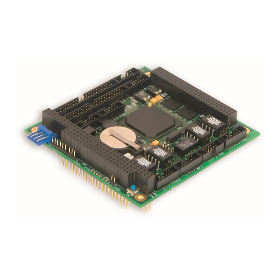
Page 1: User Manual
CPC307 PC/104-Plus Vortex86DX Based CPU Module User Manual Rev. 004 E April 2014... - Page 2 Product Title: CPC307 Document name: CPC307 User Manual Manual version: 003 E Ref. doc. v.: 3.2 R (467444 038) Copyright © 2014 Fastwel Co. Ltd. All rights reserved. Revision Record Rev. Index Brief Description of Changes Board Index Date of Issue Initial preliminary version CPC307 v 2.0...
-
Page 3: Table Of Contents
General Safety Precautions ............................. 6 Unpacking, Inspection and Handling ........................7 Three Year Warranty ............................... 8 Introduction ............................9 Module Introduction ............................9 CPC307 Versions ............................10 Delivery Checklist ............................11 Additional Accessories ..........................11 Technical Specifications ........................13 General ............................... 13 Power Requirements .......................... - Page 4 CPC307 3.2.16.3 FRAM ........................41 3.2.16.4 BIOS Upgrade......................41 3.2.17 Power Supply ..........................41 3.2.18 Power Supply Supervisor ......................42 3.2.19 GPIO Ports ..........................43 3.2.20 Configuration Jumpers ....................... 43 3.2.21 Diagnostic LEDs ........................43 3.2.22 Reset Button ..........................44 Address Mapping ............................
-
Page 5: List Of Tables
Table 3.21: XP5 Connector Pinout (CAN) ......................40 Table 3.22: XP22 Power Connector Pinout ......................42 Table 3.23: CPC307 Diagnostic LEDs Function ....................43 Table 3.24: XP3 Contacts Function ........................43 Table 3.25: Memory Address Mapping ....................... 44 Table 3.26: I/O Address Space .......................... -
Page 6: List Of Figures
This document contains information, which is property of Fastwel Co. Ltd. It is not allowed to reproduce it or transmit by any means, to translate the document or to convert it to any electronic form in full or in parts without antecedent written approval of Fastwel Co. Ltd. or one of its officially authorized agents. -
Page 7: Notation Conventions
CPC307 Notation Conventions Warning, ESD Sensitive Device! This symbol draws your attention to the information related to electro static sensitivity of your product and its components. To keep product safety and operability it is necessary to handle it with care and follow the ESD safety directions. -
Page 8: General Safety Precautions
However, prolonged operation near the maximum temperature is not recommended by Fastwel or by electronic chip manufacturers due to thermal stress related failure mechanisms. These mechanisms are common to all silicon devices, they can reduce the MTBF of the product by increasing the failure probability. -
Page 9: Unpacking, Inspection And Handling
If damage is observed (usually in the form of bent component leads or loose socketed components), contact Fastwel's official distributor from which you have purchased the product for additional instructions. Depending on the severity of the damage, the product may even need to be returned to the factory for repair. -
Page 10: Three Year Warranty
In performing all necessary installation and application operations, please follow only the instructions supplied by the present manual. In order to keep Fastwel’s warranty, you must not change or modify this product in any way, other than specifically approved by Fastwel or described in this manual. -
Page 11: Introduction
CPC307 Introduction This document presents general information on CPC307 CPU module, the details of its proper and safe installation, configuration and operation. The issues of PC/104 modules and external devices connection are also considered. This document applies to the module version 3.1. -
Page 12: Cpc307 Versions
Introduction CPC307 CPC307 Versions At the present time the CPC307 module is manufactured in several versions differing in interface capabilities. Table 1.1: CPC307 Versions Name CPC307-01 CPC307-02 CPC307-03 CPC307-04 CPC307-05 Processor Vortex86DX (600 MHz) 256 MB – Flash Disk 1 GB... -
Page 13: Delivery Checklist
Introduction CPC307 Delivery Checklist Table 1.2: CPC307 Supplied Set Name Description CPC30701 CPC307 processor module CPC30702 CPC30703 CPC30704 CPC30705 ACS00023 DB9F to IDC2-10 2 mm adapter cable for connection to COM port (685611.082) – Mounting standoffs kit – Jumpers set –... - Page 14 Introduction CPC307 Name Description ACS00048-04, Leotronics socket, 44 positions, 2 mm pitch and contacts set (ACS00049) or ACS00049, contacts with 1 m wires (ACS00049-02). Recommended counterpart for XP12 ACS00049-02 (LPT, USB), XP13 (IDE) headers of the module ACS00042 Null modem cable ACS00043-01 PS/2 cable.
-
Page 15: Technical Specifications
IDE port: One IDE channel (Primary) For CPC307-04: support for up to two UltraDMA-100 IDE devices if the microSD sockets are not populated For all other versions one IDE device can be connected Solid State Disk (except for CPC30704) ... - Page 16 COM5, COM6: RS422/485, up to 3.6 Mbaud, 500 V isolation (except for CPC307-03) Console operation via COM1 ... COM4 CAN: 2xCAN 2.0b (except for CPC307-03) SJA1000T controller Up to 1 Mbit/s 500 V isolation ...
-
Page 17: Power Requirements
XP22 (4-contact AMP 4-171826-4) power connector by an external DC power source. Power supply unit should provide starting current, which is 2.1 A for CPC307-02 version. It is allowed to use power supply units with current limiting not less than 1.2 A. Selecting a power supply unit, the starting current should be considered as well as the consumption current of expansion modules. -
Page 18: Dimensions And Weight
0.135 0.275 MTBF MTBF for CPC307 is 200000 hours. The value is calculated according to: Telcordia Issue 1 model, Method I Case 3, for continuous operation С. at a surface location, at normal environmental conditions and at ambient temperature 30 ©... -
Page 19: Functional Description
Functional Description CPC307 Functional Description Structure and Layout Functional diagram of the CPC307 module is shown in Figure 3.1. Figure 3.1: CPC307 Block Diagram PCI-104 Connector (PCI) ADM213E Isolated Addressing and DC/DC 500V Control Logic MAX1486 TSM0505S MAX3057 COM 1, 2... - Page 20 Real time clock with Li battery backup; CMOS+SFRAM (32 KB) for BIOS configuration storage; Layouts of main CPC307 components and connectors on top and bottom sides are presented in Figures 3.2 and 3.3 respectively. External connections are illustrated in Chapter ©...
-
Page 21: Figure 3.2: Top Side: Connectors And Main Components Layout
Functional Description CPC307 Figure 3.2: Top Side: Connectors and Main Components Layout HL1 HL2 CAN 1,2 COM3 COM4 XP13 XP12 XP10 XP14 XP11 COM1 GPIO XP15 XP16 XP17 COM2 LPT, XP18 COM 5,6 XP20 XP19 XP22 HL3 XP23 XP24 XP25... -
Page 22: Figure 3.3: Bottom Side: Connectors And Main Components Layout (Cpc30704)
Functional Description CPC307 Figure 3.3: Bottom Side: Connectors and Main Components Layout (CPC30704) microSD 0 microSD 1 The layout may slightly differ for various versions of the board. © 2 0 1 2 F a s t w e l v . -
Page 23: Functional Description
Functional Description CPC307 Functional Description 3.2.1 Vortex86DX SoC DM&P Vortex86DX includes the following main functional units: 32-bit х86 compatible core operating at 600 MHz; 32 KB L1, 256 KB L2 cache; Math coprocessor; 16-bit DDR2 SDRAM memory bus;... -
Page 24: Sdram Memory
No connection Two devices Important: Before connecting external devices to CPC307-04 make sure that no microSD slot is populated and “IDE” mode is selected for Primary IDE in BIOS Setup. Simultaneous connection of external IDE devices and microSD cards is not allowed. -
Page 25: Microsd
The operation modes of external IDE devices are set using jumpers on these devices. 3.2.4 MicroSD Two microSD cards can be connected to CPC307-04 using XS3 (channel 0) and XS4 (channel 1) sockets on the bottom side (Hirose DM3B-DSF-PEJ). Important: Before connecting microSD cards to CPC307-04 make sure that no external devices are connected to XP13 header and “SD”... -
Page 26: Ps/2 Keyboard And Mouse Interface
XP23 Connector Contacts Numbering To make a custom cable it is recommended to use as a counterpart connector Leotronics 2018-3061 socket with 2023-2000 contacts. The following table shows pinout of CPC307 XP23 connector. Table 3.4: XP23 Contacts Designation Pin Number... - Page 27 Functional Description CPC307 Depending on position of jumpers of XP25 pin header, the input is connected to different circuits: Closing contacts 1-2 of XP25 enables Reset on input; Closing contacts 4-5 of XP25 connects input to line 0 of GPIO1 port. Selection Reset function or IRQ line number is possible in BIOS Setup utility or by programming registers of GPIO1 port.
-
Page 28: Usb Interface
Functional Description CPC307 3.2.8 USB Interface The module is equipped with four USB 2.0 host ports routed to part of XP12 header contacts. Operation mode is selected in BIOS Setup. Each channel has separate power control and protection circuit (+5V, 500 mA). One USB device may be connected to each port. -
Page 29: Fast Ethernet Interface
3.2.9 Fast Ethernet Interface One Fast Ethernet channel (10/100 Mb/s) is available via XP9 connector on all versions of CPC307 except CPC30701. Ethernet controller is integrated in Vortex86DX SoC. Figure 3.11: XP9 Connector XP9 is a 2-row 2 mm pitch IDC10 header (Leotronics 2073-3102). -
Page 30: Table 3.7: Xp18 Pinpad Jumpers
Functional Description CPC307 RS485/422 Mode In RS485/422 mode transmitter is hardware controlled and receiver is constantly “on”. In RS485 mode (half duplex operation of RS485/422 converter) the lines TX+ and RX+ are connected in the driver, as well as TX- and RX- lines at the side of interface connector. In RS422 mode these lines are not connected and routed to the connector separately. -
Page 31: Table 3.8: Xp10 And Xp16 Pin Assignments
0.4A. It is not recommended to power more than one external module via interface connectors in order not to overload power circuits of CPC307. The following table shows pins designation for XP10 and XP16 headers. -
Page 32: Figure 3.15: Connection Of Several Devices In Rs422 Mode
Functional Description CPC307 Figure 3.15: Connection of Several Devices in RS422 Mode MASTER SLAVE SLAVE Figure 3.16: Connection of Several Devices in RS485 Mode MASTER SLAVE SLAVE © 2 0 1 2 F a s t w e l v . 0 0 3... -
Page 33: Com3 And Com4
+5V lines are protected by 0.5A fuse. Recommended consumption current for connected external modules is 0.4A. It is not recommended to power more than one external module via interface connectors in order not to overload power circuits of CPC307. Table 3.9: XP6 and XP7 Pin Assignments... -
Page 34: Table 3.11: Xp15 And Xp20 Pinpads Jumpers
Functional Description CPC307 Figure 3.17: XP15 and XP20 Pinpads XP15 XP20 120 (5%) ohm terminating resistors for RS485/422 1 2 3 4 1 2 3 4 modes can be connected by setting appropriate jumpers on XP15 and XP20 pinpads. Table 3.11:... -
Page 35: Parallel Printer Port (Lpt)
LPT port is available via first 26 contacts of XP12 2-row 2 mm pitch connector (IDC2-20 Leotronics 2073-3442). LPT port of CPC307 supports SPP, EPP, and ECP operation modes and has standard PC/AT base addresses. Base address and interrupt line are selected in BIOS Setup. -
Page 36: Expansion Buses: Isa And Pci
PC/104-Plus modules. Up to three PC/104-Plus PCI-master expansion modules are supported. Both connectors are available as a socket at the top side of the module and as a pin array with organizer at the bottom side of CPC307. 3.2.12.1 PCI Header PC/104-Plus standard specifies availability of 120-pin (30x4) 2 mm header. -
Page 37: Table 3.15: Xs1 Connector Contacts Designation (Rows C, D)
Functional Description CPC307 Signal State LC, mA Signal State LC, mA – Power AD16 In / Out – – – AD18 In / Out AD21 In / Out AD20 In / Out – – – AD23 In / Out –... -
Page 38: Isa Header
3.2.12.2 ISA Header XS2 header mounted on CPC307 allows connection of PC/104 expansion modules via ISA bus (8/16-bit, 8.3/16.6 MHz, DMA support). Master mode for peripheral modules is not supported. ISA signals are available both via the socket at the top side of the module (AMP 1375795-2) and via a pin array with organizer (AMP 1445251-1) at the bottom side of CPC307. -
Page 39: Table 3.17: Isa Xs2 (Rows C And D) Contacts Designation
Functional Description CPC307 Pin # Signal In/Out LC, mA Pin # Signal In/Out LC, mA /SMEMW SA19 /SMEMR SA18 /IOW SA17 /IOR SA16 /DACK3 – SA15 DRQ3 SA14 /DACK1 – SA13 DRQ1 SA12 /REFRESH SA11 BCLK – SA10 IRQ7 –... -
Page 40: Redundancy
3.2.13 Redundancy CPC307 supports redundancy connection. To do so, connect the main and the reserve modules in PC/104 stack with no connection via XS1 (PCI) connector. Make connection between XP1 and XP11 pinpads according to the figure below. -
Page 41: Can Ports
GPCS1# 3.2.14 CAN Ports Two independent CAN 2.0b interfaces of CPC307 are based on SJA1000T controllers. Both controllers can be reset by software. Base address (BA) selection is performed by programming registers of Vortex86DX SoC. Interrupt lines are hardware-defined. Maximum transmission rate for CAN1 and CAN2 ports is 1 Mbit/s. Both ports have 500 V isolation. -
Page 42: Watchdog Timers
3.2.16.1 Reserved BIOS The CPC307 takes advantage of flash-memory based BIOS. The main (working) copy of BIOS occupies 256 KB on a soldered chip. Reserve BIOS copy occupies 256 KB of flash memory integrated in the controller and is used for emergency boot. -
Page 43: Rtc, Cmos And Battery
3.2.16.2 RTC, CMOS and Battery The supplied with CPC307 3 V lithium battery (CR2032) is installed in X1 holder. It is used to power the RTC and CMOS memory when the system power is off. BIOS settings are duplicated to FRAM memory and are automatically recovered in case of CMOS data loss. -
Page 44: Power Supply Supervisor
3.2.18 Power Supply Supervisor CPC307 is equipped with ADM706T power supply supervisor. After +5V power is supplied to the module, ADM706T generates 200 ms Reset signal (Powergood signal is set to inactive “0” level), provided that the power voltage is higher than +3.08V. If during the operation +5V voltage drops below +4.45V, then PFO# (Power Fail Output) signal is generated. -
Page 45: Gpio Ports
Configuration Jumpers XP4, XP8, XP15, XP18, XP20, XP21, XP24, XP25, XP26, XP27 jumpers description (TBA). 3.2.21 Diagnostic LEDs CPC307 has three diagnostic LEDs (HL1, HL2, HL3). The following table describes the function of these LEDs. Table 3.23: CPC307 Diagnostic LEDs Function... -
Page 46: Reset Button
Functional Description CPC307 Figure 3.28: External LEDs Connection (XP3) 9 11 3.2.22 Reset Button In the event of a contingency (module hang-up, for example) use the Reset button SW1 on the top side of the module to reset the system. - Page 47 Functional Description CPC307 Address Range Function Note – 0065h WDT0 0066h ISA bus External bus access 0067h – 006Dh – WDT1 006Eh – 006Fh ISA bus External bus access 0070h – 007Fh – RTC, NMI Mask Register 0080h – 009Fh –...
-
Page 48: Integrated Address Decoder
Functional Description CPC307 3.3.3 Integrated Address Decoder Two SJA1000T CAN controllers and the controller of two RS232 ports (XR16C2850IM) require base addresses and address ranges to be set before use. For addressing these controllers two integrated in Vortex86DX address decoders are used: GPCS0 and GPCS1 (General Purpose Chip Select) lines. -
Page 49: Interrupt Settings
Functional Description CPC307 3.3.4 Interrupt Settings By default, interrupts are generated by the devices belonging to the CPC307 module. The table below presents interrupt settings. Interrupt request configuration is performed in BIOS Setup. Table 3.27: Interrupt Settings IRQ Lines System Units 10 11 12 13 14 15 ●... -
Page 50: Dma Channels
Functional Description CPC307 3.3.5 DMA Channels Table 3.28: DMA Channels LPT Port PC/104 Connector (ISA) ● DREQ0 ○ ● DREQ1 ○ ● DREQ2 ○ ● DREQ3 ● DREQ5 ● DREQ6 ● DREQ7 Legend: Not allowed ○ Possible ● Default Changes in the distribution of DMA requests are made by means of BIOS only. -
Page 51: Overall And Mounting Dimensions
Functional Description CPC307 Overall and Mounting Dimensions Figure 3.29: CPC307: Overall and Mounting Dimensions 73.7 11.1 90.6 © 2 0 1 2 F a s t w e l v . 0 0 3 C P C 3 0 7... -
Page 52: External Connections
Safety Regulations The following safety regulations must be observed when installing or operating the module. Fastwel assumes no responsibility for any damage resulting from infringement of these rules. Warning! When handling or operating the module, special attention should be paid to the heatsink, because it can get very hot during operation. -
Page 53: Connection Of Peripheral Devices
CPC307 Connection of Peripheral Devices Figure 4.1: External Devices Connection CPC307-05 v.3.0 The following devices are necessary to put the module into operation: PC/104 power supply or an external power supply unit with +5 V and not less than 2.1 A output connected to XP22 power connector;... -
Page 54: Ami Bios
CPC307 AMI BIOS The AMI BIOS in CPC307 is an adapted version of a standard BIOS for IBM PC AT-compatible personal computers equipped with x86 compatible processors. BIOS provides low-level support for the central processing, memory, and I/O system units. System settings can be changed using the BIOS Setup program. -
Page 55: Table 5.1: Main Menu Items
AMI BIOS CPC307 To start BIOS Setup, press "Del" key on a keyboard after the message "Hit <Del> if you want to run SETUP" appeared on the screen. This will lead you to the Main Menu screen, shown in the Figure below. -
Page 56: Advanced
AMI BIOS CPC307 Use "Up" and "Down" cursor keys or <Tab> key to move between menu items. <Enter> selects the item and allows to proceed with the command or opens the submenu screen. Advanced On selection of this Main menu item the following screen is shown: Figure 5.2:... -
Page 57: Cpu Configuration
AMI BIOS CPC307 5.3.1 CPU Configuration The menu screen is shown in the figure below. Figure 5.3: CPU Configuration Menu Screen The figure shows the default settings. Table 5.3: CPU Configuration Menu Items Menu Item Options Description CPU Configuration CPU information: (info field) Brand String –... -
Page 58: Ide Configuration
[Legacy Mode] IDE controller operation mode [Native Mode] Primary IDE Pin Select [SD Card] SD card mode support enabled; (available for CPC307-04 only) [Parallel IDE] IDE devices operation supported Primary IDE Master Primary IDE Master device: information and settings (подменю) Primary IDE Slave Primary IDE Slave device: information and settings. -
Page 59: Table 5.5: Primary Ide Master Menu Items
AMI BIOS CPC307 Menu Item Options Description ATA(PI) 80Pin Cable Detection [Host & Device] Detection by system and IDE devices; [Host] Detection by system only; [Device] Detection by IDE devices only. In Native mode of IDE controller this may lead to data loss on the integrated ATA Flash disk Primary IDE Master/Slave Primary IDE Master and Primary IDE Slave submenus are identical by structure. -
Page 60: Remote Access Configuration
AMI BIOS CPC307 Menu Item Options Description PIO Mode [Auto] BIOS auto detects if the connected device supports PIO mode. Recommended if the supported mode is unknown. Sets PIO 0 mode. Data transfer rate is up to 3.3 MB/s; PIO 1 mode. DTR up to 5.2 MB/s;... -
Page 61: Table 5.6: Remote Access Configuration Menu Items
AMI BIOS CPC307 Table 5.6: Remote Access Configuration Menu Items Menu Item Options Description Remote Access [Disabled] Remote access disabled; [Enabled] Remote access enabled. Remote access parameters become available for editing. Serial port number [COM1] Selection of a serial port for remote access... -
Page 62: Usb Configuration
AMI BIOS CPC307 5.3.4 USB Configuration The menu screen is shown in the figure below. Figure 5.7: USB Configuration Menu Screen The figure shows the default settings. Table 5.7: Name Menu Item Options Description Legacy USB Support [Disabled] Legacy support disabled [Enabled] Support enabled. -
Page 63: Pci Plug And Play
AMI BIOS CPC307 PCI Plug and Play PCI Plug and Play menu screen is shown on the following figure: Figure 5.8: PCI Plug and Play Menu Screen The figure shows the default settings. PCI Plug and Play menu items are described in the table below. - Page 64 AMI BIOS CPC307 Menu Item Options Description [32], [64], [96], Maximum number of PCI bus clocks that a device on bus can keep PCI Latency Timer [128], [160], it busy sending data. [192], [224], [248] [No] Do not allow to assign an interrupt to PCI graphics card...
-
Page 65: Boot Options
AMI BIOS CPC307 Boot Options Boot menu screen is shown on the following figure: Figure 5.9: Boot Menu Screen The figure shows the default settings. Boot menu items are described in the table below. Table 5.9: Boot Menu Items Menu Item... -
Page 66: Boot Settings Configuration
AMI BIOS CPC307 5.5.1 Boot Settings Configuration The menu screen is shown in the figure below. Figure 5.10: Boot Settings Configuration Menu Screen The figure shows the default settings. Table 5.10: Boot Settings Configuration Menu Items Menu Item Options Description... -
Page 67: Security Options
AMI BIOS CPC307 Security Options Security menu screen is shown on the following figure: Figure 5.11: Security Menu Screen Table 5.11: Security Menu Items Menu Item Options Description Change Supervisor Password Password for loading the system. It is requested during POST... -
Page 68: Chipset Menu
AMI BIOS CPC307 Chipset Menu The menu screen is shown in the figure below. Figure 5.12: Chipset Menu Screen Image The figure shows the default settings. Table 5.12: Chipset Menu Items Menu Item Options Description NorthBridge Configuration Access to North bridge settings (see below) -
Page 69: North Bridge Configuration
AMI BIOS CPC307 5.7.1 North Bridge Configuration The menu screen is shown in the figure below. Figure 5.13: North Bridge Configuration Menu Screen Table 5.13: North Bridge Configuration Menu Items Menu Item Options Description CPU Speed Setting [Devide by 1] Recommended setting for clock divider;... -
Page 70: South Bridge Configuration
AMI BIOS CPC307 5.7.2 South Bridge Configuration The menu screen is shown in the figure below. Figure 5.14: South Bridge Configuration Menu Screen Table 5.14: South Bridge Configuration Menu Items Menu Item Options Description USB Port 0,1 [Enabled] USB ports 0 and 1 control... -
Page 71: Exit Menu
AMI BIOS CPC307 Menu Item Options Description CAN and COM5,6 Settings for CAN1,2 and COM5,6 ports (TBA) Configuration (submenu) Exit Menu The figure below presents the Exit menu screen. Figure 5.15: Exit Menu Screen Image Table 5.15: Exit Menu Items... -
Page 72: Functional Constraints Of Bios Versions
AMI BIOS CPC307 Functional Constraints of BIOS Versions BIOS v.3.12 (Core Version 8.00.15, created 31/01/2012) preinstalled in version 3.1 modules, has the following functional constraints: Corrected skipping of Autoexec.bat at the command Ctrl+B from a remote PC. Corrected remote operation via COM2. -
Page 73: Annex A: Bios Update
(due to power loss, downloading of invalid BIOS image file etc.). Relevant BIOS image file versions for CPC307 module can be downloaded from the following link: ftp://ftp.prosoft.ru/pub/Hardware/Fastwel/CPx/CPC307/ The BIOS primary copy is stored in the chip of parallel FLASH-memory, connected to ISA bus - AM29F040B-55EF memory chip, 4 Mb Flash Memory. - Page 74 1. Install XP21 jumper, and not to install XP26 jumper. Otherwise, it is impossible to update the backup copy. 2. Switch on CPC307 and boot it in the standard mode from BIOS primary copy. WDT2 watchdog timer should not be actuated during the booting process (p. 4.3.16.2 WDT2 watchdog timer). Make sure that the WDT2 watchdog timer was not actuated;...
- Page 75 1. Install XP21 jumper and remove XP26 jumper. 2. Switch on CPC307 and boot the module from BIOS backup copy (if BIOS primary copy is damaged, WDT2 watchdog timer will be actuated). After the module’s reboot, optimal (factory) BIOS Setup settings can be loaded. If necessary, you should enter BIOS Setup, change the required parameters, save the changes and exit (p.
Need help?
Do you have a question about the CPC307 and is the answer not in the manual?
Questions and answers