
Fastwel CPC307 Series Manuals
Manuals and User Guides for Fastwel CPC307 Series. We have 3 Fastwel CPC307 Series manuals available for free PDF download: User Manual
Fastwel CPC307 Series User Manual (117 pages)
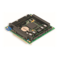
PC/104-Plus Vortex86DX Based CPU Module
Brand: Fastwel
|
Category: Control Unit
|
Size: 4.96 MB
Table of Contents
-
Introduction11
-
Mechanical18
-
Mtbf21
-
DDR2 Memory38
-
Microsd41
-
Serial Ports45
-
GPIO Ports77
-
Leds84
-
Main87
-
Advanced88
-
Pcipnp97
-
Boot99
-
Security102
-
Chipset103
-
Exit112
Advertisement

Fastwel CPC307 Series User Manual (113 pages)
PC/104-Plus Vortex86DX Based CPU Module
Brand: Fastwel
|
Category: Control Unit
|
Size: 4.22 MB
Table of Contents
-
-
General15
-
Mechanical17
-
Mtbf20
-
-
-
-
-
DDR2 Memory37
-
Microsd39
-
Serial Ports44
-
GPIO Ports75
-

Fastwel CPC307 Series User Manual (75 pages)
PC/104-Plus Vortex86DX Based CPU Module
Brand: Fastwel
|
Category: Motherboard
|
Size: 2.84 MB
Table of Contents
-
-
-
SDRAM Memory24
-
Microsd25
-
Serial Ports29
-
-
PCI Header36
-
ISA Header38
-
-
Redundancy40
-
CAN Ports41
-
Power Supply43
-
GPIO Ports45
-
Reset Button46
-
-
DMA Channels50
-
5 Ami Bios
54-
Main Menu54
-
Advanced56
-
Boot Options65
-
Chipset Menu68
-
Exit Menu71
Advertisement