Sony HCD-FX80 Service Manual
Hide thumbs
Also See for HCD-FX80:
- Operating instructions manual (104 pages) ,
- Supplementary manual (1 page)
Table of Contents
Advertisement
Quick Links
QQ
3 7 63 1515 0
SERVICE MANUAL
Ver. 1.2 2005.12
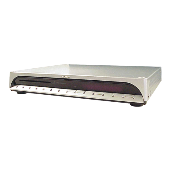
HCD-FX80 is the amplifier, DVD/CD and
tuner section in DAV-FX80.
This system incorporates with Dolby*1 Digital and
Dolby Pro Logic (II) adaptive matrix surround decoder
and the DTS*2 Digital Surround System.
*1 Manufactured under license from Dolby Laboratories.
"Dolby," "Pro Logic," and the double-D symbol are trademarks
of Dolby Laboratories.
*2 Manufactured under license from Digital Theater Systems, Inc.
TE
L 13942296513
"DTS" and "DTS Digital Surround" are trademarks of Digital
Theater Systems, Inc.
AUDIO POWER SPECIFICATIONS
POWER OUTPUT AND
TOTAL HARMONIC
DISTORTION:
Amplifier section
Surround mode (reference) music power output
www
.
Sony Corporation
9-879-687-03
Home Audio Division
2005L16-1
Published by Sony Engineering Corporation
© 2005.12
http://www.xiaoyu163.com
* Depending on the sound field settings and the source,
there may be no sound output.
Inputs (Analog)
With 3 ohm loads, both
VIDEO 1, VIDEO 2
channels driven, from
200 – 20,000 Hz; rated
Inputs (Digital)
55 watts per channel
VIDEO 1 (Coaxial)
minimum RMS power,
VIDEO 2 (Optical)
with no more than 0.7 %
Phones
total harmonic distortion
from 250 milli watts to
rated output.
Super Audio CD/DVD system
Laser
Front: 143 W + 143 W
(with SS-TS46)
Center*: 143 W
(with SS-CT46)
Signal format system
Surround*: 143 W + 143
Frequency response (at 2 CH STEREO mode)
W
(with SS-TS43B)
Subwoofer*: 285 W
(with SS-WS42)
x
ao
y
i
http://www.xiaoyu163.com
HCD-FX80
8
Model Name Using Similar Mechanism
Mechanism Type
Optical Pick-up Name
Q Q
3
6 7
1 3
SPECIFICATIONS
Sensitivity: 450 mV
Impedance: 50 kilohms
Impedance: 75 ohms
Accepts low-and high-
impedance headphones.
Semiconductor laser
(Super Audio CD/DVD:
= 650 nm)
λ
(CD:
= 790 nm)
Emission duration:
continuous
NTSC
DVD (PCM): 2 Hz to 22
kHz (±1.0 dB)
CD: 2 Hz to 20 kHz (±1.0
dB)
u163
.
2 9
9 4
2 8
Canadian Model
HCD-FX10
CDM69EH-DVBU101
KHM-310CAB/C2NP
1 5
0 5
8
2 9
9 4
Tuner section
System
PLL quartz-locked digital
synthesizer system
FM tuner section
Tuning range
87.5 – 108.0 MHz
(100 kHz step)
Antenna (aerial)
FM wire antenna (aerial)
Antenna (aerial) terminals 75 ohms, unbalanced
Intermediate frequency
10.7 MHz
AM tuner section
Tuning range
530 – 1,710 kHz (with the
interval set at 10 kHz)
531 – 1,710 kHz (with the
interval set at 9 kHz)
λ
Antenna (aerial)
AM loop antenna (aerial)
Intermediate frequency
450 kHz
— Continued on next page —
m
DVD RECEIVER
co
9 9
US Model
2 8
9 9
Advertisement
Table of Contents

Related Manuals for Sony HCD-FX80


Summary of Contents for Sony HCD-FX80
- Page 1 3 7 63 1515 0 SERVICE MANUAL US Model Canadian Model Ver. 1.2 2005.12 HCD-FX80 is the amplifier, DVD/CD and tuner section in DAV-FX80. This system incorporates with Dolby*1 Digital and Model Name Using Similar Mechanism HCD-FX10 Dolby Pro Logic (II) adaptive matrix surround decoder...
- Page 2 LES DIAGRAMMES SCHÉMATIQUES ET LA LISTE DES PIÈCES SONT CRITIQUES POUR LA SÉCURITÉ DE FONCTIONNEMENT. NE REMPLACER CES COM- POSANTS QUE PAR DES PIÈCES SONY DONT LES NUMÉROS SONT DONNÉS DANS CE MANUEL OU DANS LES SUPPLÉMENTS PUBLIÉS PAR SONY.
- Page 3 HCD-FX80 3 7 63 1515 0 Laser component in this product is capable of emitting radiation exceeding the limit for Class 1. This appliance is classified as a CLASS 1 LASER product. The CLASS 1 LASER PRODUCT MARKING is located on the bottom exterior.
-
Page 4: Table Of Contents
HCD-FX80 3 7 63 1515 0 TABLE OF CONTENTS SERVICING NOTE 7-6. Schematic Diagram – DMB10 Section (1/4) – ....38 ........... 5 7-7. Schematic Diagram – DMB10 Section (2/4) – ....39 7-8. Schematic Diagram – DMB10 Section (3/4) – ....40 GENERAL .............. -
Page 5: Servicing Note
To prevent a malfunction, the system has performed the self- (xx is a number) diagnosis function. u163 ,Contact your nearest Sony dealer or local authorized Sony service facility and give the 5- character service number. Example: E 61 10 http://www.xiaoyu163.com... -
Page 6: General
HCD-FX80 SECTION 2 This section is extracted from instruction manual. 3 7 63 1515 0 GENERAL Front panel A Disc slot (36) H x (stop) (37, 76) I X (pause) (37) (remote sensor) (13) C Front panel display (96) - Page 7 HCD-FX80 3 7 63 1515 0 F TOP MENU (41) Remote G C/X/x/c/ENTER (32, 38, 50, 60, 63, 65, 72, 77) C/X/x/c have tactile dots.* H O RETURN (43) I ALBUM –/+ (37, 70) J ANGLE (64) K AUDIO (58) The AUDIO button has a tactile dot.*...
-
Page 8: Disassembly
HCD-FX80 SECTION 3 3 7 63 1515 0 DISASSEMBLY 3-1. DISASSEMBLY FLOW • This set can be disassembled in the order shown below. • The dotted square with arrow ( ) prompts you to move to the next job when all of the works within the dotted square ( ) are completed. -
Page 9: Top Panel Sub Assy
HCD-FX80 3 7 63 1515 0 Note: Follow the disassembly procedure in the numerical order given. 3-2. TOP PANEL SUB ASSY top panel sub assy 2 two flat head screws (TP) 1 two flat head screws (TP) 4 three screws 3 ×... -
Page 10: Front Panel Assy
HCD-FX80 3 7 63 1515 0 3-3. FRONT PANEL ASSY 2 three screws 3 × 8) (+BVTP MD cover screw 3 × 8) (+BVTP 4 wire (flat type) 19p(CN801) screw 3 × 8) (+BVTP front panel assy L 13942296513... -
Page 11: Mib01 Board, Mib01 Power Board
HCD-FX80 3 7 63 1515 0 3-5. MIB01 BOARD, MIB01 POWER BOARD 1 two screws (+BV 3) 5 wire (flat type) 4 MIB01 POWER board 13p(CN5301) 2 connector (CN9002) 3 connector (CN9001) 7 two screws (+BVTP 3 × 8) -
Page 12: Main Board, H/P Board
HCD-FX80 3 7 63 1515 0 3-7. MAIN BOARD, H/P BOARD 9 two screws 7 wire (flat type) (+BV 23p(CN507) screw 8 wire (flat type) 3 × 14) (+BVTP 11p(CN504) 6 wire (flat type) 27p(CN502) heat sink 5 wire (flat type) -
Page 13: Dvd Mechanism Deck (Cdm69Eh-Dvbu101)
HCD-FX80 3 7 63 1515 0 3-9. DVD MECHANISM DECK (CDM69EH-DVBU101) 3 DVD mechanism deck (CDM69EH-DVBU101) 1 two screws 2 two screws (+BV (+BV L 13942296513 3-10. BASE UNIT (DVBU101) 1 floating screw (DIA. 12) 2 boss u163 5 boss... -
Page 14: Optical Pick-Up (Khm-310Cab/C2Np)
HCD-FX80 3 7 63 1515 0 3-11. OPTICAL PICK-UP (KHM-310CAB/C2NP) 3 insulator screw optical pick-up (KHM-310CAB/C2NP) 8 insulator 2 insulator screw 4 insulator screw 7 insulator 9 insulator 1 insulator screw 6 insulator L 13942296513 3-12. SW BOARD, BRACKET (TOP) ASSY... -
Page 15: Relay Board
HCD-FX80 3 7 63 1515 0 3-13. RELAY BOARD 4 connector (CN710) – bottom view – 5 connector (CN703) RELAY board 2 four screws (+BVTP2.6) 6 RELAY board L 13942296513 1 Remove five solders. 3-14. MOTOR (STOCKER) ASSY (STOCKER)(M761) 3 two screws (+BVTP2.6) -
Page 16: Motor (Roller) Assy (Roller)(M781)
HCD-FX80 3 7 63 1515 0 3-15. MOTOR (ROLLER) ASSY (ROLLER)(M781) 3 two screws (+BVTP2.6) 2 Remove two solders. 4 ROLLER MOTOR board 5 motor (roller) assy (roller)(M781) 1 belt (roller V) L 13942296513 3-16. MOTOR (MODE) ASSY (MODE)(M771) 3 two screws (+BVTP2.6) -
Page 17: Rubber Roller (Slider) Assy
HCD-FX80 3 7 63 1515 0 3-17. RUBBER ROLLER (SLIDER) ASSY 5 step screw 8 step screw 1 step screw 9 tension 7 rubber roller spring 0 rubber roller (slider 1) assy (slider 2) (slider 4) assy 2 rubber roller... -
Page 18: Cam (Gear)
HCD-FX80 3 7 63 1515 0 3-19. CAM (GEAR) qf cam (gear) : Note 6 gear (mode 5) qd screw 5 screw (PTPWH2.6 × 8) 4 gear (mode 5) qs gear(mode cam) 3 screw (PTPWH2.6 × 8) qa screw (PTPWH2.6 ×... -
Page 19: Assembly
HCD-FX80 SECTION 4 3 7 63 1515 0 ASSEMBLY • This set can be assembled in the order shown below. 4-1. HOW TO INSTALL THE CAM (EJECT LOCK) 1 Rotate the cam (BU U/D) fully in the direction of arrow. -
Page 20: How To Install The Gear (Mode C)
HCD-FX80 3 7 63 1515 0 4-3. HOW TO INSTALL THE GEAR (MODE C) 1 Align the mark on the rotary encoder (S771) with the projection of the assy. 2 Check that the cam (BU U/D) can not be rotated in the direction of arrow. -
Page 21: How To Install The Rotary Encorder (S702)
HCD-FX80 3 7 63 1515 0 4-5. HOW TO INSTALL THE ROTARY ENCORDER (S702), GEAR (STOCKER COMMUNICATION) 4 gear 5 screw (PTPWH2.6 × 8) (stocker communication) 3 screw 7 two screws (PWH2 × 6) (PTPWH2.6 × 8) 1 rotary encoder... -
Page 22: Test Mode
HCD-FX80 SECTION 5 3 7 63 1515 0 TEST MODE 3. Disc Tray Lock Note 1: Regarding the notification symbol “R” The disc tray lock function for the antitheft of an demonstration Because the number of the operating buttons of this product disc in the store is equipped. - Page 23 HCD-FX80 Ver. 1.1 3 7 63 1515 0 4-4. MIRROR TIME ADJUSTMENT DVD SECTION [TEST DISC LIST] To enter Mirror Time Adjustment, press 5 “R” button on the remote Be sure to use the DVD disc that matches the signal standards of commander.
- Page 24 HCD-FX80 3 7 63 1515 0 (3) Select “5. MIRR time Adjust”. (14) Confirm the same values are displayed. If it is not same, return to step 7. Drive Manual Operation MIRR time Adjust Menu 1. Servo Control 2. Track/Layer Jump 1.
- Page 25 HCD-FX80 3 7 63 1515 0 4-5. EXECUTING IOP MEASUREMENT (5) Wait until a hexadecimal number appear. Manual Adjust In order to execute mirror time adjustment, the following standard procedures must be followed. 1. Track Balance Adjust: 2. Track Gain Adjust: (1) In standby mode, press three buttons x , A and 3.
-
Page 26: Electrical Adjustment
HCD-FX80 SECTION 6 3 7 63 1515 0 ELECTRICAL ADJUSTMENT 2. Component Output Level Adjustment (MIB01 Board) HDMI SECTION <Purpose> This adjusts component output level. If it is incorrect, correct ADJUSTMENT OF VIDEO SYSTEM brightness will not be attained when connected to, for instance, projector. -
Page 27: Diagrams
HCD-FX80 SECTION 7 3 7 6 3 1 5 1 5 0 DIAGRAMS • Circuit Boards Location THIS NOTE IS COMMON FOR PRINTED WIRING BOARDS AND SCHEMATIC DIAGRAMS. (In addition to this, the necessary note is printed in each block.) For Schematic Diagrams. -
Page 28: Block Diagram - Rf Section
HCD-FX80 7-1. BLOCK DIAGRAM – RF SECTION – 3 7 6 3 1 5 1 5 0 • Signal Path : CD PLAY YUV0 YUV0 DVDRFIP : DVD PLAY YUV1 YUV1 YUV2 : SACD PLAY YUV2 YUV3 YUV3 : AUDIO... -
Page 29: Mib Section
HCD-FX80 – MIB SECTION – 3 7 6 3 1 5 1 5 0 PO2 - PO9 Signal Pash : VIDEO 53-55, 58-62 S(2) - S(9) 33 RESET8 : CHROMA 49 S_VSYNC : COMPONENT VIDEO VIDEO 50 S_HSYNC SECTION... -
Page 30: Video Section
HCD-FX80 – VIDEO SECTION – 3 7 6 3 1 5 1 5 0 J601(1/2) VIDEO1 VIDEO IN VIDEO2 VIDEO IN IC201 IC204 VIDEO AMP, 75Ω DRIVER VIDEO SWITCH 14 2B OUT2 6 YIN YOUT S VIDEO(DVD ONLY) OUT3... -
Page 31: Amp Section
HCD-FX80 – AMP SECTION – 3 7 6 3 1 5 1 5 0 ALRCK ABCK ASDATA0 ASDATA1 ASDATA2 IC506 IC507 DIGITAL AUDIO SD-RAM PROCESSOR SECTION (Page 28) 7-10 72-75 13-16 77-80 18-21 D0-D15 98,99 D0 – D15 24,25... -
Page 32: Audio Section
HCD-FX80 – AUDIO SECTION – 3 7 6 3 1 5 1 5 0 IC301 IC108 HEADPHONE STREAM PROCESSOR J801 HPOUTL1 PHONES HPOUTL2 • Signal Path Q507 : AUDIO HPOUTR1 Q806 - 809 MUTING MUTING HPOUTR2 CONTROL IC101 SPEAKER POWER DRIVER D1 –... -
Page 33: Main Section
HCD-FX80 – MAIN SECTION – 3 7 6 3 1 5 1 5 0 IC721 STOCKER MOTOR DRIVE OUT1 M761 (STOCKER) OUT2 IC711 ROLLER MOTOR DRIVE OUT1 M781 OUT2 (ROLLER) IC701 MODE MOTOR DRIVE OUT1 DC/DC M771 OUT2 (MODE) -
Page 34: Printed Wiring Board - Changer Section
HCD-FX80 • See page 27 for Circuit Boards Location. 7-2. PRINTED WIRING BOARD – CHANGER SECTION – :Uses unleaded solder. 3 7 6 3 1 5 1 5 0 SW(1) BOARD RELAY BOARD MAIN BOARD CN502 (Page 42) SW(2) BOARD... -
Page 35: Schematic Diagram - Changer Section
HCD-FX80 • See page 66 for IC Block Diagrams. 7-3. SCHEMATIC DIAGRAM – CHANGER SECTION – 3 7 6 3 1 5 1 5 0 RELAY BOARD CN751 CN702 R731 DIODE DIODE I C 7 5 1 D SENSE... -
Page 36: Printed Wiring Board - Dmb10 Section (Side A)
HCD-FX80 • See page 27 for Circuit Boards Location. 7-4. PRINTED WIRING BOARD – DMB10 SECTION (SIDE A) – :Uses unleaded solder. 3 7 6 3 1 5 1 5 0 IC103 (EEP ROM) can not be replaced individually. -
Page 37: Printed Wiring Board - Dmb10 Section (Side B)
HCD-FX80 • See page 27 for Circuit Boards Location. 7-5. PRINTED WIRING BOARD – DMB10 SECTION (SIDE B) – :Uses unleaded solder. 3 7 6 3 1 5 1 5 0 • Semiconductor Location Ref. No. Location IC105 IC107... -
Page 38: Schematic Diagram - Dmb10 Section (1/4)
HCD-FX80 7-6. SCHEMATIC DIAGRAM – DMB10 SECTION (1/4) – 3 7 6 3 1 5 1 5 0 FL401 CN401 FB402 FB404 JL4601 JL4602 FL403 JL4603 JL4604 FB403 FB406 JL4605 JL4606 JL4607 JL4608 (Page 39, C402 C403 MAIN JL4609 JL4610 6.3V... -
Page 39: Schematic Diagram - Dmb10 Section (2/4)
HCD-FX80 • See page 75 for IC Pin Function Description. • See page 65 for Waveforms. 7-7. SCHEMATIC DIAGRAM – DMB10 SECTION (2/4) – 3 7 6 3 1 5 1 5 0 (Page 40) (Page 38) (Page 38) -
Page 40: Schematic Diagram - Dmb10 Section (3/4)
HCD-FX80 7-8. SCHEMATIC DIAGRAM – DMB10 SECTION (3/4) – 3 7 6 3 1 5 1 5 0 IC103 (EEP ROM) can not be replaced individually. Replace it with DMB10 board assembly for service. (Page 39) (Page 39) C181... -
Page 41: Schematic Diagram - Dmb10 Section (4/4)
HCD-FX80 7-9. SCHEMATIC DIAGRAM – DMB10 SECTION (4/4) – 3 7 6 3 1 5 1 5 0 (Page 39) (Page 38, 39, 40) R225 R223 100k 100k R232 R234 R231 R221 C211 0.033 C209 R230 C233 0.033 0.0047... -
Page 42: Printed Wiring Board - Main Section (Side A)
HCD-FX80 7-10. PRINTED WIRING BOARD – MAIN SECTION (SIDE A) – HCD-FX80... -
Page 43: Printed Wiring Board - Main Section (Side B)
HCD-FX80 • See page 27 for Circuit Boards Location. 7-11. PRINTED WIRING BOARD – MAIN SECTION (SIDE B) – :Uses unleaded solder. 3 7 6 3 1 5 1 5 0 SPEAKER FRONT:ONLY FOR SS-TS46 SURROUND:ONLY FOR SS-TS43B • Semiconductor... -
Page 44: Schematic Diagram - Main Section (1/8)
HCD-FX80 • See page 72 for IC Pin Function Description. • See page 65 for Waveform. 7-12. SCHEMATIC DIAGRAM – MAIN SECTION (1/8) – 3 7 6 3 1 5 1 5 0 CN509 FFC-S-1.0 ( 1 / 8 ) -
Page 45: Schematic Diagram - Main Section (2/8)
HCD-FX80 7-13. SCHEMATIC DIAGRAM – MAIN SECTION (2/8) – 3 7 6 3 1 5 1 5 0 MAIN BOARD (1/8) (Page 44) IC515 ( 2 / 8 ) IC TA7809LS TP517 C595 C596 C597 R704 47 35V 0.33... -
Page 46: Schematic Diagram - Main Section (3/8)
HCD-FX80 • See page 67 for IC Block Diagrams. 7-14. SCHEMATIC DIAGRAM – MAIN SECTION (3/8) – 3 7 6 3 1 5 1 5 0 ( 3 / 8 ) R345 R468 R347 R469 EB910 TERMINAL BOARD TP331... -
Page 47: Schematic Diagram - Main Section (4/8)
HCD-FX80 • See page 67 for IC Block Diagrams. 7-15. SCHEMATIC DIAGRAM – MAIN SECTION (4/8) – 3 7 6 3 1 5 1 5 0 ( 4 / 8 ) R384 R480 R383 C137 IC106 R120 R128 25V F... -
Page 48: Schematic Diagram - Main Section (5/8)
HCD-FX80 • See page 67 for IC Block Diagram. • See page 65 for Waveform. 7-16. SCHEMATIC DIAGRAM – MAIN SECTION (5/8) – 3 7 6 3 1 5 1 5 0 MAIN BOARD (3/8) (Page 46) ( 5 / 8 ) -
Page 49: Schematic Diagram - Main Section (6/8)
HCD-FX80 • See page 67 for IC Block Diagrams. 7-17. SCHEMATIC DIAGRAM – MAIN SECTION (6/8) – 3 7 6 3 1 5 1 5 0 MAIN BOARD (4/8) (Page 47) ( 6 / 8 ) IC103 Q106 Q108... -
Page 50: Schematic Diagram - Main Section (7/8)
HCD-FX80 7-18. SCHEMATIC DIAGRAM – MAIN SECTION (7/8) – 3 7 6 3 1 5 1 5 0 ( 7 / 8 ) MAIN BOARD (6/8) C938 D931 YG906C2R (Page 49) 330P CN901 FH901 FH902 C963 HOLDER HOLDER 680P... -
Page 51: Schematic Diagram - Main Section (8/8)
HCD-FX80 • See page 70 for IC Pin Function Description. • See page 66, 68 for IC Block Diagrams. • See page 65 for Waveform. 7-19. SCHEMATIC DIAGRAM – MAIN SECTION (8/8) – 3 7 6 3 1 5 1 5 0... -
Page 52: Printed Wiring Board - Fl/Key Section
HCD-FX80 • See page 27 for Circuit Boards Location. 7-20. PRINTED WIRING BOARD – FL/KEY SECTION – :Uses unleaded solder. 3 7 6 3 1 5 1 5 0 • Semiconductor Location Ref. No. Location D801 D802 D803 D804... -
Page 53: Schematic Diagram - Fl/Key Section
HCD-FX80 • See page 66 for IC Block Diagrams. 7-21. SCHEMATIC DIAGRAM – FL/KEY SECTION – 3 7 6 3 1 5 1 5 0 R852 R855 R857 R858 R851 R853 R856 2.2k 2.2k 4.7k 2.2k 4.7k 2.2k TP833... -
Page 54: Printed Wiring Board - Led / H/P Section
HCD-FX80 • See page 27 for Circuit Boards Location. 7-22. PRINTED WIRING BOARD – LED / H/P SECTION – :Uses unleaded solder. 3 7 6 3 1 5 1 5 0 • Semiconductor Location Ref. No. Location D811 PHONES... -
Page 55: Schematic Diagram - Led / H/P Section
HCD-FX80 7-23. SCHEMATIC DIAGRAM – LED / H/P SECTION – 3 7 6 3 1 5 1 5 0 R833 R867 TP843 4.7k R834 R835 R836 R837 R838 R839 R863 R866 TP841 2.2k 2.2k 4.7k L813 CN803 S815 S809... -
Page 56: Printed Wiring Board - I/O Section (Side A)
HCD-FX80 • See page 27 for Circuit Boards Location. 7-24. PRINTED WIRING BOARD – I/O SECTION (SIDE A) – :Uses unleaded solder. 3 7 6 3 1 5 1 5 0 • Semiconductor Location Ref. No. Location IC201 IC203... -
Page 57: Printed Wiring Board - I/O Section (Side B)
HCD-FX80 • See page 27 for Circuit Boards Location. 7-25. PRINTED WIRING BOARD – I/O SECTION (SIDE B) – :Uses unleaded solder. 3 7 6 3 1 5 1 5 0 AUDIO IN MONITOR VIDEO 1 VIDEO IN COMPONENT... -
Page 58: Schematic Diagram - I/O Section
HCD-FX80 • See page 69 for IC Block Diagrams. • See page 65 for Waveform. 7-26. SCHEMATIC DIAGRAM – I/O SECTION – 3 7 6 3 1 5 1 5 0 CN101 R659 TP626 TP625 TP627 L601 IC603 TORX141L... -
Page 59: Printed Wiring Board - Mib01 Section (Side A)
HCD-FX80 • See page 27 for Circuit Boards Location. 7-27. PRINTED WIRING BOARD – MIB01 SECTION (SIDE A) – :Uses unleaded solder. 3 7 6 3 1 5 1 5 0 CN601 HD MI (DVD ONLY) • Semiconductor Location Ref. -
Page 60: Printed Wiring Board - Mib01 Section (Side B)
HCD-FX80 • See page 27 for Circuit Boards Location. 7-28. PRINTED WIRING BOARD – MIB01 SECTION (SIDE B) – :Uses unleaded solder. 3 7 6 3 1 5 1 5 0 • Semiconductor Location Ref. No. Location IC111 IC505... -
Page 61: Schematic Diagram - Mib01 Section (1/3)
HCD-FX80 • See page 80 for IC Pin Function Description. 7-29. SCHEMATIC DIAGRAM – MIB01 SECTION (1/3) – 3 7 6 3 1 5 1 5 0 IC509 HY57V161610ETP-7 CL502 C516 0.01 R5452 4.7k C520 C512 C505 C513 6.3V 6.3V... -
Page 62: Schematic Diagram - Mib01 Section (2/3)
HCD-FX80 • See page 83 for IC Pin Function Description. 7-30. SCHEMATIC DIAGRAM – MIB01 SECTION (2/3) – 3 7 6 3 1 5 1 5 0 C543 0.033 JL501 R527 R509 C541 R526 3.3k 0.33 C536 C539 C540... -
Page 63: Schematic Diagram - Mib01 Section (3/3)
HCD-FX80 • See page 65 for Waveform. 7-31. SCHEMATIC DIAGRAM – MIB01 SECTION (3/3) – 3 7 6 3 1 5 1 5 0 R696 C627 0.01 C620 0.01 R612 R664 C611 0.01 R690 C607 0.01 C625 C629 C621 C623 0.22... -
Page 64: Printed Wiring Board - Mib01 Power Section
HCD-FX80 7-32. PRINTED WIRING BOARD – MIB01 POWER SECTION – 7-33. SCHEMATIC DIAGRAM – MIB01 POWER SECTION – 3 7 6 3 1 5 1 5 0 • See page 27 for Circuit Boards Location. :Uses unleaded solder. IC901... - Page 65 HCD-FX80 3 7 63 1515 0 • Waveforms – DMB10 Board – – MIB01 Board – – MAIN Board – IC102 6 (DVDRFIP) IC601 wd (X1) IC509 qg (Xin) 2.4 Vp-p 200 ns 2.7 Vp-p 125.0 ns 700 mVp-p...
- Page 66 HCD-FX80 3 7 63 1515 0 • IC Block Diagrams – RELAY Board – – FL Board – IC701, 711, 721 BA6956AN IC802 BU2099FV CONTROL LOGIC 12BIT SHIFT REGESTER 12BIT STORAGE RAGESTER OUTPUT BUFFER (Open Drain) L 13942296513 – MAIN Board –...
- Page 67 HCD-FX80 3 7 63 1515 0 IC101-107 CXD9775M GVDD B GVDD GVDD B BST B DVDD DREG DREG GND 1 PVDD B GATE PWM BP 2 PVDD B RECEIVER DRIVE OUT B TIMING GND 3 OUT B CONTROL DGND &...
- Page 68 HCD-FX80 3 7 63 1515 0 IC505 LC89056W-E AUDIO C BIT PA/PB DETECT DETECT EMPHA SAMPLING FREQUENCY MICROCOMPUTER INTERFACE XSEL LOCK XOUT CLOCK DETECT XMCK 19 DVDD MODE0 MODE 18 DGND SELECT MODE1 XSTATE DGND DATAO DVDD LRCK DOSEL0...
- Page 69 HCD-FX80 3 7 63 1515 0 – I/O Board – IC203 NJM2235V (TE2) IC601 MC14052BDR2 IN 1 BUFFER SW 1 IN 2 BIAS SW 2 VIN 3 IC201 MM1623BFBE S-DC OUT VCC1 VCC2 S1/S2 L 13942296513 150kΩ BIAS 200Ω...
- Page 70 HCD-FX80 3 7 63 1515 0 • IC Pin Function Description MAIN BOARD IC506 CXD9862R (DIGITAL AUDIO PROCESSOR) Pin No. Pin Name Description — Ground terminal XRST System reset signal input from the system controller “L”: reset EXTIN Master clock signal input terminal (not used)
- Page 71 HCD-FX80 3 7 63 1515 0 Pin No. Pin Name Description WMD0 External memory wait mode setting terminal (fixed at “H” in this set) PAGE2 External memory page selection signal output terminal (not used) — Ground terminal 52, 53...
- Page 72 HCD-FX80 3 7 63 1515 0 MAIN BOARD IC509 M30622MGP-A14FPUO (SYSTEM CONTROLLER) Pin No. Pin Name Description DAMP SCDT/ Digital amp (IC108 to 110) data output DIAT SDATA DAMP SHIFT/ Digital amp (IC108 to 110) data output DIAT SCLK...
- Page 73 HCD-FX80 3 7 63 1515 0 Pin No. Pin Name Description DRIVE_RST(EN) Driver signal reset DRIVE_OCP(DIAG) Digital amp (power driver) diag OVERFLOW1 Over flow status1 of digital amp (IC110) OVERFLOW2 Over flow status2 of digital amp (IC108 to 110)
- Page 74 HCD-FX80 3 7 63 1515 0 Pin No. Pin Name Description — Ground KEY0 Key input 0 VREF Reference Voltage (+3.3V) Power supply (+3.3V) M-ST/WMUTE WMUTE signal output (not used) L 13942296513 u163 http://www.xiaoyu163.com...
- Page 75 HCD-FX80 3 7 63 1515 0 DMB10 BOARD IC102 CXD9804R (CD/DVD RF AMP, FOCUS/TRACKING ERR AMP, DVD SYSTEM PROCESSOR, DIGITAL SERVO PROCESSOR) Pin No. Pin Name Description AGND — Terminal Ground DVDA AC coupled input path A DVDB AC coupled input path B...
- Page 76 HCD-FX80 3 7 63 1515 0 Pin No. Pin Name Description Not Used Not Used Not Used MAMUTE MAMUTE signal output to System Controller (IC509) DVDD18 — Power Supply (+1.8V) 53 to 58 IOA 2 to 7 Address bus 2 to 7 output to PROM (IC101)
- Page 77 HCD-FX80 3 7 63 1515 0 Pin No. Pin Name Description DQMO DQM0 signal output to SD-RAM (IC104) DQS0 DQM signal input Data bus 7 from SD-RAM (IC104) DVSS — Terminal Ground 117, 118 RD 6, 5 Data bus 6, 5 from SD-RAM (IC104) DVSS —...
- Page 78 HCD-FX80 3 7 63 1515 0 Pin No. Pin Name Description LIMSW LIMSW signal output to Optical pick-up OCSW SEN signal input from System Controller (IC509) VCLK System clock output CKSW — Not Used Reset signal output to VIDEO DAC...
- Page 79 HCD-FX80 3 7 63 1515 0 Pin No. Pin Name Description SDPIF SPDIF output RFGND18 — Terminal Ground RFVDD18 — Power Supply (+1.8V) ZTALO Oscillator output signal ZTALI Oscillator input signal JITFO RF jitter meter output JITFN Negative input of operation amplifier for RF jigger meter PLLVSS —...
- Page 80 HCD-FX80 3 7 63 1515 0 MIB01 BOARD IC503 CXD9837R (PROGRESSIVE SCAN CONVERTER) Pin No. Pin Name Desciption OVDD — Positive supply voltage (+3.3V) for Pad Ring CLKI System clock input (27MHz) TEST7 Test purpose only (must be connected to ground)
- Page 81 HCD-FX80 3 7 63 1515 0 Pin No. Pin Name Desciption OVSS — Digital ground for Pad Ring Address output port for SDRAM Address output port for SDRAM Address output port for SDRAM Address output port for SDRAM OVSS —...
- Page 82 HCD-FX80 3 7 63 1515 0 Pin No. Pin Name Desciption RFFO MPEG flag output port (not used) Data input/output of MPU interface Clock inputt of MPU interface System reset input (negative) OVSS — Digital ground for Pad Ring CVDD —...
- Page 83 HCD-FX80 3 7 63 1515 0 MIB01 BOARD IC507 CXD9836R (PIXEL RESOLUTION CONVERTER) Pin No. Pin Name Desciption — Digital ground XTCK1 Test purpose only (must be connected to ground) Test purpose only (must be connected to VDDE) XTST...
- Page 84 HCD-FX80 3 7 63 1515 0 Pin No. Pin Name Desciption — Digital ground OVDDE2 — Digital positive supply voltage (+3.3V) for Pad Ring 93 to 95 QR7 to QR9 R data output Vertical sync output Horizontal sync output...
-
Page 85: Exploded Views
HCD-FX80 SECTION 8 3 7 63 1515 0 EXPLODED VIEWS NOTE: • -XX and -X mean standardized parts, so they • The mechanical parts with no reference The components identified by mark 0 or may have some difference from the original number in the exploded views are not supplied. -
Page 86: Front Panel Assy Section
HCD-FX80 3 7 63 1515 0 8-2. FRONT PANEL ASSY SECTION supplied supplied supplied L 13942296513 not supplied supplied Ref. No. Part No. Description Remark Ref. No. Part No. Description Remark 2-585-417-11 WINDOW (FL) 1-828-336-11 WIRE (FLAT TYPE) (15 CORE) -
Page 87: Chassis Section-1
HCD-FX80 3 7 63 1515 0 8-3. CHASSIS SECTION-1 not supplied not supplied not supplied not supplied L 13942296513 chassis section-2 not supplied Ref. No. Part No. Description Remark Ref. No. Part No. Description Remark A-1074-640-A DTP-005//K(A)(UC) 0 106... -
Page 88: Chassis Section-2
HCD-FX80 Ver. 1.2 3 7 63 1515 0 8-4. CHASSIS SECTION-2 supplied supplied not supplied DVD mechanism deck section F901 supplied L 13942296513 supplied not supplied not supplied supplied not supplied Ref. No. Part No. Description Remark Ref. No. -
Page 89: Dvd Mechanism Deck Section-1 (Cdm69Eh-Dvbu101)
HCD-FX80 3 7 63 1515 0 8-5. DVD MECHANISM DECK SECTION-1 (CDM69EH-DVBU101) S702 M761 L 13942296513 DVD mechanism deck section-2 not supplied Ref. No. Part No. Description Remark Ref. No. Part No. Description Remark 1-686-725-13 STOCKER MOTOR BOARD 4-239-699-01 PULLEY 3-087-053-01 +BVTP2.6 (3CR) -
Page 90: Dvd Mechanism Deck Section-2 (Cdm69Eh-Dvbu101)
HCD-FX80 3 7 63 1515 0 8-6. DVD MECHANISM DECK SECTION-2 (CDM69EH-DVBU101) DVD mechanism deck section-3 DVD mechanism deck section-4 L 13942296513 optical pick-up section Ref. No. Part No. Description Remark Ref. No. Part No. Description Remark 1-686-727-13 SW (1) BOARD 3-087-053-01 +BVTP2.6 (3CR) -
Page 91: Dvd Mechanism Deck Section-3 (Cdm69Eh-Dvbu101)
HCD-FX80 3 7 63 1515 0 8-7. DVD MECHANISM DECK SECTION-3 (CDM69EH-DVBU101) not supplied supplied not supplied supplied supplied L 13942296513 not supplied not supplied Ref. No. Part No. Description Remark Ref. No. Part No. Description Remark 4-240-040-01 SPRING (DISC STOPPER), TORSION 4-240-039-01 LEVER (DISC STOPPER) 4-992-069-01 SCREW (+PTPWH) (M2) (DIA. -
Page 92: Dvd Mechanism Deck Section-4 (Cdm69Eh-Dvbu101)
HCD-FX80 3 7 63 1515 0 8-8. DVD MECHANISM DECK SECTION-4 (CDM69EH-DVBU101) supplied L 13942296513 M781 DVD mechanism deck section-5 Ref. No. Part No. Description Remark Ref. No. Part No. Description Remark X-4954-626-1 LEVER (ROLLER) ASSY 4-240-041-01 SPRING (SLIDER 2), TENSION 4-239-666-01 GEAR 3-087-053-01 +BVTP2.6 (3CR) -
Page 93: Dvd Mechanism Deck Section-5 (Cdm69Eh-Dvbu101)
HCD-FX80 3 7 63 1515 0 8-9. DVD MECHANISM DECK SECTION-5 (CDM69EH-DVBU101) L 13942296513 DVD mechanism deck section-6 Ref. No. Part No. Description Remark Ref. No. Part No. Description Remark 4-240-020-01 GEAR (TIMING) 4-239-699-01 PULLEY 4-239-708-02 BELT (FRONT), TIMING... -
Page 94: Dvd Mechanism Deck Section-6 (Cdm69Eh-Dvbu101)
HCD-FX80 3 7 63 1515 0 8-10. DVD MECHANISM DECK SECTION-6 (CDM69EH-DVBU101) M771 not supplied L 13942296513 supplied S771 Ref. No. Part No. Description Remark Ref. No. Part No. Description Remark 4-239-693-02 CAM (GEAR) 4-241-731-01 SHUTTER (A), LEVER 1-686-723-13 SENSOR BOARD... -
Page 95: Optical Pick-Up Section (Khm-310Cab/C2Np)
HCD-FX80 3 7 63 1515 0 8-11. OPTICAL PICK-UP SECTION (KHM-310CAB/C2NP) L 13942296513 not supplied Ref. No. Part No. Description Remark 0 601 8-820-291-02 OPTICAL PICK-UP (KHM-310CAB/C2RP) 3-087-599-01 INSULATOR SCREW 3-088-372-01 INSULATOR u163 http://www.xiaoyu163.com... -
Page 96: Electrical Parts List
HCD-FX80 Ver. 1.1 SECTION 9 DMB10 3 7 63 1515 0 ELECTRICAL PARTS LIST NOTE: • Due to standardization, replacements in the • RESISTORS When indicating parts by reference number, parts list may be different from the parts All resistors are in ohms. - Page 97 HCD-FX80 DMB10 3 7 63 1515 0 Ref. No. Part No. Description Remark Ref. No. Part No. Description Remark FL107 1-234-494-21 FILTER, EMI REMOVAL (SMD) C209 1-164-677-11 CERAMIC CHIP 0.033uF C210 1-162-970-11 CERAMIC CHIP 0.01uF FL108 1-234-494-21 FILTER, EMI REMOVAL (SMD)
- Page 98 HCD-FX80 DMB10 3 7 63 1515 0 Ref. No. Part No. Description Remark Ref. No. Part No. Description Remark R143 1-216-809-11 METAL CHIP 1/10W R1504 1-400-244-11 BEAD, FERRITE (CHIP) (1608) R1505 1-216-833-11 METAL CHIP 1/10W R144 1-216-864-11 SHORT CHIP...
- Page 99 HCD-FX80 DMB10 3 7 63 1515 0 Ref. No. Part No. Description Remark Ref. No. Part No. Description Remark CN802 1-784-867-21 CONNECTOR, FFC (LIF (NON-ZIF)) 15P RB108 1-234-370-21 RES, NETWORK 22 (1005X4) CN804 1-506-468-11 PIN, CONNECTOR 3P RB111 1-234-795-21 RES, NETWORK 0X4 (2010)
- Page 100 HCD-FX80 3 7 63 1515 0 Ref. No. Part No. Description Remark Ref. No. Part No. Description Remark H/P BOARD C201 1-164-156-11 CERAMIC CHIP 0.1uF ********* C202 1-162-964-11 CERAMIC CHIP 0.001uF < CAPACITOR > C203 1-125-972-91 ELECT 100uF C204...
- Page 101 HCD-FX80 3 7 63 1515 0 Ref. No. Part No. Description Remark Ref. No. Part No. Description Remark < CONNECTOR > R601 1-216-833-11 METAL CHIP 1/10W R602 1-216-833-11 METAL CHIP 1/10W CN101 1-568-828-11 CONNECTOR, FFC 9P CN201 1-779-281-11 CONNECTOR, FFC (LIF (NON-ZIF)) 13P...
- Page 102 HCD-FX80 MAIN 3 7 63 1515 0 Ref. No. Part No. Description Remark Ref. No. Part No. Description Remark S805 1-786-763-11 SWITCH, TACTILE (X) C105 1-164-346-11 CERAMIC CHIP S806 1-786-763-11 SWITCH, TACTILE (x) C106 1-164-346-11 CERAMIC CHIP S807 1-786-763-11 SWITCH, TACTILE (>)
- Page 103 HCD-FX80 MAIN 3 7 63 1515 0 Ref. No. Part No. Description Remark Ref. No. Part No. Description Remark C188 1-164-156-11 CERAMIC CHIP 0.1uF C274 1-125-898-91 CERAMIC CHIP 0.22uF C189 1-164-156-11 CERAMIC CHIP 0.1uF C190 1-164-156-11 CERAMIC CHIP 0.1uF...
- Page 104 HCD-FX80 MAIN 3 7 63 1515 0 Ref. No. Part No. Description Remark Ref. No. Part No. Description Remark C351 1-162-927-11 CERAMIC CHIP 100PF C535 1-107-826-11 CERAMIC CHIP 0.1uF C352 1-162-927-11 CERAMIC CHIP 100PF C353 1-162-927-11 CERAMIC CHIP 100PF...
- Page 105 HCD-FX80 MAIN 3 7 63 1515 0 Ref. No. Part No. Description Remark Ref. No. Part No. Description Remark C799 1-107-826-11 CERAMIC CHIP 0.1uF CN502 1-784-384-11 CONNECTOR, FFC/FPC 27P C856 1-107-826-11 CERAMIC CHIP 0.1uF CN504 1-784-370-21 CONNECTOR, FFC/FPC 11P...
- Page 106 HCD-FX80 MAIN 3 7 63 1515 0 Ref. No. Part No. Description Remark Ref. No. Part No. Description Remark EB904 1-537-770-21 TERMINAL BOARD, GROUND < COIL > EB905 1-537-770-21 TERMINAL BOARD, GROUND L101 1-457-078-11 AIR-CORE COIL EB906 1-537-770-21 TERMINAL BOARD, GROUND...
- Page 107 HCD-FX80 MAIN 3 7 63 1515 0 Ref. No. Part No. Description Remark Ref. No. Part No. Description Remark R162 1-216-864-11 SHORT CHIP Q106 8-729-600-22 TRANSISTOR 2SA1235-F R163 1-216-864-11 SHORT CHIP Q107 8-729-600-22 TRANSISTOR 2SA1235-F R164 1-216-864-11 SHORT CHIP...
- Page 108 HCD-FX80 MAIN 3 7 63 1515 0 Ref. No. Part No. Description Remark Ref. No. Part No. Description Remark R376 1-216-818-11 METAL CHIP 1/10W R312 1-216-809-11 METAL CHIP 1/10W R377 1-216-818-11 METAL CHIP 1/10W R313 1-216-864-11 SHORT CHIP R378...
- Page 109 HCD-FX80 MAIN 3 7 63 1515 0 Ref. No. Part No. Description Remark Ref. No. Part No. Description Remark R559 1-216-821-11 METAL CHIP 1/10W R484 1-216-833-11 METAL CHIP 1/10W R560 1-216-809-11 METAL CHIP 1/10W R487 1-216-833-11 METAL CHIP 1/10W...
- Page 110 HCD-FX80 MAIN 3 7 63 1515 0 Ref. No. Part No. Description Remark Ref. No. Part No. Description Remark R731 1-216-809-11 METAL CHIP 1/10W R637 1-216-864-11 SHORT CHIP R739 1-216-841-11 METAL CHIP 1/10W R638 1-216-809-11 METAL CHIP 1/10W R741...
- Page 111 HCD-FX80 Ver. 1.2 MAIN MIB01 3 7 63 1515 0 Ref. No. Part No. Description Remark Ref. No. Part No. Description Remark C507 1-162-970-11 CERAMIC CHIP 0.01uF R946 1-216-811-11 METAL CHIP 1/10W C508 1-126-205-11 ELECT CHIP 47uF 6.3V R948...
- Page 112 HCD-FX80 MIB01 3 7 63 1515 0 Ref. No. Ref. No. Part No. Part No. Description Description Remark Remark Ref. No. Part No. Description Remark C608 1-162-970-11 CERAMIC CHIP 0.01uF FL5101 1-234-177-21 FILTER, CHIP EMI C609 1-162-970-11 CERAMIC CHIP 0.01uF...
- Page 113 HCD-FX80 MIB01 3 7 63 1515 0 Ref. No. Part No. Description Remark Ref. No. Part No. Description Remark R604 1-216-833-11 METAL CHIP 1/10W R5001 1-216-864-11 SHORT CHIP R605 1-216-833-11 METAL CHIP 1/10W R5002 1-216-817-11 METAL CHIP 1/10W R607...
- Page 114 HCD-FX80 MIB01 MIB01 POWER MODE MOTOR RELAY 3 7 63 1515 0 Ref. No. Part No. Description Remark Ref. No. Part No. Description Remark R5544 1-216-864-11 SHORT CHIP < TERMINAL BOARD > R5545 1-216-864-11 SHORT CHIP TK9001 1-537-770-21 TERMINAL BOARD, GROUND...
- Page 115 HCD-FX80 RELAY ROLLER MOTOR SENSOR ST ENCODER STOCKER MOTOR 3 7 63 1515 0 SW(1) SW(2) SW(3) SW(4) Ref. No. Part No. Description Remark Ref. No. Part No. Description Remark R721 1-249-415-11 CARBON 1/4W MISCELLANEOUS ************** R722 1-247-807-31 CARBON...
- Page 116 HCD-FX80 3 7 63 1515 0 MEMO L 13942296513 u163 http://www.xiaoyu163.com...
- Page 117 HCD-FX80 3 7 63 1515 0 US Model Canadian Model SERVICE MANUAL Ver. 1.1 2005.11 SUPPLEMENT-1 Subject : Addition of ELECTRICAL ADJUSTMENT (DVD SECTION) L 13942296513 u163 9-879-687-81 http://www.xiaoyu163.com...
- Page 118 HCD-FX80 ELECTRICAL ADJSTMENT 3 7 63 1515 0 Checking Location: DMB10 board (Side A) DVD SECTION When the base unit is replaced, perform the adjustment and the measurement as shown below in this order. 1) MIRROR TIME ADJUSTMENT (See page 23)
- Page 119 HCD-FX80 3 7 63 1515 0 MEMO L 13942296513 u163 http://www.xiaoyu163.com...
- Page 120 HCD-FX80 3 7 63 1515 0 REVISION HISTORY Clicking the version allows you to jump to the revised page. Also, clicking the version at the upper right on the revised page allows you to jump to the next revised page.
Need help?
Do you have a question about the HCD-FX80 and is the answer not in the manual?
Questions and answers