Table of Contents
Advertisement
Quick Links
RX63N Group
32
32
RENESAS MCU
RX Family / RX600 Series
All information contained in these materials, including products and product specifications,
represents information on the product at the time of publication and is subject to change by
Renesas Electronics Corp. without notice. Please review the latest information published by
Renesas Electronics Corp. through various means, including the Renesas Electronics Corp.
website (http://www.renesas.com).
Renesas Starter Kit+ User's Manual
2
For e
studio
Rev.1.00 Aug 2014
Advertisement
Table of Contents

Related Manuals for Renesas RX63N Series


Summary of Contents for Renesas RX63N Series
- Page 1 All information contained in these materials, including products and product specifications, represents information on the product at the time of publication and is subject to change by Renesas Electronics Corp. without notice. Please review the latest information published by Renesas Electronics Corp. through various means, including the Renesas Electronics Corp.
- Page 3 RSK+. Renesas expressly disclaims all such warranties. Renesas or its affiliates shall in no event be liable for any loss of profit, loss of data, loss of contract, loss of business, damage to reputation or goodwill, any economic loss, any reprogramming or recall...
- Page 4 The following documents apply to the RSK+RX63N-256K. Make sure to refer to the latest versions of these documents. The newest versions of the documents listed may be obtained from the Renesas Electronics Web site. Document Type...
- Page 5 Program Counter or Personal Computer Printed Circuit Board Phase Locked Loop Pulse Width Modulation RSK+ Renesas Starter Kit+ RSPI Renesas Serial Peripheral Interface SDRAM Synchronous Dynamic Random Access Memory Special Function Register Serial Peripheral Interface SRAM Static Random Access Memory...
-
Page 6: Table Of Contents
Universal Serial Bus (USB) ............................ 20 5.11 Generic LCD Header .............................. 21 5.12 External Bus ................................22 5.13 Renesas Serial Peripheral Interface (RSPI) ......................22 5.14 C Bus (Inter-IC Bus) ............................22 6. Configuration ........................... 23 Modifying the RSK+ ............................... 23 MCU Configuration ..............................23 ADC Configuration .............................. - Page 7 Compiler Restrictions ............................. 48 Mode Support................................48 Debugging Support ..............................48 Address Space ................................. 49 9. Additional Information ........................50...
-
Page 8: Overview
Aug 14, 2014 1. Overview Purpose This RSK+ is an evaluation tool for Renesas microcontrollers. This manual describes the technical details of the RSK+ hardware. The Quick Start Guide and Tutorial Manual provide details of the software installation and debugging environment. -
Page 9: Power Supply
When the RSK+ is purchased, the RSK+ board has the ‘Release’ or stand-alone code from the example tutorial code pre-programmed into the Renesas microcontroller. On powering up the board the user LEDs will start to flash. After 200 flashes or after pressing any switch, the LEDs will flash at a rate controlled by the potentiometer. -
Page 10: Board Layout
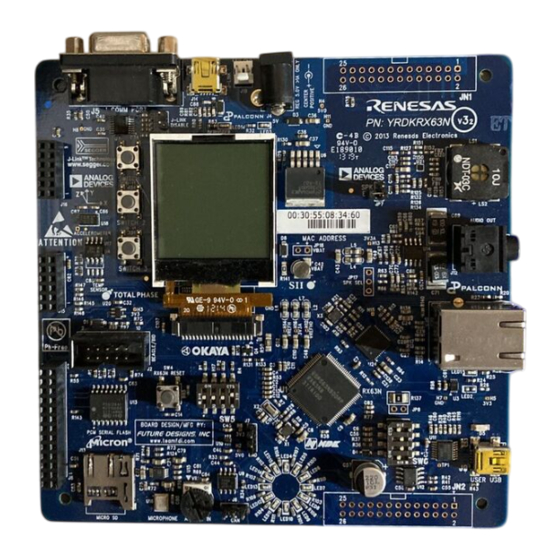
RSK+RX63N-256K 3. Board Layout 3. Board Layout Component Layout Figure 3-1 below shows the top component layout of the board. USB1 USB0 USB0 Ethernet Status LEDs Application Board Interfaces (Function) (Host) (Function) Ethernet Connector RX63N RS232 Serial Application Board Interfaces Debug LCD Header DC Power Jack... -
Page 11: Board Dimensions
RSK+RX63N-256K 3. Board Layout Board Dimensions Figure 3-2 below gives the board dimensions and connector positions. All the through-hole connectors are on a common 0.1 inch grid for easy interfacing. 3.00mm 7.00mm 3.2mm 12.00mm 3.2mm Ether RX63N Battery Holder 7.00mm 8.81mm 10.00mm 19.00mm... -
Page 12: Component Placement
RSK+RX63N-256K 3. Board Layout Component Placement Figure 3-3 below shows placement of individual components on the top-side PCB – bottom-side component placement can be seen in Figure 3-4. Component types and values can be looked up using the board schematics. RCAN R243 SERIAL... - Page 13 RSK+RX63N-256K 3. Board Layout R247 R246 R242 R241 R336 R297 R319 R323 R335 R314 R293 R304 R303 R322 R321 R313 R296 R302 R309 R292 R284 R294 R295 R308 R307 R287 R286 R299 R305 R283 R180 R179 R291 R290 R181 R183 R178 R353 R233...
-
Page 14: Connectivity
RSK+RX63N-256K 4. Connectivity 4. Connectivity Internal RSK+ Connections The diagram below shows the RSK+ board components and their connectivity to the MCU. Power Jack Optional Jacks Backup Battery Boot Mode Switches 128Mbit SDRAM Application Board Headers Mode Pins VBATT 16Kbit I C EEPROM MCU Pin Headers Debug LCD... -
Page 15: Debugger Connections
RSK+RX63N-256K 4. Connectivity Debugger Connections The diagram below shows the connections between the RSK+, E1 debugger and the host PC. External Power LCD Display User Interface Cable USB Cable E1 Emulator CPU Board Host PC Figure 4-2: Debugger Connection Diagram Page 15 of 54 R20UT3076EG0100 Rev. -
Page 16: User Circuitry
RSK+RX63N-256K 5. User Circuitry 5. User Circuitry Reset Circuit A reset control circuit is fitted to the RSK+ to generate the required reset signal, and is triggered from the RES switch. Refer to the RX63N Group, RX631 Group User’s Manual: Hardware for details regarding the reset signal timing requirements, and the RSK+RX63N board schematics for information regarding the reset circuitry in use on the RSK+. -
Page 17: Leds
RSK+RX63N-256K 5. User Circuitry LEDs There are ten LEDs on the RSK+ board. The function of each LED, its colour and connections are shown in Table 5-3. Colour Function MCU Connection 3V3_PWR Green Indicates the status of the 3.3V power rail. No connection 5V_PWR Green... -
Page 18: Rs232 Serial Port
RSK+RX63N-256K 5. User Circuitry RS232 Serial Port Serial port SCI0 is connected to the standard RS232 header fitted to the RSK+. Alternatively, serial port SCI1 or SCI6 can be connected to the RS232 transceiver by making changes to the configurations to the jumpers and option links (refer to §6). -
Page 19: Ethernet
5. User Circuitry Ethernet When running any Ethernet software, a unique MAC address should be used. A unique Renesas allocated MAC address is attached to the RSK+RX63N PCB as a sticker, and should always be used with this device to ensure full compatibility when using other Renesas hardware on a common Ethernet connection. -
Page 20: Universal Serial Bus (Usb)
RSK+RX63N-256K 5. User Circuitry 5.10 Universal Serial Bus (USB) This RSK+ device is fitted with a USB host socket (type A) and a function socket (type Mini B). USB module USB0 is connected to the host and function socket, and can operate as either a host or function device. Module USB1 is connected to a dedicated function port. -
Page 21: Generic Lcd Header
5. User Circuitry 5.11 Generic LCD Header This RSK+ device is fitted with a generic TFT LCD header, that allows connection to compatible Renesas LCD application boards. The pin connections of this header are listed in Table 5-10 below. Generic LCD Header (TFT) -
Page 22: External Bus
Table 5-11: External Bus Address Space 5.13 Renesas Serial Peripheral Interface (RSPI) The RX63N features three Renesas Serial Peripheral Interface modules (Renesas SPI or RSPI). Table 5-12 below details the connected devices, and their connections to the MCU. RSPI Channel... -
Page 23: Configuration
RSK+RX63N-256K 6. Configuration 6. Configuration Modifying the RSK+ This section lists the option links that are used to modify the way RSK+ operates in order to access different configurations. Configurations are made by modifying link resistors or headers with movable jumpers or by configuration DIP switches A link resistor is a 0Ω... -
Page 24: Adc Configuration
RSK+RX63N-256K 6. Configuration Table 6-3 below details the different configurations and functions of the MCU operating mode jumpers. Reference Position One Position Two Position Three Related Ref. Pins 1 and 2 shorted. Pins 2 and 3 shorted. All pins open. EMLE is left Connects EMLE (U1B, Connects EMLE (U1B, to float –... -
Page 25: Rs232 Serial Port Configuration
RSK+RX63N-256K 6. Configuration Reference Link Fitted Configuration Link Removed Configuration Related Ref. R87* Connects AN005_YINPUT1 (U1C, pin Disconnects AN005_YINPUT1 167) to AN005 (JA5, pin 2). (U1C, pin 167) from AN005 (JA5, pin 2). R89* Connects AN006_XINPUT2 (U1C, pin Disconnects AN006_XINPUT2 166) to AN006 (JA5, pin 3). -
Page 26: Can Configuration
RSK+RX63N-256K 6. Configuration Table 6-7 below details the different configurations and functions of the RS232 serial jumpers. Reference Position One Position Two Position Three Related Ref. (Pin 1 and 2 Shorted) (Pin 2 and 3 Shorted) (All Pins Open) Disconnects both lines. Connects TXD0 (U1B, Connects TXD1 (U1B, R59, R60*... -
Page 27: External Bus Configuration
RSK+RX63N-256K 6. Configuration Table 6-9 below details the different configurations and functions of the CAN jumpers. Reference Position One Position Two Position Three Related Ref. (Pin 1 and 2 Shorted) (Pin 2 and 3 Shorted) (All Pins Open) J14* Connects VBAT (U11, Connects VBAT (U11, VBAT (U11, pin 10) is not R245... - Page 28 RSK+RX63N-256K 6. Configuration Reference Link Fitted Configuration Link Removed Configuration Related Ref. R230* Connects BCLK (U1C, pin 68) to Disconnects BCLK (U1C, pin 68) R229* JA3_PIN44 (JA3, pin 44). from JA3_PIN44 (JA3, pin 44). R232* Connects WAITn (U1C, pin 66) to Disconnects WAITn (U1C, pin 66) R100*, R231 JA3_PIN45 (JA3, pin 45).
-
Page 29: Usb Configuration
RSK+RX63N-256K 6. Configuration USB Configuration Table 6-12 & Table 6-13 below details the function of option links related to configuring the USB ports. Reference Link Fitted Configuration Link Removed Configuration Related Ref. Connects MTCLKB_USB1DPUPE Disconnects MTCLKB_USB1DPUPE R54* (U1B, pin 50) to USB1DPUPE. (U1B, pin 50) from USB1DPUPE. - Page 30 RSK+RX63N-256K 6. Configuration Reference Link Fitted Configuration Link Removed Configuration Related Ref. R280 Connects FRAME (USB Connectors: Disconnects FRAME (USB Connectors: USB_1 Function) to GROUND. USB_1 Function) from GROUND. R281* Connects VBUS0 to VBUS Disconnects VBUS0 from VBUS. J20* R373 Connects USB0DP (U1B, pin 59) to D+ Disconnects USB0DP (U1B, pin 59) from (USB Connectors: USB0_2 and...
- Page 31 RSK+RX63N-256K 6. Configuration Table 6-17 below details the different configurations and functions of the USB jumpers. Reference J17* J20* Function Position Pin 1 and 2 shorted Pin 1 and 2 shorted Bus-powered (via R281) Pin 2 and 3 shorted All open Self-powered (via R265) Table 6-17: USB Jumpers (VBUS0 Self-powered/Bus-powered Configuration)
-
Page 32: Ethernet Configuration
RSK+RX63N-256K 6. Configuration Ethernet Configuration Table 6-21 & Table 6-22 below details the function of option links related to configuring the MCU’s Ethernet peripheral. Reference Link Fitted Configuration Link Removed Configuration Related Ref. R98* Connects CTX1_ALE_ETLINKSTA to Disconnects R96, R97* ETLINKSTA (U14, pin 10). - Page 33 RSK+RX63N-256K 6. Configuration Reference Link Fitted Configuration Link Removed Configuration Related Ref. Disconnects XTAL2 (U14, pin 13) from R325 Connects XTAL2 (U14, pin 13) to X4 X4 (pin 2). (pin 2). Connects XTAL1 (U14, pin 14) to X5 (pin R326* Disconnects XTAL1 (U14, pin 14) R327*, R324 from X5 (pin 3).
-
Page 34: Multi-Function Timer Pulse Unit (Mtu) Configuration
RSK+RX63N-256K 6. Configuration Multi-Function Timer Pulse Unit (MTU) Configuration Table 6-23 & Table 6-24 details the function of option links related to configuring the MCU’s MTU pins. Reference Link Fitted Configuration Link Removed Configuration Related Ref. R45* Connects LED2_MTIC5W (U1B, pin 56) Disconnects LED2_MTIC5W (U1B, pin to MTIC5W (JA6, pin 16). -
Page 35: Irq & General I/O Pin Configuration
RSK+RX63N-256K 6. Configuration Reference Link Fitted Configuration Link Removed Configuration Related Ref. R106* Connects ETRXDV_MTIOC4B (U1C, pin Disconnects ETRXDV_MTIOC4B (U1C, R105 86) to MTIOC4B (JA2, pin 17) via U15. pin 86) from MTIOC4B (JA2, pin 17). R108* Connects ETTXER_MTIOC4D (U1C, pin Disconnects ETTXER_MTIOC4D (U1C, R107 83) to MTIOC4D (JA2, pin 18) via U15. - Page 36 RSK+RX63N-256K 6. Configuration Reference Link Fitted Configuration Link Removed Configuration Related Ref. Connects LED0_DA0 (U1B, pin 4) to Disconnects LED0_DA0 (U1B, pin 4) R41* LED0 from LED0 Connects LED1_DA1 (U1B, pin 2) to Disconnects LED1_DA1 (U1B, pin 2) R43* LED1 from LED1 Connects LED2_MTIC5W (U1B, pin Disconnects LED2_MTIC5W (U1B,...
-
Page 37: Power Supply Configuration
RSK+RX63N-256K 6. Configuration Table 6-27 below details the function of the jumpers associated with IRQ and general I/O pin configuration. Reference Position One Position Two Position Three Related Ref. Pins 1 and 2 Pins 2 and 3 shorted. All pins open. shorted. - Page 38 RSK+RX63N-256K 6. Configuration Reference Link Fitted Configuration Link Removed Configuration Related Ref. R153* CON_3V3USB is supplied power from CON_3V3USB is not supplied R154 Board_VCC. power from Board_VCC. R154 Enables Board_VCC to supply power Disables Board_VCC from supplying R150 to CON_3V3USB and 3V3USB. power to CON_3V3USB and 3V3USB.
-
Page 39: Clock Configuration
RSK+RX63N-256K 6. Configuration 6.12 Clock Configuration Table 6-32 below details the function of the option links associated with clock configuration. Reference Link Fitted Configuration Link Removed Configuration Related Ref. R17* X1 feedback resistor. Connects X1 pins X1 feedback resistor. Connects X1 1 and 2. - Page 40 RSK+RX63N-256K 6. Configuration Table 6-34 below details the function of the jumper associated with external memory configuration. Reference Position One Position Two Position Three Related Ref. Pins 1 and 2 shorted. All pins open. WP (U5, pin R137* Connects WP (U5, pin 7) 7) is disconnected from to GROUND, disabling GROUND, enabling write...
-
Page 41: Headers
7. Headers 7. Headers Application Headers This RSK+ is fitted with application headers, which can be used to connect compatible Renesas application devices or as easy access to MCU pins. Table 7-1 below lists the connections of the application header, JA1. - Page 42 RSK+RX63N-256K 7. Headers Table 7-2 below lists the connections of the application header, JA2. Application Header JA2 Function (Header Name) Function (Header Name) MCU Pin MCU Pin Circuit Net Name Circuit Net Name RESET EXTAL RESn CON_EXTAL Vss1 NMIn GROUND WDT_OVF SCIaTX TXD0...
- Page 43 RSK+RX63N-256K 7. Headers Table 7-3 below lists the connections of the BUS application header, JA3 Bus Application Header JA3 Function (Header Name) Function (Header Name) MCU Pin MCU Pin Circuit Net Name Circuit Net Name D0_IO0 D1_IO1 D2_IO2 D3_IO3 D4_IO4 D5_IO5 D6_IO6 D7_IO7...
- Page 44 RSK+RX63N-256K 7. Headers Table 7-4 below lists the connections of the application header, JA5. Application Header JA5 Function (Header Name) Function (Header Name) MCU Pin MCU Pin Circuit Net Name Circuit Net Name ADC4 ADC5 AN004 AN005 ADC6 ADC7 AN006 AN007 CAN1TX CAN1RX...
- Page 45 RSK+RX63N-256K 7. Headers Table 7-5 below lists the connections of the application header, JA6. Application Header JA6 Function (Header Name) Function (Header Name) MCU Pin MCU Pin Circuit Net Name Circuit Net Name DREQ DACK EDREQ1 EDACK1 TEND STBYn RS232TX RS232RX RS232TX RS232RX...
-
Page 46: Generic Headers
RSK+RX63N-256K 7. Headers Generic Headers Generic headers, used to provide easy connections to various pins from devices fitted to the RSK+. Table 7-6 below lists the connections of the Data Bus Connector, J22. 32bit Data Bus Connector J22 Function (Header Name) Function (Header Name) MCU Pin MCU Pin... - Page 47 RSK+RX63N-256K 7. Headers Table 7-7 below lists the connections of the Generic LCD Header (TFT). Generic LCD Header (TFT) Function (Header Name) Function (Header Name) MCU Pin MCU Pin Circuit Net Name Circuit Net Name Board_5V Board_5V Board_VCC Board_VCC Reserved Reserved D0_IO0 D1_IO1...
-
Page 48: Code Development
8. Code Development Overview For all code debugging using Renesas software tools, the RSK+ board must be connected to a PC via an E1/E20 debugger. An E1 debugger is supplied with this RSK+ product. For further information regarding the debugging capabilities of the E1/E20 debuggers, refer to the RX Family E1/E20 Emulator User’s Manual (R20UT0398EJ). -
Page 49: Address Space
RSK+RX63N-256K 8. Code Development Address Space Figure 8-1 below details the address space of MCU in its different operating modes. For further details, refer to the RX63N Group, RX631 Group User's Manual: Hardware. Figure 8-1: MCU Address Space Diagram Page 49 of 54 R20UT3076EG0100 Rev. -
Page 50: Additional Information
Copyright This document may be, wholly or partially, subject to change without notice. All rights reserved. Duplication of this document, either in whole or part is prohibited without the written permission of Renesas Electronics Europe Limited. © 2014 Renesas Electronics Europe Limited. All rights reserved. - Page 51 REVISION HISTORY RSK+RX63N-256K User’s Manual (for e studio) Rev. Date Description Page Summary 1.00 Aug 14, 2014 First Edition issued...
- Page 52 Renesas Starter Kit+ User’s Manual: User’s Manual Publication Date Rev.1.00 Aug, 2014 Published by: Renesas Electronics Corporation...
- Page 53 SALES OFFICES http://www.renesas.com Refer to "http://www.renesas.com/" for the latest and detailed information. Renesas Electronics America Inc. 2801 Scott Boulevard Santa Clara, CA 95050-2549, U.S.A. Tel: +1-408-588-6000, Fax: +1-408-588-6130 Renesas Electronics Canada Limited 1101 Nicholson Road, Newmarket, Ontario L3Y 9C3, Canada...
- Page 54 RX63N Group R20UT3076EG0100 Rev. 1.00...
- Page 55 Mouser Electronics Authorized Distributor Click to View Pricing, Inventory, Delivery & Lifecycle Information: Renesas Electronics YR0K50563NS010BE...
Need help?
Do you have a question about the RX63N Series and is the answer not in the manual?
Questions and answers