Advertisement
Quick Links
CONTENTS
1
INTRODUCTION ....................................................................................................... 1
2
SETUP ....................................................................................................................... 3
3
BILL OF MATERIALS .............................................................................................. 6
4
SCHEMATIC ............................................................................................................. 7
1
DS100MB203EVK (TOP / BOTTOM VIEW) .............................................................. 1
2
DS100MB203EVK Schematic ................................................................................... 7
1
Switches to set the 4-level input control pins ............................................................. 2
2
Connection and Control Description ......................................................................... 2
3
16 EQ settings when in pin mode .............................................................................. 4
4
16 settings of VOD and DE when in pin mode .......................................................... 4
1. Introduction:
The DS100MB203EVK is a dual Lane 2:1/1:2 Mux/Buffer SMA evaluation kit. It provides a complete high
bandwidth platform to evaluate the signal integrity and signal conditioning features of the DS100MB203SQ -
10.3125 Gbps Dual Lane 2:1/1:2 Mux/Buffer with Equalization and De-Emphasis.
October 2012
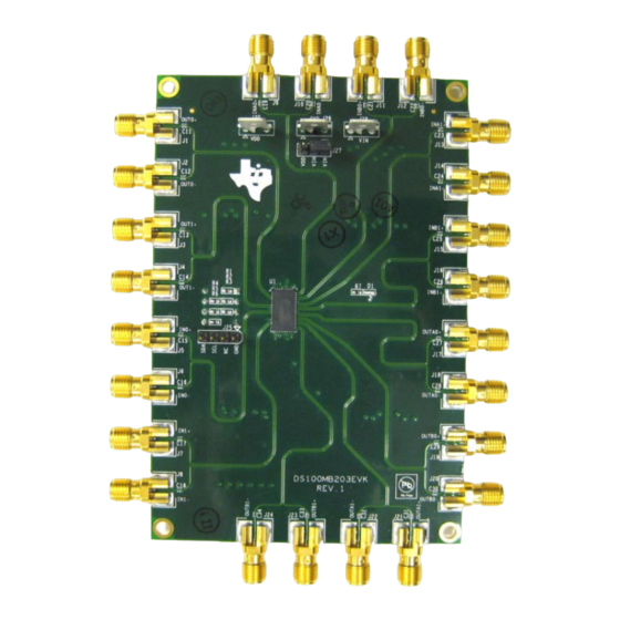
Figure 1. DS100MB203EVK (TOP / BOTTOM VIEW)
DS100MB203EVK User's Guide
LIST OF FIGURES
LIST OF TABLES
DS100MB203EVK User's Guide
User's Guide
October 2012
1
Advertisement

Related Manuals for Texas Instruments DS100MB203EVK


Summary of Contents for Texas Instruments DS100MB203EVK
-
Page 1: Table Of Contents
16 settings of VOD and DE when in pin mode ............4 1. Introduction: The DS100MB203EVK is a dual Lane 2:1/1:2 Mux/Buffer SMA evaluation kit. It provides a complete high bandwidth platform to evaluate the signal integrity and signal conditioning features of the DS100MB203SQ –... -
Page 2: Switches To Set The 4-Level Input Control Pins
VDD_SEL – Enable or disable the internal 3.3V to 2.5V regulator (GND – enables the internal LDO for 3.3V to 2.5V). RESET RESET – Enable or disable the device (GND – enables the device). EQ_D[1:0] PIN MODE – EQ control for channel D inputs DS100MB203EVK User’s Guide October 2012... -
Page 3: Setup
INPUT_EN pin 0: Normal Operation, FANOUT is disabled, use SEL0/1 to select the A or B input/output (see SEL0/1 pin), input always enabled with 50 ohms. INPUT_EN R: Reserved (DO NOT USE). F: AUTO - Use RX Detect, SEL0/1 to determine which input or output to enable, FANOUT is disable 1: Normal Operation, FANOUT is enabled (both S_OUT0/1 are ON). - Page 4 0, R 0, F -3.5 0, 1 R, 0 -3.5 R, R R, F R ,1 -3.5 F ,0 F, R F, F -3.5 F, 1 1, 0 1, R -3.5 1, F 1, 1 DS100MB203EVK User’s Guide October 2012...
- Page 5 2.7. For SMBUS mode control of the EQ, VOD and De-emphasis level: Set ENSMB = 1 (1kohm to VIH) by using the SW2 (3-2-1) = (OFF-OFF-ON). Set SW4 pin1,2 to the ON position so the SMBUS signals are connected. Set SW3 pin1 thru pin6 switches to the OFF position so they do not connect to the SDA and SCL line. Set the SW1 and SW5 for the AD[3:0] pins.
-
Page 6: Bill Of Materials
4. Bill of Materials for DS100MB203EVK: Item Reference Digikey PN Manufacture PN Descriptions 445-3448-1-ND C1608Y5V0J106Z CAP CER 10UF 6.3V Y5V 0603 445-1322-1-ND C1608X5R0J105K CAP CER 1.0UF 6.3V X5R 10% 0603 C3,C4,C5,C6,C7,C8 445-4711-1-ND C0603X5R0J104M CAP CER .10UF 6.3V X5R 0201 C11,C12,C13,C14,C15,C16... -
Page 7: Schematic
5. Schematic Figure 2. DS100MB203EVK Schematic October 2012 SNLU120... - Page 8 EVALUATION BOARD/KIT/MODULE (EVM) ADDITIONAL TERMS Texas Instruments (TI) provides the enclosed Evaluation Board/Kit/Module (EVM) under the following conditions: The user assumes all responsibility and liability for proper and safe handling of the goods. Further, the user indemnifies TI from all claims arising from the handling or use of the goods.
- Page 9 This equipment has been tested and found to comply with the limits for a Class A digital device, pursuant to part 15 of the FCC Rules. These limits are designed to provide reasonable protection against harmful interference when the equipment is operated in a commercial environment. This equipment generates, uses, and can radiate radio frequency energy and, if not installed and used in accordance with the instruction manual, may cause harmful interference to radio communications.
- Page 10 Please note that if you could not follow the instructions above, you will be subject to penalties of Radio Law of Japan. Texas Instruments Japan Limited (address) 24-1, Nishi-Shinjuku 6 chome, Shinjuku-ku, Tokyo, Japan http://www.tij.co.jp...
- Page 11 FDA Class III or similar classification, then you must specifically notify TI of such intent and enter into a separate Assurance and Indemnity Agreement. Mailing Address: Texas Instruments, Post Office Box 655303, Dallas, Texas 75265 Copyright © 2012, Texas Instruments Incorporated...
- Page 12 IMPORTANT NOTICE Texas Instruments Incorporated and its subsidiaries (TI) reserve the right to make corrections, enhancements, improvements and other changes to its semiconductor products and services per JESD46, latest issue, and to discontinue any product or service per JESD48, latest issue.
-
Page 13: Ds100Mb203Evk (Top / Bottom View)
Mouser Electronics Authorized Distributor Click to View Pricing, Inventory, Delivery & Lifecycle Information: Texas Instruments DS100MB203EVK/NOPB...
Need help?
Do you have a question about the DS100MB203EVK and is the answer not in the manual?
Questions and answers