Table of Contents
Advertisement
Quick Links
www.ti.com
User's Guide
TLV841EVM Voltage Supervisor User Guide
Ben Chan
This user guide describes the TLV841EVM evaluation module (EVM). This guide contains the EVM schematic,
bill of materials (BOM), assembly drawing, and top and bottom board layouts.
1
Introduction.............................................................................................................................................................................2
Documentation......................................................................................................................................................3
Applications...........................................................................................................................................................3
2 Schematic, Bill of Materials, and Layout..............................................................................................................................
2.1 TLV841EVM Schematic.....................................................................................................................................................
Materials..............................................................................................................................................6
2.4 Layout................................................................................................................................................................................
3 EVM Connectors.....................................................................................................................................................................
Points.................................................................................................................................................................9
Jumpers...................................................................................................................................................................10
4 EVM Setup and Operation....................................................................................................................................................
).............................................................................................................................................................11
4.2 Monitoring Voltage on SENSE Pin (TLV841S).................................................................................................................
4.3 Monitoring Voltage on VDD (TLV841M and TLV841C)....................................................................................................
4.4 Manual Reset (MR) (TLV841M).......................................................................................................................................
(RESET).....................................................................................................................................................12
5 Revision History...................................................................................................................................................................
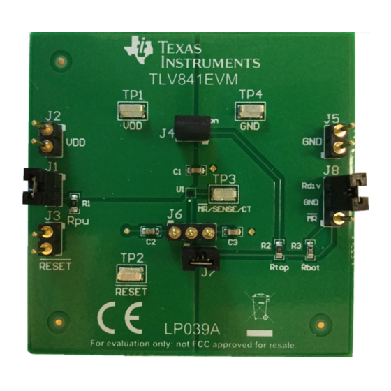
Figure 1-1. TLV841EVM Board Top.............................................................................................................................................
Figure 1-2. TLV841EVM Board Bottom.......................................................................................................................................
Figure 2-1. TLV841EVM Schematic with TLV841S.....................................................................................................................
Figure 2-3. Component Placement-Bottom Assembly..............................................................................................................
Figure 2-4. Layout-Top..............................................................................................................................................................
Layout-Bottom.........................................................................................................................................................7
Layer...................................................................................................................................................................8
Figure 2-7. Bottom Layer.............................................................................................................................................................
Mask........................................................................................................................................................8
Figure 4-2. TLV841EVM RESET Propagation Detect Delay.....................................................................................................
BOM............................................................................................................................................................................6
Table 3-1. Test Points..................................................................................................................................................................
Jumpers...........................................................................................................................................10
Table 4-1. Nominal Input Threshold Voltage..............................................................................................................................
Trademarks
All trademarks are the property of their respective owners.
SNVU755A - JANUARY 2021 - REVISED JUNE 2021
Submit Document Feedback
ABSTRACT
Table of Contents
Placement....................................................................................................................................7
)
D
T
List of Figures
Assembly....................................................................................................................7
Immunity...................................................................................................................................12
List of Tables
Copyright © 2021 Texas Instruments Incorporated
(TLV841C)....................................................................................13
TLV841EVM Voltage Supervisor User Guide
Table of Contents
...........................14
4
5
7
9
11
11
12
12
14
2
3
5
7
7
8
13
9
11
1
Advertisement
Table of Contents

Related Manuals for Texas Instruments TLV841EVM


Summary of Contents for Texas Instruments TLV841EVM
-
Page 1: Table Of Contents
User’s Guide TLV841EVM Voltage Supervisor User Guide Ben Chan ABSTRACT This user guide describes the TLV841EVM evaluation module (EVM). This guide contains the EVM schematic, bill of materials (BOM), assembly drawing, and top and bottom board layouts. Table of Contents Introduction.....................................2 1.1 Related... -
Page 2: Introduction
The TLV841EVM also can accommodate push-pull variants (TLV841xxPLxx or TLV841xxPHxx). If a push-pull variant is placed onto the TLV841EVM, the shunt on J1 must be removed as push-pull devices do not use a pull-up resistor. Therefore, R1 on the TLV841EVM must be disconnected. Please also note if using TLV841EVM with the active-high variant (TLV841xxPHxx), the active-low RESET label on the EVM board and throughout this User Guide becomes active-high RESET. -
Page 3: Related Documentation
Introduction Figure 1-2. TLV841EVM Board Bottom 1.1 Related Documentation TLV841 Tiny Nano-Power, Ultra-Low Voltage Supervisor in WCSP Package data sheet, TLV841. 1.2 TLV841 Applications • Personal electronics • Home theater and entertainment • Electronic point of sale • Grid infrastructure •... -
Page 4: Schematic, Bill Of Materials, And Layout
Schematic, Bill of Materials, and Layout www.ti.com 2 Schematic, Bill of Materials, and Layout This section provides a detailed description of the TLV841EVM schematic, bill of materials (BOM), and layout. TLV841EVM Voltage Supervisor User Guide SNVU755A – JANUARY 2021 – REVISED JUNE 2021 Submit Document Feedback Copyright ©... -
Page 5: Tlv841Evm Schematic
Schematic, Bill of Materials, and Layout 2.1 TLV841EVM Schematic Figure 2-1. TLV841EVM Schematic with TLV841S SNVU755A – JANUARY 2021 – REVISED JUNE 2021 TLV841EVM Voltage Supervisor User Guide Submit Document Feedback Copyright © 2021 Texas Instruments Incorporated... -
Page 6: Tlv841Evm Bill Of Materials
Schematic, Bill of Materials, and Layout www.ti.com 2.2 TLV841EVM Bill of Materials Table 2-1. BOM PACKAGE DESIGNATOR VALUE DESCRIPTION PART NUMBER MANUFACTURER REFERENCE Printed Circuit Board TLV841EVM C1, C3 0.1 µF CAP, CERM, 0.1 µF, 0603 C0603C104K4RACTU Kemet 16 V, ± 10%, X7R, 0603 0.01 µF... -
Page 7: Layout And Component Placement
2.4 Layout Figure 2-2. Component Placement—Top Assembly Figure 2-3. Component Placement—Bottom Assembly Figure 2-5. Layout—Bottom Figure 2-4. Layout—Top SNVU755A – JANUARY 2021 – REVISED JUNE 2021 TLV841EVM Voltage Supervisor User Guide Submit Document Feedback Copyright © 2021 Texas Instruments Incorporated... -
Page 8: Figure 2-6. Top Layer
Schematic, Bill of Materials, and Layout www.ti.com Figure 2-6. Top Layer Figure 2-7. Bottom Layer Figure 2-8. Top Solder Mask TLV841EVM Voltage Supervisor User Guide SNVU755A – JANUARY 2021 – REVISED JUNE 2021 Submit Document Feedback Copyright © 2021 Texas Instruments Incorporated... -
Page 9: Evm Connectors
RESET output. Connection to GND pin. Allows the user to connect to the ground plane. SNVU755A – JANUARY 2021 – REVISED JUNE 2021 TLV841EVM Voltage Supervisor User Guide Submit Document Feedback Copyright © 2021 Texas Instruments Incorporated... -
Page 10: Evm Jumpers
EVM Connectors www.ti.com 3.2 EVM Jumpers Table 3-2 lists the jumpers on the TLV841EVM. As ordered, the EVM will have eight (8) jumpers and five (5) shunts installed. Table 3-2. List of Onboard Jumpers JUMPER JUMPER CONFIGUATION DESCRIPTION Connect a shunt to jumper J1 to use R1 as the pull-up resistor on the output RESET Shunted pin. -
Page 11: Evm Setup And Operation
EVM Setup and Operation 4 EVM Setup and Operation This section describes the functionality and operation of the TLV841EVM. The user must read the TLV841 datasheet for electrical characteristics of the device. 4.1 Input Power (V The VDD supply is connected through the J2 header on board. Both pins of jumper J2 are connected together where power can be applied to either pin. -
Page 12: Monitoring Voltage On Vdd (Tlv841M And Tlv841C)
J1 open and connecting the pull-up voltage to pin 2 [V ] of jumper J1. The TLV841EVM provides jumper J3 and test point TP2 that is connected directly to the RESET pin for monitoring and/or interfacing to other devices. -
Page 13: Reset Time Delay Programming (Program T Via C (Tlv841C)
) = 26.4 ¡ ¢ P_HL Figure 4-2. TLV841EVM RESET Propagation Detect Delay 4.6 Reset Time Delay Programming (Program t via C ) (TLV841C) The TLV841C device variant has two options for setting the RESET time delay: connect CT pin to a capacitor to GND, or leave CT pin floating. -
Page 14: Revision History
The TLV841EVM provides jumper J6 to configure the CT pin and test point TP3 to monitor the CT pin. Place a shunt jumper on pin 1 (left pin) and pin 2 (middle pin) of jumper J6 to connect CT to delay capacitor C2. This connects the CT pin to a 0.01 µF capacitor to set the RESET delay (t... - Page 15 STANDARD TERMS FOR EVALUATION MODULES Delivery: TI delivers TI evaluation boards, kits, or modules, including any accompanying demonstration software, components, and/or documentation which may be provided together or separately (collectively, an “EVM” or “EVMs”) to the User (“User”) in accordance with the terms set forth herein.
- Page 16 www.ti.com Regulatory Notices: 3.1 United States 3.1.1 Notice applicable to EVMs not FCC-Approved: FCC NOTICE: This kit is designed to allow product developers to evaluate electronic components, circuitry, or software associated with the kit to determine whether to incorporate such items in a finished product and software developers to write software applications for use with the end product.
- Page 17 www.ti.com Concernant les EVMs avec antennes détachables Conformément à la réglementation d'Industrie Canada, le présent émetteur radio peut fonctionner avec une antenne d'un type et d'un gain maximal (ou inférieur) approuvé pour l'émetteur par Industrie Canada. Dans le but de réduire les risques de brouillage radioélectrique à...
- Page 18 www.ti.com EVM Use Restrictions and Warnings: 4.1 EVMS ARE NOT FOR USE IN FUNCTIONAL SAFETY AND/OR SAFETY CRITICAL EVALUATIONS, INCLUDING BUT NOT LIMITED TO EVALUATIONS OF LIFE SUPPORT APPLICATIONS. 4.2 User must read and apply the user guide and other available documentation provided by TI regarding the EVM prior to handling or using the EVM, including without limitation any warning or restriction notices.
- Page 19 Notwithstanding the foregoing, any judgment may be enforced in any United States or foreign court, and TI may seek injunctive relief in any United States or foreign court. Mailing Address: Texas Instruments, Post Office Box 655303, Dallas, Texas 75265 Copyright © 2019, Texas Instruments Incorporated...
- Page 20 TI products. TI’s provision of these resources does not expand or otherwise alter TI’s applicable warranties or warranty disclaimers for TI products.IMPORTANT NOTICE Mailing Address: Texas Instruments, Post Office Box 655303, Dallas, Texas 75265 Copyright © 2021, Texas Instruments Incorporated...
Need help?
Do you have a question about the TLV841EVM and is the answer not in the manual?
Questions and answers