Table of Contents
Advertisement
Quick Links
ORDER NO. KMS0308816C1
F19
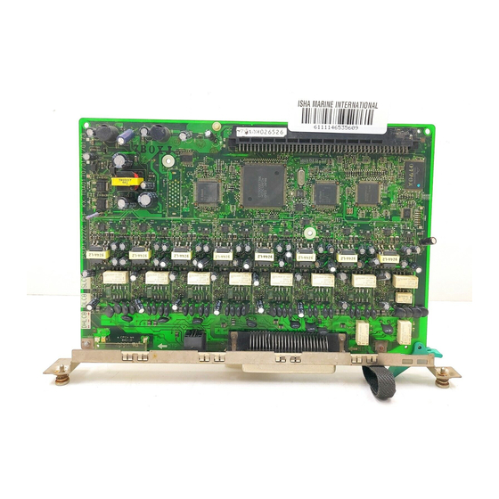
8Port Digital Hybrid Extension Card
KX-TDA0170
(for U.S.A.)
2003 Panasonic Communications Co., Ltd. All rights reserved.
Unauthorized copying and distribution is a violation of law.
IMPORTANT INFORMATION ABOUT LEAD FREE, (PbF), SOLDERING
If lead free solder was used in the manufacture of this product the printed circuit boards will be
marked PbF.
Standard leaded, (Pb), solder can be used as usual on boards without the PbF mark.
When this mark does appear please read and follow the special instructions described in this
manual on the use of PbF and how it might be permissible to use Pb solder during service and
repair work.
1. ABOUT LEAD FREE SOLDER (PbF: Pb free)
Note:
In the information below, Pb, the symbol for lead in the periodic table of elements, will refer to
1
Advertisement
Table of Contents

Related Manuals for Panasonic KX-TDA0170


Summary of Contents for Panasonic KX-TDA0170
- Page 1 8Port Digital Hybrid Extension Card KX-TDA0170 (for U.S.A.) 2003 Panasonic Communications Co., Ltd. All rights reserved. Unauthorized copying and distribution is a violation of law. IMPORTANT INFORMATION ABOUT LEAD FREE, (PbF), SOLDERING If lead free solder was used in the manufacture of this product the printed circuit boards will be marked PbF.
- Page 2 standard solder or solder that contains lead. We will use PbF solder when discussing the lead free solder used in our manufacturing process which is made from Tin, (Sn), Silver, (Ag), and Copper, (Cu). This model, and others like it, manufactured using lead free solder will have PbF stamped on the PCB.
- Page 3 1.2. HOW TO RECOGNIZE THAT Pb FREE SOLDER IS USED “PbF” is marked on the PCB to show that Pb free solder is used.(See the figure below.)
-
Page 4: For Service Technicians
2. FOR SERVICE TECHNICIANS ICs and LSIs are vulnerable to static electricity. When repairing, the following precautions will help prevent recurring malfunctions. -
Page 5: General Description
1. Cover the plastic parts boxes with aluminum foil. 2. Ground the soldering irons. 3. Use a conductive mat on the worktable. 4. Do not touch IC or LSI pins with bare fingers. 3. GENERAL DESCRIPTION This card, which is used in the free slot of the TDA system, can randomly connect eight of SLT, DPT, and APT. -
Page 6: Names And Locations
Functional Block Functional contents DTMF Receiver Eight lines for each port On-board Ringer 20/25Hz 75Vrms Phase control (Three-phase / Four-phase) On-board DC/DC Power Input +15V Supply Output +15V, +5V, +3.3V Power Failure Forwarding Two lines supported Function Self-Diagnostic Function Carried out with outsire-line interface in a pair (DHLC8 card has only Speech path test, Dial pulse test, DTMF test ASIC EC bus interface function... - Page 7 Note: *Null slot is not available for any optional service cards. 5.1. INSTALLING/REMOVING THE OPTIONAL SERVICE CARDS Slot Condition Card Type Slot Type Option Slot MPR Slot KX-TDA100: Free Slots 1 to 5 KX-TDA200: Free Slots 1 to 10 MPR Card CO Line Cards Extension Cards OPB3 Card...
- Page 8 Notes - To connect the amphenol connector, refer to "Fastening Amphenol Type Connector". - For details about power failure transfer, refer to "Auxiary Connection for Power Failure Transfer". Accessory and User-supplied ltems Accessory: screws x 2 User-supplied: amphenol connector Pin Assignments Amphenol Connector...
- Page 9 Signal Name Function Signal Name Function SLT Ring port 1 SLT Tip port 1 PT Data port 1 (Low PT Data port 1 (High Volt) Volt) Reserved Reserved SLT Ring port 2 SLT Tip port 2 PT Data port 2 (Low PT Data port 2 (High Volt) Volt)
- Page 10 Indication Color Description CARD Green/Red OFF: Power Off STATUS Green ON: Normal (all ports are idle) Green Flash (60 times per minute ): Normal (a port is in use) Red ON: Fault (includes reset) Red Flash (60 times per minute): Out of Service Fastening Amphenol Type Connector An amphenol 57JE type connector is used on some of the optional sevice cards.
- Page 11 DHLC8 (2 PFT port) and SLC8 (2 PFT port) Note Pin assignments for ports 3 and 4 are the same as those of ports 1 and 2. Accessory and User-supplied ltems Accessory: none User-supplied: RJ11 connectors RJ11 Connector Pin Assignments for CO line Crad No.
- Page 12 1. Insert the card along the guide rails. 2. Holding the card as follows, push the release lever in the direction of the arrow so that the card is made to engage with the connector on the back board securely. 3.
-
Page 13: Troubleshooting Guide
6. TROUBLESHOOTING GUIDE... -
Page 21: Block Diagram
7. BLOCK DIAGRAM... -
Page 22: Circuit Operation
8. CIRCUIT OPERATION 8.1. Control-System Circuit 8.1.1. CPU Peripherals - CPU (System clock: 12.288 MHz)..IC507 Data bus: 16bit, Address bus: 23bit - Flash ROM (8Mbit)..IC504 Flash memory consists of two areas: boot space and administration space. administration program can be rewritten through downloading. - SRAM (2Mbit)..IC503, IC506 Used for the data buffer for CPU work area, and PT communication. - Page 23 recovered from by the edge detection of nIRQ0 - LED Operation status indicating LED (Two colors) Red ON: Fault (RESET included) Green ON: INS (Line not in use) Green Flash (60/minute): INS (Line in use) Red blinking: OUS OFF: Power supply failure - Address map 8.1.2.
- Page 24 - Local bus interface HITACHI-manufactured (Data 8bit, Address 13bit) SH-1CPU- compatible bus. - Local highway interface Accommodates 2.048, 4.096, and 8.192MHz highways (Up to 64 time slots). - Local TSW Exchanges the time slots between CT bus (1024ch) and local highway (64ch).
- Page 25 - APT data communications Control data is transmitted from the DTL terminal of ASIC, then is output to APT (between D1 and D2) by way of the driver U5 and the pulse transformer T1. The control data transmitted from APT is input to the DR terminal of ASIC by way of the pulse transformer T1 and R13.
- Page 26 Used mainly for the control signal of DPT. - Cch communications Communicated by the data (8kbps) converted by the serial/parallel- converting circuit in ASIC. Used mainly for recognizing the terminal model. - PT current-supply circuit +15V/+40V is superimposed on the transmit/receive data line (D1, D2), and fed to PT.
- Page 27 detection, BELL relay control, and DIAG relay control. - A/D, D/A conversion The conversion of 4-line analog signal and G.711 format PCM code ( /A) is carried out. - SLT current-supply circuit The current-supply circuit feeds current at the constant-current circuit (TIP +30V, RING 0V).
- Page 28 the front of the board and 4-conductor TEL cord. In normal operation, the switching relays are in ‘make’ state. In case of power supply down, they will be in ‘break’ state, and the power- failure direct-dial mode will be established. - Self-diagnostic relay A port has a self-diagnostic relay.
- Page 29 While BELL signal is issued, when SLT is on hook, U52 (1, 2, and 6 pin) is off. When SLT is taken off the hook, DC loop is formed because 30V is superimposed on BELL signal; then, current flows into R52 U52, and U52 (1, 2, and 6 pin) becomes When U52 (1, 2, and 6 pin) has become on, because the base of Q57 that is the driver of BELL relay becomes L, BELL relay will be...
- Page 30 This circuit generates +3.3V, +5V from the input +15V. It is comprised of the circuit that steps +15V down to +3.3V by the switching power supply of IC801, Q801, and L810 and the one that steps +15V down to +5V by the switching power supply of IC802, Q802, and L811.
- Page 31 8.3.3. Power Supply System Power-supply input includes four systems: +15V, +15VPT, +40V, and +30V; the output includes + 15V, +5V, +3.3V, +40V. 9. IC DATA 9.1. IC7 (ASIC)
- Page 32 Pin No. Signal name Description Remarks name VER5 RAM (H: 2Mbit, L: 1Mbit) VER4 Card distinguishing reserve VER3 VER2 For hard version management VER1 For the first time, 0 VER0 PORT1 Number of ports: 8 PORT0 DTH7 Port 7 PT transmit pulse Used DTH6 Port 6 PT transmit pulse...
- Page 33 Pin No. Signal name Description Remarks name LED_G Green LED lit / CS_DELAY output LED_R Red LED lit BELL CNT Bell circuit stop OPTION 0 Option board 0 detection DTL7 Port 7 PT transmit pulse Used DTL6 Port 6 PT transmit pulse Used DTL5 Port 5 PT transmit pulse...
- Page 34 Pin No. Signal name Description Remarks name PA15 FH Frame head detection Used nIRQ3 PA14 BELL_SYNC BELL phase detection Used nIRQ2 PA13 nIRQ1 MPR interrupt Used nIRQ1 PA12 HALT DC power down recovery detection Used nIRQ0 PA11 nRTS Serial I/F for debug PA10 nCTS Serial I/F for debug Not used...
- Page 35 Pin No. Signal name Description Remarks name BID1 Board classification judgment (Use undecided) BID0 Board classification judgment (Use undecided) H: Operation, L: Debug CS transmission delay signal detection Used TIOCB3 Frame head detection Used TIOCA3 Not used Not used 9.3. IC251, IC252 (CODEC)
- Page 36 IC No. Pin No. Signal Description Remarks name name IC251 SO1_1 EXT0 Not used SO1_0 BELL0 Bell signal issue SB1_2 Not used SB1_1 DIAG0 Self-diagnosis switching SB1_0 Not used SI1_1 HOOK0 Off-hook detection SI1_0 EST0 DTMF detection SO2_1 EXT1 Not used SO2_0 BELL1 Bell signal issue...
-
Page 37: How To Replace A Flat Package Ic
IC No. Pin No. Signal Description Remarks name name IC252 SO1_1 EXT4 Not used SO1_0 BELL4 Bell signal issue SB1_2 Not used SB1_1 Not used SB1_0 Not used SI1_1 HOOK4 Off-hook detection SI1_0 EST4 DTMF detection SO2_1 EXT5 Not used SO2_0 BELL5 Bell signal issue... - Page 38 Note: See ABOUT LEAD FREE SOLDER (PbF: Pb free) 10.2. PROCEDURE 1. Tack the flat pack IC to the PCB by temporarily soldering two diagonally opposite pins in the correct positions on the PCB. Be certain each pin is located over the correct pad on the PCB. 2.
-
Page 39: Terminal Guide Of Ics, Transistors And Diodes
11. TERMINAL GUIDE OF ICS, TRANSISTORS AND DIODES 12. CABINET AND ELECTRICAL PARTS LOCATION... -
Page 40: Accessories And Packing Materials
13. ACCESSORIES AND PACKING MATERIALS... -
Page 42: Replacement Parts List
14. REPLACEMENT PARTS LIST 1. RTL (Retention Time Limited) Note: The marking (RTL) indicates that the Retention Time is limited for this item. After the discontinuation of this assembly in production, the item will continue to be available for a specific period of time. The retention period of availability is depends on the type of assembly, and in accordance with the laws governing parts and product retention. - Page 43 14.1. CABINET AND ELECTRICAL PARTS LOCATION Ref. No. Part No. Part Name & Description Remarks PQDF996Z SHAFT PQHR10005Z SPACER PQUB14Z2 LEVER PSHD1088Z SCREW PSHE1106Z TAPE PSHE1123Z SPACER PSHR1238Z SPACER PSHR1272Z REVET PSMH1213Y ANGLE PSUS1020Z SPRING PSUS1021Y SPRING XUC25VW RETAINING RING 14.2.
- Page 44 Ref. No. Part No. Part Name & Description Remarks (ICS) IC1A C0AABA000029 IC1B C0AABA000029 IC1C C0AABA000029 IC1D C0AABA000029 IC1E C0AABA000029 IC1F C0AABA000029 IC1G C0AABA000029 IC1H C0AABA000029 C0JBAB000504 PSVISNLV273A C1CB00001396 PSVIPST596CN IC10 C0JBAE000253 IC12 C0ABCB000050 IC251 C1CB00001432 IC252 C1CB00001432 IC253 PQVINJM4558M IC IC501 C1CB00001314 IC502...
- Page 45 Ref. No. Part No. Part Name & Description Remarks 2SB766ARTX TRANSISTOR(SI) 2SB766ARTX TRANSISTOR(SI) PQVTDTA114YU TRANSISTOR(SI) B1DFDC000002 TRANSISTOR(SI) Q51A 2SD874A TRANSISTOR(SI) Q51B 2SD874A TRANSISTOR(SI) Q51C 2SD874A TRANSISTOR(SI) Q51D 2SD874A TRANSISTOR(SI) Q51E 2SD874A TRANSISTOR(SI) Q51F 2SD874A TRANSISTOR(SI) Q51G 2SD874A TRANSISTOR(SI) Q51H 2SD874A TRANSISTOR(SI) Q52A 2SB766ARTX...
- Page 46 Ref. No. Part No. Part Name & Description Remarks Q802 B1DHCD000018 TRANSISTOR(SI) B1GHCFJJ0007 TRANSISTOR(SI) B1GFAFNN0001 TRANSISTOR(SI) B1GFAFNN0001 TRANSISTOR(SI) B1GFAFNN0001 TRANSISTOR(SI) B1GFAFNN0001 TRANSISTOR(SI) B1GFAFNN0001 TRANSISTOR(SI) B1GFAFNN0001 TRANSISTOR(SI) B1GFAFNN0001 TRANSISTOR(SI) B1GFAFNN0001 TRANSISTOR(SI) B1GFAFNN0001 TRANSISTOR(SI) B1GFAFNN0001 TRANSISTOR(SI) B1GFAFNN0001 TRANSISTOR(SI) B1GFAFNN0001 TRANSISTOR(SI) B1GFAFNN0001 TRANSISTOR(SI) B1GFAFNN0001 TRANSISTOR(SI) B1GFAFNN0001 TRANSISTOR(SI) B1GFAFNN0001 TRANSISTOR(SI)
- Page 47 Ref. No. Part No. Part Name & Description Remarks U52H PSVTUMX1NTN TRANSISTOR(SI) (DIODES) B0JCJG000002 DIODE(SI) B0JCJG000002 DIODE(SI) B0JCJG000002 DIODE(SI) B0JCJG000002 DIODE(SI) B0JCJG000002 DIODE(SI) B0JCJG000002 DIODE(SI) B0JCJG000002 DIODE(SI) B0JCJG000002 DIODE(SI) B0JCJG000002 DIODE(SI) MA2J11100L DIODE(SI) MA2J11100L DIODE(SI) MA2J11100L DIODE(SI) MA2J11100L DIODE(SI) MA2J11100L DIODE(SI) MA2J11100L DIODE(SI)
- Page 48 Ref. No. Part No. Part Name & Description Remarks D55C MA2J11100L DIODE(SI) D55D MA2J11100L DIODE(SI) D55E MA2J11100L DIODE(SI) D55F MA2J11100L DIODE(SI) D55G MA2J11100L DIODE(SI) D55H MA2J11100L DIODE(SI) D56A MA8330 DIODE(SI) D56B MA8330 DIODE(SI) D56C MA8330 DIODE(SI) D56D MA8330 DIODE(SI) D56E MA8330 DIODE(SI) D56F...
- Page 49 Ref. No. Part No. Part Name & Description Remarks PFVF1B221SB CERAMIC FILTER PFVF1B221SB CERAMIC FILTER PFVF1B221SB CERAMIC FILTER PFVF1B221SB CERAMIC FILTER PFVF1B221SB CERAMIC FILTER PFVF1B221SB CERAMIC FILTER PFVF1B221SB CERAMIC FILTER PFVF1B221SB CERAMIC FILTER PFVF1B221SB CERAMIC FILTER PFVF1B221SB CERAMIC FILTER PFVF1B221SB CERAMIC FILTER PFVF1B221SB CERAMIC FILTER...
- Page 50 Ref. No. Part No. Part Name & Description Remarks L536 PFVF1B221SB CERAMIC FILTER L537 PFVF1B221SB CERAMIC FILTER L538 PFVF1B221SB CERAMIC FILTER L539 PFVF1B221SB CERAMIC FILTER L540 PFVF1B221SB CERAMIC FILTER L541 PFVF1B221SB CERAMIC FILTER L542 PFVF1B221SB CERAMIC FILTER L543 PFVF1B221SB CERAMIC FILTER L544 PFVF1B221SB CERAMIC FILTER...
- Page 51 Ref. No. Part No. Part Name & Description Remarks K1KA90B00008 CONNECTOR K1FB150B0039 CONNECTOR CN501 PSJP07A44Z CONNECTOR (CRYSTAL OSCILLATOR) PSVCC0025GT CRYSTAL OSCILLATOR (FUSES) K5H502Z00003 FUSE IP801 K5H751Z00003 FUSE IP802 K5H751Z00003 FUSE (JACKS) PQJJ1T011Y JACK (PHOTO ELECTRIC TRANSDUCERS) PC700 PQVIPC357CN PHOTO COUPLER PC703 PQVIPC357CN PHOTO COUPLER...
- Page 52 ZNR52E D4EAB220A005 VARISTOR...
- Page 53 Ref. No. Part No. Part Name & Description Remarks ZNR52F D4EAB220A005 VARISTOR ZNR52G D4EAB220A005 VARISTOR ZNR52H D4EAB220A005 VARISTOR ZNR53A D4EAB470A005 VARISTOR ZNR53B D4EAB470A005 VARISTOR ZNR53C D4EAB470A005 VARISTOR ZNR53D D4EAB470A005 VARISTOR ZNR53E D4EAB470A005 VARISTOR ZNR53F D4EAB470A005 VARISTOR ZNR53G D4EAB470A005 VARISTOR ZNR53H D4EAB470A005 VARISTOR (RELAYS) RL51A...
- Page 54 Ref. No. Part No. Part Name & Description Remarks RA523 D1H86804A024 RESISTOR ARRAY, 68 RA524 D1H86804A024 RESISTOR ARRAY, 68 RA525 D1H86804A024 RESISTOR ARRAY, 68 RA526 D1H86804A024 RESISTOR ARRAY, 68 RA527 D1H86804A024 RESISTOR ARRAY, 68 RA528 D1HA1038A005 RESISTOR ARRAY, 10K RA529 D1HA1038A005 RESISTOR ARRAY, 10K RA530...
- Page 55 Ref. No. Part No. Part Name & Description Remarks ERJ3GEYJ103 ERJ3GEYJ103 ERJ3GEYJ103 ERJ3GEYJ103 ERJ3GEYJ103 ERJ3GEYJ103 ERJ3GEYJ103 ERJ3GEYJ103 ERJ3GEYJ103 ERJ3GEYJ560 ERJ3GEYJ560 ERJ3GEYJ560 ERJ3GEYJ560 ERJ3GEYJ560 ERJ3GEYJ560 ERJ3GEYJ560 ERJ3GEYJ560 PQ4R10XJ561 PQ4R10XJ561 PQ4R10XJ561 PQ4R10XJ561 PQ4R10XJ561 PQ4R10XJ561 PQ4R10XJ561 PQ4R10XJ561 PQ4R10XJ390 PQ4R10XJ390 PQ4R10XJ390 PQ4R10XJ390 PQ4R10XJ390 PQ4R10XJ390 PQ4R10XJ390 PQ4R10XJ390 R10A...
- Page 56 Ref. No. Part No. Part Name & Description Remarks R12F ERJ3GEYJ681 R12G ERJ3GEYJ681 R12H ERJ3GEYJ681 R13B ERJ3GEYF472 4.7K R13C ERJ3GEYF472 4.7K R13D ERJ3GEYF472 4.7K R13E ERJ3GEYF472 4.7K R13F ERJ3GEYF472 R13G ERJ3GEYF472 4.7K R13H ERJ3GEYF472 4.7K R14A ERJ3GEYJ152 1.5K R14B ERJ3GEYJ152 1.5K R14C ERJ3GEYJ152...
- Page 57 Ref. No. Part No. Part Name & Description Remarks R21C ERJ3GEYJ105 R21D ERJ3GEYJ105 R21E ERJ3GEYJ105 R21F ERJ3GEYJ105 R21G ERJ3GEYJ105 R21H ERJ3GEYJ105 R22A ERJ3GEYJ154 150K R22B ERJ3GEYJ154 150K R22C ERJ3GEYJ154 150K R22D ERJ3GEYJ154 150K R22E ERJ3GEYJ154 150K R22F ERJ3GEYJ154 150K R22G ERJ3GEYJ154 150K R22H...
- Page 58 Ref. No. Part No. Part Name & Description Remarks R26G ERJ3GEYJ223 R26H ERJ3GEYJ223 R27A ERJ3GEYJ8R2 R27B ERJ3GEYJ8R2 R27C ERJ3GEYJ8R2 R27D ERJ3GEYJ8R2 R27E ERJ3GEYJ8R2 R27F ERJ3GEYJ8R2 R27G ERJ3GEYJ8R2 R27H ERJ3GEYJ8R2 ERJ3GEYJ151 ERJ3GEYJ151 ERJ3GEYJ391 ERJ3GEYJ103 ERJ3GEYJ221 ERJ3GEYJ221 ERJ3GEY0R00 ERJ3GEYJ101 ERJ3GEYJ101 ERJ3GEYJ101 R52A ERJ3GEYJ333 R52B ERJ3GEYJ333...
- Page 59 Ref. No. Part No. Part Name & Description Remarks R56B ERJ3GEYJ153 R56C ERJ3GEYJ153 R56D ERJ3GEYJ153 R56E ERJ3GEYJ153 R56F ERJ3GEYJ153 R56G ERJ3GEYJ153 R56H ERJ3GEYJ153 ERJ3GEYJ470 R57A ERJ3GEYJ333 R57B ERJ3GEYJ333 R57C ERJ3GEYJ333 R57D ERJ3GEYJ333 R57E ERJ3GEYJ333 R57F ERJ3GEYJ333 R57G ERJ3GEYJ333 R57H ERJ3GEYJ333 ERJ3GEYJ470 R58A ERJ3GEYJ123...
- Page 60 Ref. No. Part No. Part Name & Description Remarks R62D ERJ14YJ680 R62E ERJ14YJ680 R62F ERJ14YJ680 R62G ERJ14YJ680 R62H ERJ14YJ680 ERJ3GEYJ470 R63A D0GB301ZA002 R63B D0GB301ZA002 R63C D0GB301ZA002 R63D D0GB301ZA002 R63E D0GB301ZA002 R63F D0GB301ZA002 R63G D0GB301ZA002 R63H D0GB301ZA002 ERJ3GEYJ470 R64A ERJ3GEYJ473 R64B ERJ3GEYJ473 R64C ERJ3GEYJ473...
- Page 61 Ref. No. Part No. Part Name & Description Remarks R68F ERJ3GEYJ103 R68G ERJ3GEYJ103 R68H ERJ3GEYJ103 ERJ3GEYJ220 R69A ERJ3GEYF563 R69B ERJ3GEYF563 R69C ERJ3GEYF563 R69D ERJ3GEYF563 R69E ERJ3GEYF563 R69F ERJ3GEYF563 R69G ERJ3GEYF563 R69H ERJ3GEYF563 ERJ3GEYJ220 R70A ERJ3GEYF563 R70B ERJ3GEYF563 R70C ERJ3GEYF563 R70D ERJ3GEYF563 R70E ERJ3GEYF563...
- Page 62 Ref. No. Part No. Part Name & Description Remarks R74F ERJ3GEYJ221 R74G ERJ3GEYJ221 R74H ERJ3GEYJ221 ERJ3GEYJ220 R75A ERJ3GEYJ220 R75B ERJ3GEYJ220 R75C ERJ3GEYJ220 R75D ERJ3GEYJ220 R75E ERJ3GEYJ220 R75F ERJ3GEYJ220 R75G ERJ3GEYJ220 R75H ERJ3GEYJ220 ERJ3GEYJ220 R76A ERJ3GEYJ221 ERJ3GEYJ102 R77A ERJ3GEYJ472 4.7K R77B ERJ3GEYJ472 4.7K R77C...
- Page 63 Ref. No. Part No. Part Name & Description Remarks R265 ERJ3GEY0R00 R501 ERJ3GEYJ104 100K R502 ERJ3GEYJ104 100K R503 ERJ3GEYJ104 100K R504 ERJ3GEYJ104 100K R505 ERJ3GEYJ104 100K R506 ERJ3GEYJ104 100K R507 ERJ3GEYJ104 100K R508 ERJ3GEYJ104 100K R509 ERJ3GEYJ104 100K R510 ERJ3GEYJ104 100K R511 ERJ3GEYJ104...
- Page 64 Ref. No. Part No. Part Name & Description Remarks R701 ERJ3GEYJ151 R703 ERJ3GEYJ681 R705 ERJ3GEYJ681 R707 PQ4R10XJ101 R709 PQ4R18XJ104 100K R711 PQ4R18XJ104 100K R713 ERJ3GEYJ103 R715 ERJ3GEYJ105 R717 ERJ3GEYJ103 R719 ERJ3GEYJ752 7.5K R720 PQ4R10XJ101 R721 ERJ3GEYJ473 R723 ERJ3EKF3903 390K R725 ERJ3EKF2002 R727 ERJ3EKF1803...
- Page 65 Ref. No. Part No. Part Name & Description Remarks L804 PQ4R18XJ000 L805 PQ4R18XJ000 PQ4R18XJ000 ERJ3GEY0R00 ERJ3GEY0R00 ERJ3GEY0R00 ERJ3GEY0R00 ERJ3GEY0R00 ERJ3GEY0R00 ERJ3GEY0R00 ERJ3GEY0R00 ERJ3GEY0R00 ERJ3GEY0R00 ERJ3GEY0R00 ERJ3GEY0R00 ERJ3GEY0R00 ERJ3GEY0R00 ERJ3GEY0R00 ERJ3GEY0R00 ERJ3GEY0R00 ERJ3GEY0R00 ERJ3GEY0R00 J51B PQ4R18XJ000 J51C PQ4R18XJ000 J51D PQ4R18XJ000 J51E PQ4R18XJ000 J51F PQ4R18XJ000...
- Page 66 Ref. No. Part No. Part Name & Description Remarks ECEA1HU2R2 ECUV1A105ZFV 1 ECUV1A105ZFV 1 ECUV1A105ZFV 1 ECUV1A105ZFV 1 ECUV1A105ZFV 1 ECUV1A105ZFV 1 ECUV1A105ZFV 1 ECUV1A105ZFV 1 PQCUV1A225ZF 2.2 PQCUV1H105JC 1 PQCUV1H105JC 1 PQCUV1H105JC 1 PQCUV1H105JC 1 PQCUV1H105JC 1 PQCUV1H105JC 1 PQCUV1H105JC 1 PQCUV1H105JC 1 ECUV1A105ZFV 1...
- Page 67 Ref. No. Part No. Part Name & Description Remarks ECUV1C104KBV 0.1 ECUV1C104KBV 0.1 ECUV1C104KBV 0.1 ECUV1C104KBV 0.1 ECUV1C104KBV 0.1 ECUV1C104KBV 0.1 ECUV1C104KBV 0.1 ECUV1H180JCV 18P C10A ECUV1C104KBV 0.1 C10B ECUV1C104KBV 0.1 C10C ECUV1C104KBV 0.1 C10D ECUV1C104KBV 0.1 C10E ECUV1C104KBV 0.1 C10F ECUV1C104KBV 0.1 C10G...
- Page 68 Ref. No. Part No. Part Name & Description Remarks C51C PSCEA1HN4R7 C51D PSCEA1HN4R7 C51E PSCEA1HN4R7 C51F PSCEA1HN4R7 C51G PSCEA1HN4R7 C51H PSCEA1HN4R7 ECUV1C104ZFV 0.1 C52A ECUV1H103KBV 0.01 C52B ECUV1H103KBV 0.01 C52C ECUV1H103KBV 0.01 C52D ECUV1H103KBV 0.01 C52E ECUV1H103KBV 0.01 C52F ECUV1H103KBV 0.01 C52G ECUV1H103KBV 0.01 C52H...
- Page 69 Ref. No. Part No. Part Name & Description Remarks C57E ECEA1HU100 C57F ECEA1HU100 C57G ECEA1HU100 C57H ECEA1HU100 C58A ECEA1HU100 C58B ECEA1HU100 C58C ECEA1HU100 C58D ECEA1HU100 C58E ECEA1HU100 C58F ECEA1HU100 C58G ECEA1HU100 C58H ECEA1HU100 C59A ECUV1H680JCV 68P C59B ECUV1H680JCV 68P C59C ECUV1H680JCV 68P C59D ECUV1H680JCV 68P...
- Page 70 Ref. No. Part No. Part Name & Description Remarks C272 ECUV1C104ZFV 0.1 C273 ECUV1C104ZFV 0.1 C274 ECUV1A105ZFV 1 C275 ECUV1C104ZFV 0.1 C276 PQCUV1H105JC 1 C277 ECUV1C104ZFV 0.1 C278 ECUV1C104ZFV 0.1 C501 ECUV1C104KBV 0.1 C502 ECUV1C104KBV 0.1 C503 ECUV1C104KBV 0.1 C504 ECUV1C104KBV 0.1 C505 ECUV1C104KBV 0.1...
-
Page 71: For Schematic Diagram
Ref. No. Part No. Part Name & Description Remarks C708 ECUV1E104ZFV 0.1 C709 ECA2EHG100 C711 ECA2EHG100 C712 ECUV1C473KBV 0.047 C713 ECUV1E104ZFV 0.1 C714 ECUV1H471JCV 470P C715 ECUV1E104ZFV 0.1 C716 ECUV1H104ZFV 0.1 C717 ECA1HHG101 100P C718 ECUV1E104ZFV 0.1 C801 EEUFC1E101S C802 EEUFC1E121 C805 ECUV1E104ZFV 0.1... - Page 72 A[0-21] A[0-21] +3.3V TP923 +3.3V TP924 RA532 1K RA531 1K +15V +3.3V 250~300kHz 3.3V +15V IP801 L803 125V/0.75A TP744 L801 TP750 1.5A/68u Q801 TP940 +3.3V L810 3.3V R803 60 /100Hz TP752 TP741 TP776 BELL_SYNC 3.3V D801 D803 R801 VZ=5.1v 30V/2A IC507 TP754 D[8]...
- Page 73 DTMFR[3] TP295 62 Vout4 +3.3V C254 Vin4 R254 HOOK[3] 0.1u TP277 U6CD BELL[3] TP355 D251 100mA +15V RL251 W201 SCREW RL252 R251 TP260 XSB3+6VW TP259 PFRLY (10) W202 Q251 SCREW 50V/100mA/150mW/4.7K XSB3+6VW EST[0-7],DTL[0-7],DTH[0-7] (11) KX-TDA0170 SCHEMATIC DIAGRAM NO.3 DR[0-7],DTMFR[0-7] (12)
- Page 74 TP330 R262 2.5V TP331 IC253 R263 BELL TP373 C278 DIAG_T 0.1u DIAG_R RA263 10K J116 NC R264 100K F IC252 PT_POW[4] L714 PT_CUR[4] TP344 4ch CODEC FIL252 TP340 DR[4] VDDD 24 L716 DTH[4] GNDD 21 C269 C275 DTL[4] SI1_1 0.1u 2.2u L203E EST[4]...
- Page 75 TP330 R262 2.5V TP331 IC253 R263 BELL TP373 C278 DIAG_T 0.1u DIAG_R RA263 10K R264 J116 NC 100K F IC252 PT_POW[4] L714 PT_CUR[4] 4ch CODEC TP344 FIL252 TP340 VDDD 24 DR[4] L716 DTH[4] GNDD 21 C269 C275 DTL[4] SI1_1 0.1u 2.2u L203E EST[4]...
- Page 76 ZNR1 RA530 RA534 ZNR52 ZNR51 L538 J204 L534 L535 L531 RA531 L530 RA522 L529 L528 L532 ZNR2 J110 C524 L707 L521 FIL503 ZNR1 FIL509 L515 J112 L520 ZNR52 L518 L516 L514 ZNR51 L512 L506 R543 J202 CN501 KX-TDA0170 Component View...
- Page 77 C515 C514 L252 C513 C512 C511 RA20 C510 R594 C509 12.288M C263 RA47 FIL506 L715 J9 R548 FIL510 C539 J106 J509 C537 J510 J515 J514 C550 J516 J505 C551 C533 J506 J507 L704 J108 R554 C542 IC509 KX-TDA0170 Bottom View...
- Page 78 "Port#3" LED_GREEN P5 [7:0] BREAK D[7:0] PFRLY IC252 PT_CUR[7:0] TOE[7:0] TOE [7:0] BELL CNT Port#8 ame as "Port#3" BELL RINGER +15VPT BELL_SYNC nHALT Ringer (75Vrms) On-Board Power +15V Ringer Supply +3.3V +40V +40V Diag-Tip, Diag-Ring KX-TDA0170 BLOCK DIAGRAM...
- Page 79 +3.3V VCC 20 TP114 TP54 PT_CUR[7] 8Q 19 PT_CUR[0] D[0] 8D 18 D[7] D[1] 7D 17 D[6] PT_CUR[6] TP55 7Q 16 TP115 PT_CUR[1] PT connection: 3.3V PT connection: 3.3V TP56 6Q 15 TP116 PT_CUR[2] PT Non connection: PT Non connection: D[2] 6D 14 D[5]...
- Page 80 C61 0.1u 3.3V 3.6K F TP882 RINGER_AC 0.1u C62 0.1u R100 W101 VREF- FIL3 FIL4 C63 0.1u 3.6K F 0.1u C64 0.1u 1K F Normal: 1.2V TP947 C65 0.1u TP946 200 F VREF1 (79) VREF0 50V/100mA/200mW (85) KX-TDA0170 SCHEMATIC DIAGRAM NO.1...
- Page 81 +3.3V +15VPT nPOW_RST +3.3V nPOW_RST +40V +15V 25V/0.1u L704 50V/0.1u M/R 1 J103 SUB 2 TP400 +15VPT GND 3 125V/5A Vout PROTECT +15VPT IC10 FIL8 2.2u 0.1u +40V 3.3V 0.1u +15V IC10 TP364 nRST POWER_GND nRST POWER_GND +3.3V TP426 IC10 8.192MHz EC_CLK +3.3V...
- Page 82 I/O7 A[6] A[1] D[0] D[6] I/O0 I/O6 A[5] A[2] D[1] D[5] I/O1 I/O5 A[4] A[3] C527 D[2] D[4] I/O2 I/O4 0.1u D[0-15] (13) D[3] IC503 I/O3 +3.3V L707 J112 TP773 FIL509 C545 C544 2.2u A[0-21] A[0-21] KX-TDA0170 SCHEMATIC DIAGRAM NO.2...
- Page 83 A[0-21] A[0-21] +3.3V TP923 +3.3V TP924 RA532 1K RA531 1K +15V +3.3V 250~300kHz 3.3V +15V IP801 125V/0.75A L803 TP744 L801 TP750 1.5A/68u Q801 TP940 +3.3V L810 R803 3.3V 60 /100Hz TP752 TP776 TP741 BELL_SYNC 3.3V D801 D803 R801 VZ=5.1v 30V/2A IC507 TP754 D[8]...
Need help?
Do you have a question about the KX-TDA0170 and is the answer not in the manual?
Questions and answers