
Related Manuals for Texas Instruments DAC5672


Summary of Contents for Texas Instruments DAC5672
- Page 1 DAC5672/62/52 14 Bit, 12 Bit, and 10 Bit Dual Channel DAC User’s Guide 2005 Wireless Infrastructure SLAU139A...
- Page 2 TI product or service and is an unfair and deceptive business practice. TI is not responsible or liable for any such statements. Following are URLs where you can obtain information on other Texas Instruments products and application solutions:...
- Page 3 EVM IMPORTANT NOTICE Texas Instruments (TI) provides the enclosed product(s) under the following conditions: This evaluation kit being sold by TI is intended for use for ENGINEERING DEVELOPMENT OR EVALUATION PURPOSES ONLY and is not considered by TI to be fit for commercial use. As such, the goods being provided may not be complete in terms of required design-, marketing-, and/or manufacturing-related protective considerations, including product safety measures typically found in the end product incorporating the goods.
- Page 4 EVM schematic located in the EVM User’s Guide. When placing measurement probes near these devices during operation, please be aware that these devices may be very warm to the touch. Mailing Address: Texas Instruments Post Office Box 655303 Dallas, Texas 75265 Copyright 2004, Texas Instruments Incorporated...
- Page 5 Information About Cautions and Warnings Preface Read This First About This Manual How to Use This Manual This document contains the following chapters: Chapter 1 − Introduction Chapter 2 −Circuit Description Chapter 3 − Physical Description and Parts List Chapter 4 − Schematics Information About Cautions and Warnings This book may contain cautions and warnings.
- Page 6 Contents FCC Warning This equipment is intended for use in a laboratory test environment only. It gen- erates, uses, and can radiate radio frequency energy and has not been tested for compliance with the limits of computing devices pursuant to subpart J of part 15 of FCC rules, which are designed to provide reasonable protection against radio frequency interference.
-
Page 7: Table Of Contents
............DAC5672/62/52 EVM Operation Procedure . - Page 8 3−1 DAC5672/62/52 EVM Parts List ..........
-
Page 9: Introduction
Chapter 1 Introduction This user’s guide document gives a general overview of the DAC5672/62/52 evaluation module (EVM) and provides a general description of the features and functions to be considered while using this module. Topic Page Purpose ............ -
Page 10: Purpose
The analog output from the DAC is available via SMA connectors. Because of its flexible design the analog output of the DAC5672/62/52 can be config- ured to drive a 50-Ω terminated cable using a 4:1 or 1:1 impedance ratio trans- former or single-ended referred to GND. -
Page 11: Dac5672/62/52 Evm Operation Procedure
DAC5672/62/52 EVM Operation Procedure 1.4 DAC5672/62/52 EVM Operation Procedure The DAC5672/62/52 EVM can be set up in a variety of configurations to accommodate a specific mode of operation. Before starting evaluation, the user should decide on the configuration and make the appropriate connections or changes. -
Page 13: Circuit Description
Chapter 2 Circuit Description This chapter gives the circuit description including input clock, input data, output data, reference operations, and sleep mode operation. Topic Page Schematic Diagram ......... . . Circuit Function . -
Page 14: Circuit Function
SMA connector J3. This input represents a 50-Ω load to the source. In order to preserve the specified performance of the DAC5672/62/52 converter, the clock source should feature very low jitter. Using a clock with a 50% duty cycle will give optimum dynamic performance. -
Page 15: Output Data
Port 2 Data Bit 6 Port 2 Data Bit 5 2.2.3 Output Data The DAC5672/62/52 EVM can be configured to drive a doubly terminated 50-Ω cable or provide unbuffered differential outputs. 2.2.3.1 Transformer Coupled Signal Output The factory-set configuration of the demonstration board provides the user with a single-ended output signal at SMA connector J5. -
Page 16: Internal Reference Operation
VEXTIO is the voltage at pin EXTIO. This voltage is 1.2 V typical when using the internally provided bandgap reference voltage source. On the DAC5672/62/52 EVM, R1 is used to set the output current of channel A and R2 is used to set channel B. -
Page 17: Physical Description And Parts List
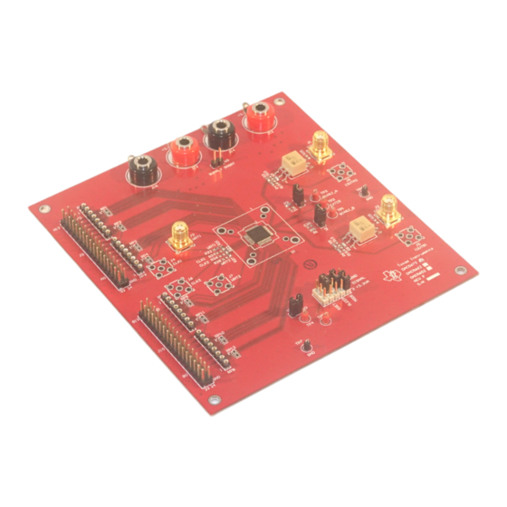
Chapter 3 Physical Description and Parts List This chapter describes the physcial characteristics and the PCB layout of the EVM and lists the components used on the module. Topic Page PCB Layout ..........Parts List . - Page 18 PCB Layout 3.1 PCB Layout The EVM is constructed on a 4-layer, 5.1-inch x 4.8-inch, 0.062-inch thick PCB using FR−4 material. Figure 3−1 through Figure 3−4 show the PCB layout for the EVM. Figure 3−1. Top Layer 1...
- Page 19 PCB Layout Figure 3−2. Layer 2, Ground Plane Physical Description and Parts List...
- Page 20 PCB Layout Figure 3−3. Layer 3, Power Plane...
- Page 21 PCB Layout Figure 3−4. Layer 4, Bottom Layer Physical Description and Parts List...
-
Page 22: Parts List
Parts List 3.2 Parts List Table 3−1 lists the parts used in constructing the EVM. Table 3−1. DAC5672/62/52 EVM Parts List Value Part Number Vendor Ref Des Not Installed Capacitors 47 µF, tantalum, 10%, 10 V 10TPA47M Sanyo C16, C17 10 µF, 10 V, 10% capacitor... -
Page 23: Schematics
Chapter 4 Schematics The following pages contain the schematics for the EVM. Schematics... - Page 24 (SH 2) MODE SLEEP (SH 2) .1uF 10uF DA13 DA13 (MSB) (LSB)DB0 DA12 DA12 DA11 DA11 DA10 DA10 +3.3VA DAC5672/62/52 (Note 1) (Note 1) DB10 DB10 DB11 IOUTB DB11 (Note 1) 49.9 +3.3VB T1-1T DB12 DB13 DB(0..13) 49.9 (SH 2) DB(0..13)
- Page 25 RP12 + C11 34PIN_IDC DB(0..13) 47 uF (SH 1) 10uF 0.01uF DB(0..13) BLACK 12500 TI Boulevard. Dallas, Texas 75243 Title: DAC5672/62/52 Engineer: TENYU DOCUMENTCONTROL # NOTE 1. DO NOT INSTALL REV: Drawn By: Y. DEWONCK FILE: DATE: 16-Mar-2005 SIZE: SHEET:...
Need help?
Do you have a question about the DAC5672 and is the answer not in the manual?
Questions and answers