Table of Contents
Advertisement
Quick Links
Advertisement
Table of Contents

Subscribe to Our Youtube Channel
Related Manuals for EUROCOM W110ER


Summary of Contents for EUROCOM W110ER
- Page 1 All manuals and user guides at all-guides.com W110ER/W110ERF...
- Page 2 All manuals and user guides at all-guides.com...
- Page 3 All manuals and user guides at all-guides.com Preface Notebook Computer W110ER/W110ERF Service Manual...
- Page 4 All manuals and user guides at all-guides.com Preface Notice The company reserves the right to revise this publication or to change its contents without notice. Information contained herein is for reference only and does not constitute a commitment on the part of the manufacturer or any subsequent ven- dor.
- Page 5 This manual is intended for service personnel who have completed sufficient training to undertake the maintenance and inspection of personal computers. It is organized to allow you to look up basic information for servicing and/or upgrading components of the W110ER/ W110ERF series notebook PC.
- Page 6 All manuals and user guides at all-guides.com Preface IMPORTANT SAFETY INSTRUCTIONS Follow basic safety precautions, including those listed below, to reduce the risk of fire, electric shock and injury to per- sons when using any electrical equipment: 1. Do not use this product near water, for example near a bath tub, wash bowl, kitchen sink or laundry tub, in a wet basement or near a swimming pool.
- Page 7 All manuals and user guides at all-guides.com Preface Instructions for Care and Operation The notebook computer is quite rugged, but it can be damaged. To prevent this, follow these suggestions: 1. Don’t drop it, or expose it to shock. If the computer falls, the case and the components could be damaged. Do not expose the computer Do not place it on an unstable Do not place anything heavy...
- Page 8 All manuals and user guides at all-guides.com Preface 4. Avoid interference. Keep the computer away from high capacity transformers, electric motors, and other strong mag- netic fields. These can hinder proper performance and damage your data. 5. Take care when using peripheral devices. Use only approved brands of Unplug the power cord before peripherals.
- Page 9 All manuals and user guides at all-guides.com Preface Battery Precautions • Only use batteries designed for this computer. The wrong battery type may explode, leak or damage the computer. • Do not continue to use a battery that has been dropped, or that appears damaged (e.g. bent or twisted) in any way. Even if the computer continues to work with a damaged battery in place, it may cause circuit damage, which may possibly result in fire.
- Page 10 All manuals and user guides at all-guides.com Preface Related Documents You may also need to consult the following manual for additional information: User’s Manual on DVD This describes the notebook PC’s features and the procedures for operating the computer and its ROM-based setup pro- gram.
- Page 11 All manuals and user guides at all-guides.com Preface System Startup 1. Remove all packing materials. 2. Place the computer on a stable surface. 3. Insert the battery and make sure it is locked in position. 4. Attach the AC/DC adapter to the DC-In jack on the left of the computer, then plug the AC power cord into an outlet, and connect the AC power cord to the AC/DC adapter.
- Page 12 All manuals and user guides at all-guides.com Preface...
-
Page 13: Table Of Contents
All manuals and user guides at all-guides.com Preface Contents Introduction ..........1-1 LCD ....................A-6 HDD ....................A-7 Overview ..................1-1 Schematic Diagrams......... B-1 Specifications ..................1-2 External Locator - Top View with LCD Panel Open ......1-4 System Block Diagram ..............B-2 External Locator - Front & Right Side Views .........1-5 Processor 1/7 - DMI, FDI, PEG ............B-3 External Locator - Left Side &... - Page 14 All manuals and user guides at all-guides.com Preface CCD, TPM, MULTI CON ............B-29 USB3.0 ..................B-30 Card Reader, LAN (RTL8411) ............ B-31 LED, USB CHARGE ..............B-32 HDMI, RJ45 ................. B-33 AUDIO CODEC VT1802P ............B-34 KBC-ITE IT8518E ............... B-35 5VS, 3VS, 3.3VM, 1.5VS CPU ...........
-
Page 15: Introduction
Chapter 1: Introduction Overview This manual covers the information you need to service or upgrade the W110ER/W110ERF series notebook computer. Information about operating the computer (e.g. getting started, and the Setup utility) is in the User’s Manual. Information about dri-vers (e.g. VGA & audio) is also found in the User’s Manual. The manual is shipped with the computer. -
Page 16: Specifications
All manuals and user guides at all-guides.com Introduction Specifications Processor Memory Intel® Core™ i7 Processor Two 204 Pin SO-DIMM Sockets Supporting DDR3 1333/ 1600MHz Memory i7-3612QM (2.10GHz) Memory Expandable up to 8GB 6MB L3 Cache, 22nm, DDR3-1600MHz, TDP 35W i7-3520M (2.90GHz) (The real memory operating frequency depends on the FSB Latest Specification Information... - Page 17 All manuals and user guides at all-guides.com Introduction Security Communication Kensington Lock Slot Built-In Gigabit Ethernet LAN BIOS Password (Factory Option) 1.3M Pixel USB PC Camera Module Interface WLAN/ Bluetooth Half Mini-Card Modules: (Factory Option) Intel® Centrino® Advanced-N 6235 Wire- One Powered USB 2.0 Port less LAN (802.11a/g/n) + Bluetooth 4.0 Two USB 3.0 Ports...
-
Page 18: External Locator - Top View With Lcd Panel Open
All manuals and user guides at all-guides.com Introduction External Locator - Top View with LCD Panel Open Figure 1 Top View 1. Built-In PC Camera 2. Built-In Microphone 3. LCD 4. LED Indicators 5. Power Button 6. Keyboard 7. Touchpad & Buttons 1 - 4 External Locator - Top View with LCD Panel Open... -
Page 19: External Locator - Front & Right Side Views
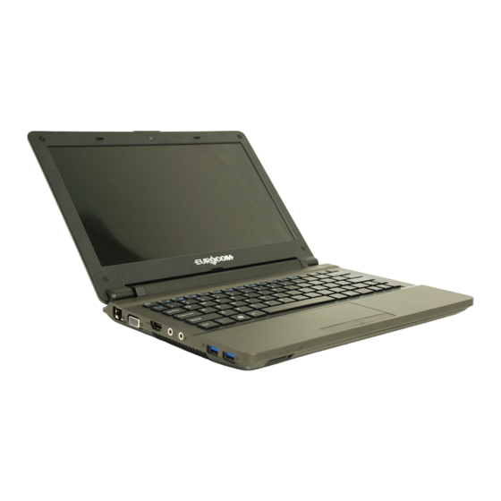
All manuals and user guides at all-guides.com Introduction External Locator - Front & Right Side Views Figure 2 Front View 1. LED Indicators 2. Multi-In-1 Card Reader FRONT VIEW Figure 3 RIGHT SIDE VIEW Right Side View 1. Security Lock Slot 2. -
Page 20: External Locator - Left Side & Rear View
All manuals and user guides at all-guides.com Introduction External Locator - Left Side & Rear View Figure 4 Left Side View 1. RJ-45 LAN Jack 2. External Monitor Port LEFT SIDE VIEW 3. HDMI-Out Port 4. Headphone-Out Jack 5. Microphone-In Jack 6. -
Page 21: External Locator - Bottom View
All manuals and user guides at all-guides.com Introduction External Locator - Bottom View Figure 6 Bottom View 1. Battery 2. Speakers 3. Fan Intake/Vent 4. Multi-In-1 Card Reader Overheating To prevent your com- puter from overhea- ting, make sure no- thing blocks any vent while the computer is in use. -
Page 22: Mainboard Overview - Top (Key Parts)
All manuals and user guides at all-guides.com Introduction Mainboard Overview - Top (Key Parts) Figure 7 Mainboard Top Key Parts 1. Audio Codec 2. TI USB 3.0 3. TPM 1 - 8 Mainboard Overview - Top (Key Parts) -
Page 23: Mainboard Overview - Bottom (Key Parts)
All manuals and user guides at all-guides.com Introduction Mainboard Overview - Bottom (Key Parts) Figure 8 Mainboard Bottom Key Parts 1. Mini-Card Connector (WLAN Module) 2. CPU Socket 3. Memory Slot DDR3 SO-DIMM 4. Intel PCH 5. Card Reader Socket 6. -
Page 24: Mainboard Overview - Top (Connectors)
All manuals and user guides at all-guides.com Introduction Mainboard Overview - Top (Connectors) Figure 9 Mainboard Top Connectors 1. Keyboard Cable Connector 2. Touchpad Connector 3. Power Switch Connector 4. HDMI-Out Port 5. Headphone-Out Jack 6. Microphone-In Jack 1 - 10 Mainboard Overview - Top (Connectors) -
Page 25: Mainboard Overview - Bottom (Connectors)
All manuals and user guides at all-guides.com Introduction Mainboard Overview - Bottom (Connectors) Figure 10 Mainboard Bottom Connectors 1. DC-In Jack 2. USB 2.0 Ports 3. CMOS Battery Connector 4. Fan Cable Connector 5. USB Port 6. LVDS Cable Connector 7. - Page 26 All manuals and user guides at all-guides.com Introduction 1 - 12...
-
Page 27: Disassembly
Chapter 2: Disassembly Overview This chapter provides step-by-step instructions for disassembling the W110ER/W110ERF series notebook’s parts and subsystems. When it comes to reassembly, reverse the procedures (unless otherwise indicated). We suggest you completely review any procedure before you take the computer apart. -
Page 28: Maintenance Tools
All manuals and user guides at all-guides.com Disassembly NOTE: All disassembly procedures assume that the system is turned OFF, and disconnected from any power supply (the battery is removed too). Maintenance Tools The following tools are recommended when working on the notebook PC: •... -
Page 29: Maintenance Precautions
All manuals and user guides at all-guides.com Disassembly Maintenance Precautions The following precautions are a reminder. To avoid personal injury or damage to the computer while performing a re- moval and/or replacement job, take the following precautions: Power Safety Warning 1. -
Page 30: Disassembly Steps
All manuals and user guides at all-guides.com Disassembly Disassembly Steps The following table lists the disassembly steps, and on which page to find the related information. PLEASE PERFORM THE DISASSEMBLY STEPS IN THE ORDER INDICATED. To remove the Battery: To remove the Keyboard: 1. -
Page 31: Removing The Battery
All manuals and user guides at all-guides.com Disassembly Removing the Battery 1. Turn the computer off, and turn it over. Figure 1 2. Slide the latch in the direction of the arrow (Figure 1a Battery Removal 3. Slide the latch in the direction of the arrow, and hold it in place (Figure 1a 4. -
Page 32: Removing The Cmos Battery
All manuals and user guides at all-guides.com Disassembly Removing the CMOS Battery Figure 2 CMOS battery 1. Turn off the computer, remove the battery (page 2 - Assembly Removal 2. Slide the latch in the direction of the arrow, and hold it in place (Figure 2a 3. -
Page 33: Removing The Hard Disk Drive
All manuals and user guides at all-guides.com Disassembly Removing the Hard Disk Drive Figure 3 HDD Assembly The hard disk drive can be taken out to accommodate other 2.5" serial (SATA) hard disk drives with a height of 9.5mm Removal (h) and a speed of 5400 RPM or lower. - Page 34 All manuals and user guides at all-guides.com Disassembly 4. Grip the mylar cover and slide the hard disk in the direction of arrow (Figure 4b Figure 4 5. Lift the hard disk assembly out of the bay (Figure 4c HDD Assembly 6.
-
Page 35: Removing And Installing A Processor
All manuals and user guides at all-guides.com Disassembly Removing and Installing a Processor Figure 5 Processor Removal Processor Removal Procedure 1. Turn off the computer, remove the battery (page 2 - 5) and the component bay cover (page 2 - 12). - Page 36 All manuals and user guides at all-guides.com Disassembly 5. Turn the release latch towards the unlock symbol , to release the CPU (Figure 6d). Figure 6 6. Carefully (it may be hot) lift the CPU up out of the socket (Figure 6e).
- Page 37 All manuals and user guides at all-guides.com Disassembly Processor Installation Procedure Figure 7 1. Insert the CPU (Figure 7a), pay careful attention to the pin alignment, it will fit only one way (DO NOT FORCE Processor Installation IT!), and turn the release latch towards the lock symbol (Figure 7b).
-
Page 38: Removing The System Memory (Ram)
All manuals and user guides at all-guides.com Disassembly Removing the System Memory (RAM) Figure 8 RAM Module The computer has two memory sockets for 200 pin Small Outline Dual In-line Memory Modules (SO-DIMM) supporting Removal DDRIII (DDR3) Up to 1333/1600MHz. The main memory can be expanded up to 8GB. The SO-DIMM modules sup- ported are 1024MB and 2048MB DDRIII Modules. - Page 39 All manuals and user guides at all-guides.com Disassembly 6. Insert a new module holding it at about a 30° angle and fit the connectors firmly into the memory slot. Figure 9 7. The module will only fit one way as defined by its pin alignment. Make sure the module is seated as far into the slot RAM Module as it will go.
-
Page 40: Removing The Wireless Lan Module
All manuals and user guides at all-guides.com Disassembly Removing the Wireless LAN Module Figure 10 Wireless LAN 1. Turn off the computer, remove the battery (page 2 - 5) and the component bay cover (page 2 - Module Removal 2. The Wireless LAN module will be visible at point (Figure 10a on the mainboard. -
Page 41: Removing The Keyboard
All manuals and user guides at all-guides.com Disassembly Removing the Keyboard Figure 11 Keyboard Removal 1. Turn off the computer and remove the battery (page 2 - 2. Use only the small tool provided (see picture below) to carefully press the four keyboard latches at the a. - Page 42 All manuals and user guides at all-guides.com Disassembly 2 - 16...
-
Page 43: Part Lists
Part Lists Appendix A:Part Lists This appendix breaks down the W110ER/W110ERF series notebook’s construction into a series of illustrations. The component part numbers are indicated in the tables opposite the drawings. Note: This section indicates the manufacturer’s part numbers. Your organization may use a different system, so be sure to cross-check any relevant documentation. -
Page 44: Parts List Illustration Location
All manuals and user guides at all-guides.com Part Lists Parts List Illustration Location The following table indicates where to find the appropriate parts list illustration. Table A - 1 Parts List Illustration Parts Location page A - 3 page A - 4 Bottom page A - 5 page A - 6... -
Page 45: Top
All manuals and user guides at all-guides.com Part Lists Figure A - 1 Top A - 3... -
Page 46: Bottom
All manuals and user guides at all-guides.com Part Lists Bottom Figure A - 1 Bottom A - 4 Bottom... - Page 47 All manuals and user guides at all-guides.com Part Lists Figure A - 2 MB A - 5...
-
Page 48: Lcd
All manuals and user guides at all-guides.com Part Lists Figure A - 3 A - 6... -
Page 49: Hdd
All manuals and user guides at all-guides.com Part Lists Figure A - 4 HDD A - 7... - Page 50 All manuals and user guides at all-guides.com Part Lists A - 8...
- Page 51 All manuals and user guides at all-guides.com Schematic Diagrams Appendix B: Schematic Diagrams Table B - 1 This appendix has circuit diagrams of the W110ER/W110ERF notebook’s PCB’s. The following table indicates where SCHEMATIC to find the appropriate schematic diagram. DIAGRAMS...
-
Page 52: Schematic Diagrams
All manuals and user guides at all-guides.com Schematic Diagrams System Block Diagram VDD3,VDD5 W110ER 5IN1 6-7P-W1105-001 W110ER Chief River System Block Diagram W110ER MAIN BOARD 6-71-W1100-D02A GPU NVDIDA NVVDD 1067/1333/1600 MHz CLICK BOARD 5V,3V,5VS,3VS,1.5VS, 6-71-W1102-D02 DDR3 / 1.5V PCIE*8 Ivy Bridge +1.5S_CPU... -
Page 53: Processor 1/7 - Dmi, Fdi, Peg
All manuals and user guides at all-guides.com Schematic Diagrams Processor 1/7 - DMI, FDI, PEG Ivy Bridge Processor 1/7 ( DMI,PEG,FDI ) 1.05VS_VTT U 31A 20 mil PEG_IRCOMP_R R 120 24.9_1%_04 PEG_IC OMPI PEG_IC OMPO D MI_TXN0 DMI_R X#[0] PEG_RC OMPO PEG Compensation Signal D MI_TXN1 DMI_R X#[1]... -
Page 54: Processor 2/7 - Clk, Misc
All manuals and user guides at all-guides.com Schematic Diagrams Processor 2/7 - CLK, MISC PU/PD for JTAG signals Ivy Bridge Processor 2/7 ( CLK,MISC,JTAG ) Processor Pull downs 1.05VS_VTT H_CPUPWRGD_R XDP_TMS 10K_04 R343 R361 51_04 XDP_TDI_R R354 51_04 XDP_PREQ# R355 *51_04 TRACE WIDTH 10MIL, LENGTH <500MILS XDP_TDO_R... -
Page 55: Processor 3/7 - Ddr3
All manuals and user guides at all-guides.com Schematic Diagrams Processor 3/7 - DDR3 Ivy Bridge Processor 3/7 ( DDR3 ) U 31C U31D M_A_D Q[63:0] M_A_C LK_DDR 0 9 M_B_DQ[63:0] M_B_C LK_DD R 2 10 SA_C K[0] SB_CK[0] AD 2 M_A_C LK_DDR #0 9 M_B_C LK_DD R #2 10 SA_CLK#[0]... -
Page 56: Processor 4/7 - Power
All manuals and user guides at all-guides.com Schematic Diagrams Processor 4/7 - Power Ivy Bridge Processor 4/7 ( POWER ) POWER U31F PROCESSOR CORE POWER PROCESSOR UNCORE POWER VCORE 1.05VS_VTT 1.05VS_VTT 8.5A AG35 ICCMAX Maximum Processor VCC1 AG34 AH13 VCC2 VCCIO1 AG33 AH10... -
Page 57: Processor 5/7 - Gfx Pwr
All manuals and user guides at all-guides.com Schematic Diagrams Processor 5/7 - GFX PWR Ivy Bridge Processor 5/7 ( GRAPHICS POWER ) POWER 1.5VS_CPU U31G VGFX_CORE AT24 AK35 VCC_GT_SENSE 40 AT23 VAXG1 VAXG_SENSE AK34 R385 0_04 R386 VSS_GT_SENSE 40 VAXG2 VSSAXG_SENSE C182 C168... -
Page 58: Processor 6/7 - Gnd
All manuals and user guides at all-guides.com Schematic Diagrams Processor 6/7 - GND Ivy Bridge Processor 6/7 ( GND ) U31H U31I AT35 AJ22 VSS1 VSS81 AT32 AJ19 VSS2 VSS82 AT29 AJ16 VSS3 VSS83 VSS161 VSS234 AT27 AJ13 VSS4 VSS84 VSS162 VSS235 AT25... -
Page 59: Processor 7/7 - Rsvd
All manuals and user guides at all-guides.com Schematic Diagrams Processor 7/7 - RSVD Ivy Bridge Processor 7/7 ( RESERVED ) CFG Straps for Processor PEG Static Lane Reversal - CFG2 is for the 16x 1:(Default) Normal Operation; Lane # CFG2 definition matches socket pin map definition 0:Lane Reversed C FG2... -
Page 60: Ddr3 So-Dimm_0
All manuals and user guides at all-guides.com Schematic Diagrams DDR3 SO-DIMM_0 SO-DIMM A C307 *10p_50V_NPO_04 M_A_CLK_DDR0 M_A_CLK_DDR#0 JDIMM1A M_A_A[15:0] M_A_DQ[63:0] 4 M_A_A0 M_A_DQ0 C300 *10p_50V_NPO_04 JDIMM1B M_A_CLK_DDR1 M_A_CLK_DDR#1 M_A_A1 M_A_DQ1 M_A_A2 M_A_DQ2 M_A_A3 M_A_DQ3 1.5V M_A_A4 M_A_DQ4 M_A_A5 M_A_DQ5 VDD1 VSS16 M_A_A6 M_A_DQ6... -
Page 61: Ddr3 So-Dimm_1
All manuals and user guides at all-guides.com Schematic Diagrams DDR3 SO-DIMM_1 SO-DIMM B JDIMM2B C357 *10p_50V_NPO_04 M_B_CLK_DDR2 M_B_CLK_DDR#2 1.5V JDIMM2A M_B_A[15:0] M_B_DQ[63:0] 4 C347 *10p_50V_NPO_04 M_B_A0 M_B_DQ0 M_B_CLK_DDR3 M_B_CLK_DDR#3 M_B_A1 M_B_DQ1 VDD1 VSS16 M_B_A2 M_B_DQ2 VDD2 VSS17 M_B_A3 M_B_DQ3 VDD3 VSS18 M_B_A4 M_B_DQ4... -
Page 62: Panel, Inverter, Crt
All manuals and user guides at all-guides.com Schematic Diagrams PANEL, INVERTER, CRT PANEL CONNECTOR PJ29 PJ29»Ýµu¸ô OPEN_2A VIN_LCD *P2003EVG PLVDD 3.3VS 7/11 PIN DefineÅܧó(Follow¦@¥Î½u¸ô0622) 3.3V C107 *0.22u_50V_Y5V_06 C500 C491 J_LCD1 0.1u_16V_Y5V_04 3.3VS *4.7K_04 4.7u_6.3V_X5R_06 0.1u_16V_Y5V_04 *1M_04 2.2K_04 2.2K_04 *100K_04 *10K_04 LVDS-LCLKN P_DDC_CLK P_DDC_CLK 21... -
Page 63: Vga Pci-E Interface
All manuals and user guides at all-guides.com Schematic Diagrams VGA PCI-E Interface 3.3VS Term Description 1u_6.3V_X5R_04 MC74VHC1G08DFT2G The total trace length measured from GPU ball to capacitor is Under GPU no more than 150 mil dGPU_RST# PERSTB# The total trace length measured from GPU ball to capacitor is no Near GPU U27P... -
Page 64: Vga Frame Buffer Interface
All manuals and user guides at all-guides.com Schematic Diagrams VGA Frame Buffer Interface Frame Buffer Interface Term Description The total trace length measured U27C from GPU ball to capacitor is Under GPU no more than 150 mil bga_0908_p080_p085_p100_290x290 The total trace length measured U27B COMMON from GPU ball to capacitor is no... -
Page 65: Vga Frame Buffer A
All manuals and user guides at all-guides.com Schematic Diagrams VGA Frame Buffer A Term Description Frame Buffer Partition A The total trace length measured from GPU ball to capacitor is Under GPU no more than 150 mil FBA_CMD[31: 0] The total trace length measured FBA_CMD[31:0] from GPU ball to capacitor is no Near GPU... -
Page 66: Vga Frame Buffer C
All manuals and user guides at all-guides.com Schematic Diagrams VGA Frame Buffer C Frame Buffer Partition C Term Description The total trace length measured from GPU ball to capacitor is PLACE UNDER BALLS FBVDDQ Under GPU no more than 150 mil FBVDDQ The total trace length measured from GPU ball to capacitor is no... -
Page 67: Vga I/O
All manuals and user guides at all-guides.com Schematic Diagrams VGA I/O U27M Term Description bga_0908_p080_p085_p100_290x290 R364 *10mil_short_04 VGA_THERM_SHDWN_# COMMON The total trace length measured 9/19 IFPEF from GPU ball to capacitor is Under GPU no more than 150 mil THERM# ALL PINS NC FOR GF117 VGA_THERM_SHDWN# VGA_THERMDC... -
Page 68: Vga Nvvdd Cecoupling
All manuals and user guides at all-guides.com Schematic Diagrams VGA NVVDD Cecoupling U27G U27I U27E bga_0908_p080_p085_p100_290x290 PLACE UNDER GPU bga_0908_p080_p085_p100_290x290 NVVDD bga_0908_p080_p085_p100_290x290 COMMON COMMON COMMON 14/19 NVVDD 17/19 GND_2/2 16/19 G ND_1/2 AM25 AA12 AA17 AA14 AA18 AN10 AA16 AA20 AN13 AA19 AA22... -
Page 69: Pch 1/9 - Rtc, Hda, Sata
All manuals and user guides at all-guides.com Schematic Diagrams PCH 1/9 - RTC, HDA, SATA NO REBOOT STRAP RTCVCC PantherPoint - M (RTC,HDA,SATA) NO REBOOT STRAP: HDA_SPKR High Enable BAT54CW(lision) 3.3VS 20mils 20mils VDD3 C440 SERIRQ C650 1u_6.3V_X5R_04 18p_50V_NPO_04 10K_04 R436 RTC_VBAT_1 HDA_SPKR... -
Page 70: Pch 2/9 - Pcie, Smbus, Clk
All manuals and user guides at all-guides.com Schematic Diagrams PCH 2/9 - PCIE, SMBUS, CLK PantherPoint - M (PCI-E,SMBUS,CLK) 3.3V U20B RN16 2.2K_8P4R_04 BG34 SMB_CLK PERN1 BJ34 BT_SBD# SMB_DATA PERP1 SMBALERT# / GPIO11 BT_SBD# 27 AV32 SML0_CLK PETN1 AU32 SMB_CLK SML0_DATA SMB_CLK 9,10 PETP1... -
Page 71: Pch 3/9 - Dmi, Fdi, Pwrgd
All manuals and user guides at all-guides.com Schematic Diagrams PCH 3/9 - DMI, FDI, PWRGD PantherPoint -M (DMI,FDI,GPIO) U20C BC24 BJ14 FDI_TXN 0 2 DMI_R XN0 DMI0RXN FD I_R XN 0 BE20 AY 14 3.3V FDI_TXN 1 2 DMI_R XN1 DMI1RXN FD I_R XN 1 BG18... -
Page 72: Pch 4/9 - Lvds, Ddi, Crt
All manuals and user guides at all-guides.com Schematic Diagrams PCH 4/9 - LVDS, DDI, CRT PantherPoint -M (LVDS,DDI) U20D AP43 BLON L_BKLTEN SDVO_TVCLKINN AP45 11,34 NB_ENAVDD L_VDD_EN SDVO_TVCLKINP AM42 L_BKLTCTL SDVO_STALLN AM40 SDVO_STALLP Ver:1.0 P_DDC_CLK L_DDC_CLK AP39 3.3VS pull up 2.2K P_DDC_DATA L_DDC_DATA SDVO_INTN... -
Page 73: Pch 5/9 - Pci, Usb, Rsvd
All manuals and user guides at all-guides.com Schematic Diagrams PCH 5/9 - PCI, USB, RSVD PantherPoint -M (PCI,USB,RSVD) 3.3V RN18 10K_8P4R_04 USB_OC#23 U20E USB_OC#89 USB_OC#1213 RSVD1 USB_OC#45 RSVD2 BG26 RSVD3 BJ26 RN17 RSVD4 BH25 10K_8P4R_04 BJ16 AT10 USB_OC#1011 Boot BIOS Strap RSVD5 BG16 USB_OC#14... -
Page 74: Pch 6/9 - Gpio, Cpu
All manuals and user guides at all-guides.com Schematic Diagrams PCH 6/9 - GPIO, CPU 3.3V PantherPoint - M (GPIO,VSS_NCTF,RSVD) R275 1K_04 HOST_ALERT#1 HOST_ALERT#2 R474 1K_04 R482 *10K_04 TEST_DET R450 *10K_04 PLL_ODVR_EN 3.3VS GPIO34 R269 *1K_04 U20F R478 *10K_04 DGPU_PWROK R284 1K_04 GPIO68 S_GPIO... -
Page 75: Pch 7/9 - Pwr
All manuals and user guides at all-guides.com Schematic Diagrams PCH 7/9 - PWR PantherPoint -M (POWER) 3.3VS HCB1608KF-121T25 POWER U20G 1.05VS VCCA_DAC_3.3VS HCB1608KF-121T25 1.3A AA23 VCCA_DAC3.3VS VCCCORE[1] VCCADAC AC23 VCCCORE[2] AD21 C594 C625 C604 C623 C409 C413 C412 C408 C401 R241 VCCCORE[3] AD23... -
Page 76: Pch 8/9 - Power
All manuals and user guides at all-guides.com Schematic Diagrams PCH 8/9 - POWER PantherPoint - M (POWER) PantherPoint power supply range *HCB1005KF-121T20 Voltage 1.05VS 1.05VS POWER U20J 1.00V 1.05V 1.10V 3.3V AD49 C644 1.43V 1.5V 1.58V VCCACLK VCCIO[29] Note: C636 - UNSTUFF ALWAYS FOR CPT C608 0.1u_10V_X5R_04 1.71V... -
Page 77: Pch 9/9 - Gnd
All manuals and user guides at all-guides.com Schematic Diagrams PCH 9/9 - GND PantherPoint -M (GND) Voltage Rail Voltage S0 Iccmax Current (A) U20I V_CPU_IO 1.05 1 (mA) U20H V5REF 1 (mA) VSS[159] VSS[259] VSS[0] AY42 V5REF_Sus 1 (mA) VSS[160] VSS[260] AY46 AA17... -
Page 78: Wlan, 3G, Mini Pcie
All manuals and user guides at all-guides.com Schematic Diagrams WLAN, 3G, MINI PCIE WLAN MINI CARD J_MINI1 M-MARK M-MARK M-MARK M-MARK M-MARK M-MARK M-MARK M-MARK 20 mil WAKE# R278 *0_04 20,29,30 PCIE_WAKE# WAKE# 3.3VAUX_0 3.3V_WLAN COEX1 1.5V_0 20 mil VDD3 COEX2 UIM_PWR R271... -
Page 79: Ccd, Tpm, Multi Con
All manuals and user guides at all-guides.com Schematic Diagrams CCD, TPM, MULTI CON CPU FAN CONTROL FOR POWER SW BOARD 5VS_FAN VOUT 3.3VS 3.3V C422 VSET R690 CPU_FAN 7/11 PIN DefineÅܧó(PIN2§ï¬°GND) 1u_10V_Y5V_06 AX995SA J_SW1 *0_04 5VS_FAN 20mil J_FAN1 CPU_FAN 34 6-02-03940-B20 6-02-00995-B20 MBTN... -
Page 80: Usb3.0
All manuals and user guides at all-guides.com Schematic Diagrams USB3.0 3.3V_USB3 3.3V_USB3 1.1V *HCB1608KF-121T25 C750 C751 C736 C737 C738 C739 C740 C741 C742 C743 C744 C745 C746 C747 C748 C749 3.3V_USB3 3.3V_USB3 1.1V R580 R581 C754 C753 C755 C756 C757 C758 C759 C760... -
Page 81: Card Reader, Lan (Rtl8411
All manuals and user guides at all-guides.com Schematic Diagrams Card Reader, LAN (RTL8411) Switching Regulator close to PIN48 LAN (RTL8411) R661 0_06 VDD10 (>20mil) PULL HIGH: SWR Mode VDD3 Crystal 8045 & 3225 Co-lay RSET R662 2.49K_1%_04 REGOUT VDD10 ENSWREG R663 *0_04 meet realtek Freq tolerance 50ppm... -
Page 82: Led, Usb Charge
All manuals and user guides at all-guides.com Schematic Diagrams LED, USB CHARGE USB Charge Port 3.3VS 3.3VS 3.3VS NUM LOCK CAPS LOCK SCROLL LOCK 220_04 220_04 220_04 VDD5 USBVCC01 RY-SP170Y G34-5M RY -SP170YG34-5M RY -SP170Y G34-5M 10u_10V_Y 5V_08 USB1_PN9 Green Green Green USB_PN9... -
Page 83: Hdmi, Rj45
All manuals and user guides at all-guides.com Schematic Diagrams HDMI, RJ45 LAN PORT HDMIC_C0CP-R TMDS_DATA2-R R306 0_04 R308 0_04 C856 0.1u_10V_X7R_04 HDMIC_C0CP IN_D1+ OUT_D1+ HDMIC_C0CN-R TMDS_DATA2#-R R305 0_04 R307 0_04 C857 0.1u_10V_X7R_04 HDMIC_C0CN IN_D1- OUT_D1- J_RJ_1 LMX1+ DLMX1+ LMX2+ DLMX2+ HDMIC_C1CP-R TMDS_DATA1-R C858... -
Page 84: Audio Codec Vt1802P
All manuals and user guides at all-guides.com Schematic Diagrams AUDIO CODEC VT1802P CODEC (ALC269 & VT1802P) PVDD1_2 R154 Layout note: *15mil_short_06 EMI Require GND and AUDG space is 60mils ~ 100mils C278 0.1u_16V_Y5V_04 C250 C228 10u_10V_Y5V_08 C802 0.1u_16V_Y 5V_04 C213 0.1u_16V_Y5V_04 0.1u_16V_Y5V_04 *10mil_short_04... -
Page 85: Kbc-Ite It8518E
All manuals and user guides at all-guides.com Schematic Diagrams KBC-ITE IT8518E KBC_AVDD 7/11 ¤¸¥óÅܧó(§ï¬°0805) HCB1005KF-121T20 VDD3 VDD3 Board-n¥[ VDD3 C392 C353 C592 C579 C365 C364 C580 0.1u_16V_Y 5V_04 10u_10V_Y 5V_08 0.1u_16V_Y 5V_04 0.1u_16V_Y 5V_04 0.1u_16V_Y 5V_04 *0.1u_16V_Y 5V_04 *0.1u_16V_Y 5V_04 R400 EC MODULE CHOOSE () C586... -
Page 86: 5Vs, 3Vs, 3.3Vm, 1.5Vs Cpu
All manuals and user guides at all-guides.com Schematic Diagrams 5VS, 3VS, 3.3VM, 1.5VS CPU VDD3 VDD3 PC153 PC56 PC42 PC64 PR151 PR157 VIN1 VIN1 *12K_04 10K_04 PR132 PR156 100K_04 DD_ON DD_ON_LATCH 10K_04 PR155 1K_04 PWR_SW#_R PR163 1K_04 PWR_SW# M_BTN# PWR_SW# 34 M_BTN# PWR_SW# DD_ON#... -
Page 87: Vdd3, Vdd5
All manuals and user guides at all-guides.com Schematic Diagrams VDD3, VDD5 VREF_VDD PR113 *0_04 PR114 0_04 PC71 1u_10V_Y 5V_06 VFB2 VFB1 PR259 PR257 EN_3V EN_5V PC72 100K_04 100K_04 PC74 1000p_50V_X7R_04 1000p_50V_X7R_04 VREG3 PC87 PC205 PC75 PR116 *10K_04 SYS5V VDD3 LDO3 VDD5 1u_10V_Y 5V_06 PC207... -
Page 88: Power 0.85Vs, 1.8Vs
All manuals and user guides at all-guides.com Schematic Diagrams Power 0.85VS, 1.8VS PEX_VDD NM OS 1.05VS PQ34 -n²¾¾aªñPIN6¸} SY S15V ME4626-G PEX_VDD 1.05V@4A 1.8VS 3.3 V 250 MIL PC199 PR147 V1.8 PC111 PC112 PU12 2.2u_6.3V_X5R_06 1.8VS 1M_04 PR149 PR253 10K_04 3.3V VCNTL 1.05V_PWR_EN... -
Page 89: Power 1.5V
All manuals and user guides at all-guides.com Schematic Diagrams POWER 1.5V PD12 PC 214 PC97 PC99 PC215 PQ62 ME4894-G RB0540S2 PU13 VTT_MEM VD DQ PC217 1.5V 10u_6.3V_X5R_06 VBST PC107 0.1u_10V_X7R_04 VLDOIN VBST VDDQ PJ22 PR267 D RVH 7/13 PQ62,PQ63,PQ64 footprintÅܧó TMPC1004H-R56M-Z01 PJ19 VTT_MEM... -
Page 90: Power 1.05Vs/1.05Vs Vtt
All manuals and user guides at all-guides.com Schematic Diagrams POWER 1.05VS/1.05VS VTT 1.05VS EMI PW PLANT PD11 PC244 PC245 PC243 PR129 1.05V_ON RB0540S2 PC236 PC225 PC228 PC237 PR265 5.1K_1%_04 100K_04 PQ28 MTN7002ZHS3 PQ69 ME4894-G 35,37,38 SUSB G5413 PC94 0.47u_10V_X5R_04 1.05VS PC95 V1.05 0.1u_10V_X7R_04... -
Page 91: Power Vcore1
All manuals and user guides at all-guides.com Schematic Diagrams POWER VCORE1 PC19 680p_50V_X7R_04 1.05VS_VTT PR30 PR209 VCORE_1 CLOSE TO VR 10_04 1.2k_1%_04 B~4350 PUT COLSE PR37 PR228 PR217 PC18 PRT1 TO VCORE 24.9K_1%_04 130_1%_04 54.9_1%_04 3300p_50V_X7R_04 Phase 1 A_GND Inductor H_CPU_SVIDDAT H_CPU_SVIDDAT 100K_NTC_06_B... -
Page 92: Power Vcore2
All manuals and user guides at all-guides.com Schematic Diagrams POWER VCORE2 VCORE_2 PC10 PC11 PC137 PR200 2.2_06 PC161 0.22u_10V_X7R_06 P/N: 6-09-33712-142 NTMFS4926N NTMFS4926N NCP5911 PU10 VREG_SW1_HG PR343 0_06 VCORE TMPB1235MP-R36M-Z01 VREG_SW1_OUT VR1_PWM1 PW M PQ48 PQ42 PQ51 PR199 NTMFS4935N NTMFS4935N NTMFS4935N PD13 DRON... -
Page 93: Power Vga Nvvdd
All manuals and user guides at all-guides.com Schematic Diagrams Power VGA NVVDD VGA__NVVDD PC254 PC267 SGND2 *1n_50V_04 1u_6.3V_X5R_04 NVVDD PR296 ADP3212_CSREF PR333 *47K_04 *10mil_short CS_PH1 PR294 226K_1%_06 PC302 PC303 CS_PH2 PR287 226K_1%_06 PC24 PC179 PC21 PC22 PC23 PC253 PC287 PC288 PC289 PC290 PR337... -
Page 94: Ac In, Charger
All manuals and user guides at all-guides.com Schematic Diagrams AC IN, CHARGER PR154 0_04 PR162 *470K_04 PQ37 V_BAT MEP4435Q8 V_BAT J_DC_JACK1 ¾aªñJBATTA1 50932-00301-001 PQ33 8.2UH_7.3*6.6*2.8MM HCB4532K-800T90 MEP4435Q8 PQ36A PC108 PR148 7/14 ValueÅܧó PD1503YVS PQ36B PR168 PC291 PC293 PC292 0.01_1%_32 PD1503YVS BCIHP-0730 8R2M 0.01_1%_32 GND1... -
Page 95: Click Board
All manuals and user guides at all-guides.com Schematic Diagrams CLICK BOARD CLICK BOARD 0.1u_16V_Y 5V_04 C5VS Sheet 44 of 48 CJ_TP2 CGND CJ_TP1 C5VS CLICK BOARD CTP_CLK CTP_DATA CTP_DATA CTP_CLK CTPBUTTON_L CTPBUTTON_R *0.1u_16V_Y 5V_04 85201-04051 85201-06051 CGND CGND CGND 6-20-94A50-104 6-20-94AA0-104 6-21-91A00-106 6-20-94A70-104... -
Page 96: Power Sw Board
All manuals and user guides at all-guides.com Schematic Diagrams POWER SW BOARD POWER SW Board S_3.3VS S_3.3VS POWER SWITCH SR 2 220_04 220_04 Z4302 20mil Z4301 6-53-3050B-241 S_3.3VS S_3.3V POWER BUTTON 0.1u_16V_Y 5V_04 0.1u_16V_Y 5V_04 SD 1 SJ_SW 1 SMGND SPW R_SW 2 20mil SM_BTN#... -
Page 97: Hdd Board
All manuals and user guides at all-guides.com Schematic Diagrams HDD BOARD HJ_HDD1 H_5VS HSATA_TXP1_RR 0.01u_16V_X7R_04 HSATA_TXP1_R HJ_SATA1 HSATA_TXN1_RR HSATA_TXN1_R HSATA_RXP1_R 0.01u_16V_X7R_04 HSATA_RXN1_R HSATA_RXN1_RR HSATA_RXN1_R 0.01u_16V_X7R_04 HSATA_RXP1_RR 0.01u_16V_X7R_04 HSATA_RXP1_R HSATA_TXN1_R H_3.3VS HSATA_TXP1_R H_3.3VS POT-12RX-X-XX_A HC10 HC11 HGND HGND Sheet 46 of 48 *0.1u_16V_Y 5V_04 *1u_6.3V_Y5V_04 *10u_6.3V_X5R_06... -
Page 98: Power Diagram
All manuals and user guides at all-guides.com Schematic Diagrams Power Diagram 3.3V 1.05VS 2.92A PWR SW B'd M_BTN# RTCVCC 3.3VS VCORE 1.05VS_VTT 1.5VS 1.05VS_VTT Cougar 8.5A 3.3VS VDD3 Point VGFX_CORE 1.5V ALL_SYS_PWRGD RSMRST# SO-DIMM 1.8VS RSMRST#, PMSYS_PWRGD_BUF 1.2A PWR_SW# DRAMPWROK DPWROK SM_DRAMPWROK IT8518... -
Page 99: Power On Seq
All manuals and user guides at all-guides.com Schematic Diagrams Power On SEQ PWR_SW# 160ms PWR_SW# (PU6.6) DD_ON 211ms DD_ON (PQ27.2) 700us 3.3V rise time=801.32us 3.3V 3.3V (PQ67.1,2) 2.35ms 5V rise time=1.106ms (PQ71.1,2) 226ms RSMRST# RSMRST# (U16.35) PWR_BTN# 55ms 203ms PWR_BTN# (U16.33) 331ms SUSC#... - Page 100 All manuals and user guides at all-guides.com Schematic Diagrams B - 50...
-
Page 101: Updating The Flash Rom Bios
All manuals and user guides at all-guides.com BIOS Update Appendix C:Updating the FLASH ROM BIOS BIOS Version To update the FLASH ROM BIOS, you must: Make sure you down- • Download the BIOS update from the web site. load the latest correct version of the BIOS ap- •... -
Page 102: Use The Flash Tools To Update The Bios
All manuals and user guides at all-guides.com BIOS Update Use the flash tools to update the BIOS 1. Make sure you are not loading any memory management programs such as HIMEM by holding the F8 key as you see the message “Starting MS-DOS”. You will then be prompted to give “Y” or “N” responses to the programs being loaded by DOS.
Need help?
Do you have a question about the W110ER and is the answer not in the manual?
Questions and answers