
Subscribe to Our Youtube Channel
Related Manuals for Cypress CY3677


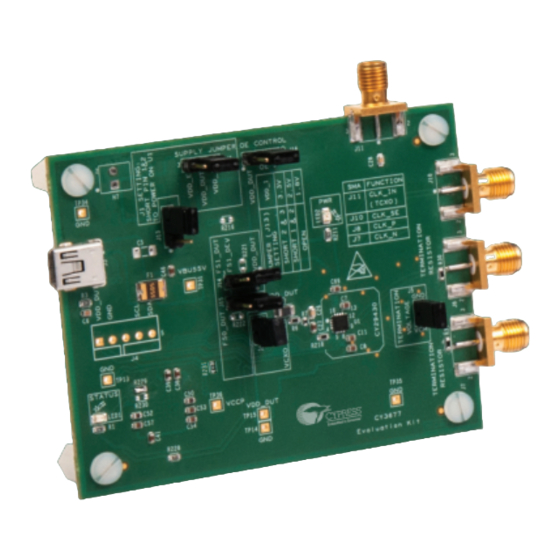
Summary of Contents for Cypress CY3677
- Page 1 CY3677 Evaluation Kit User Guide Doc. No. 002-12185 Rev. *D Cypress Semiconductor 198 Champion Court San Jose, CA95134-1709 Phone (USA): 800.858.1810 Phone (Intnl): +1.408.943.2600 www.cypress.com...
- Page 2 A critical component is any component of a device or system whose failure to perform can be reasonably expected to cause the failure of the device or system, or to affect its safety or effectiveness. Cypress is not liable, in whole or in part, and you shall and hereby do release Cypress from any claim, damage, or other liability arising from or related to all Unintended Uses of Cypress products.
-
Page 3: Table Of Contents
TCXO Input Reference ........................... 24 4.2.7 Frequency Select (FS) ..........................24 Evaluating Different I/O Standards Using the CY3677 EVK ................25 Example Projects ................................. 27 Example Project Configuration Details ........................ 27 CY3677 Evaluation Kit User Guide, Doc. No. 002-12185 Rev. *D... - Page 4 B.2. Termination Settings of LVCMOS Clock Output ....................35 B.3. Schematics ................................36 B.4. Fabrication Drawing ............................. 40 B.5. Bill of Materials ..............................41 Revision History ................................... 44 Document Revision History ............................44 CY3677 Evaluation Kit User Guide, Doc. No. 002-12185 Rev. *D...
-
Page 5: Safety Information
Handling Boards The CY3677 Evaluation Kit is sensitive to ESD. Hold the board only by its edges. After removing the board from its box, place it on a grounded, static-free surface. Use a conductive foam pad if available. Do not slide the board over any surface. -
Page 6: Introduction
1 Introduction Thank you for your interest in the CY3677 Evaluation Kit (EVK). The CY3677 EVK is designed to enable you to evaluate the programmable clock device CY29430, the latest addition to the Cypress timing product portfolio. The clock device CY29430 is a high-performance programmable oscillator with one fractional PLL that generates any frequency up to 2.1 GHz with jitter... -
Page 7: Getting Started
1.2 Getting Started To learn the solution quickly and apply it to your design, refer to the CY3677 Quick Start Guide inside the kit box or in the installation directory. The default location for the kit documents is: <Install_Directory>\CY3677 Evaluation Kit\<version>\Documentation... -
Page 8: Document Conventions
Low Voltage Positive Emitter Coupled Logic with zero Common-mode current LVDS Low Voltage Differential Signaling Output Enable Third Overtone Crystal Subminiature Version A VCXO Voltage-Controlled Crystal Oscillator TCXO Temperature Compensated Crystal Oscillator One-Time Programmable CY3677 Evaluation Kit User Guide, Doc. No. 002-12185 Rev. *D... -
Page 9: Software Installation
2 Software Installation This chapter describes the steps to install the software tools and packages on a PC for using the CY3677 Evaluation Kit. 2.1 Before You Begin All Cypress software installations require administrator privileges. Ensure that you have the required privileges on the system for successful installation. - Page 10 Software Installation Figure 2-1. Installer Screen Click Change… if you want to install the CY3677 EVK in a location other than the default, and then click Next as shown Figure 2-2. Note: When you click Next, the CY3677 EVK installer automatically installs the required software, if it is not present on your computer.
- Page 11 After the installation is complete, the kit contents are available at: <Install_Directory>\CY3677 Evaluation Kit\<version>. Default location: Windows 7 (64-bit): C:\Program Files (x86)\Cypress\CY3677 Evaluation Kit Windows 7 (32-bit): C:\Program Files\Cypress\CY3677 Evaluation Kit CY3677 Evaluation Kit User Guide, Doc. No. 002-12185 Rev. *D...
-
Page 12: Install Hardware
2.4 Uninstall Software You can uninstall the software using one of the following methods: Go to Start > All Programs > Cypress > Cypress Update Manager > Cypress Update Manager, and select the specific software package. Click the Uninstall button. ... -
Page 13: Kit Operation
3-1) generates a fixed 3.3-V supply for the PSoC 5LP in the CY3677 Rev ** EVK. This feature has been changed in CY3677 Rev *A EVK where the PSoC 5LP is directly powered by a 5-V USB supply. The CY3677 kit revision is printed on the label at the back of the kit box. -
Page 14: Functional Description
LVPECL, LVDS, HCSL, LVPECL2, and CML signal types by populating, or by not populating the J5 jumper shunt. The single- ended (LVCMOS) clock does not need any on-board termination settings. Figure 3-2 illustrates the top view and bottom view of the CY3677 EVK. Figure 3-2. CY3677 EVK (Top View, Bottom View) CY3677 EVK Top View CY3677 EVK Bottom View 3.3 CY3677 EVK USB Connection... -
Page 15: Programming The Cy29430
Writing the entire device configuration in the volatile memory section of a blank device after power-up, is called Functional Programming. The CY3677 kit is shipped with a programmed CY29430 device. This program is written to a specific internal memory location of the device. This kit can be used to check both the Functional and eFuse Programming of the device using ClockWizard 2.1. -
Page 16: Functional Programming Of The Cy29430
The example ClockWizard 2.1 projects can be found at the following location: <Install_Directory>\CY3677 Evaluation Kit\<version>\Firmware\Example Projects Configuration profiles generated from these projects can be used to evaluate the CY29430 device on the CY3677 EVK. Refer for the kit’s hardware settings prior to programming. It is recommended that you copy the example... - Page 17 Click Results in the navigation pane to view the results at any time after a JEDEC file has been generated for a configuration, as shown in Figure 3-7. Figure 3-7. View Results Generated from the Configuration Profile using ClockWizard 2.1 CY3677 Evaluation Kit User Guide, Doc. No. 002-12185 Rev. *D...
- Page 18 2.1 and click Apply (see Figure 3-9). Refer to the section Frequency Select (FS) for details on the hardware settings. Figure 3-9. Frequency Select (FS) Operation of the CY29430 device through ClockWizard 2.1 CY3677 Evaluation Kit User Guide, Doc. No. 002-12185 Rev. *D...
- Page 19 11. If you want to change the frequency to less than ±500 ppm, fill in the desired ppm in the Small change (ppm) field, Select FS profile and click on Small change update. The settings are shown in Figure 3-11. Figure 3-11. Evaluation of Other Frequencies through Small Change Update CY3677 Evaluation Kit User Guide, Doc. No. 002-12185 Rev. *D...
-
Page 20: Efuse Programming Of The Cy29430
Configure the device supply to 2.5 V before starting the eFuse programming. Table 4-2 provides the hardware configuration (J13 settings) of CY3677 for setting the device supply to 2.5 V. Figure 3-12. eFuse Programming using ClockWizard 2.1 Evaluate the configuration via functional programming prior to writing a configuration to the eFuse. -
Page 21: Hardware
Jumper to short or isolate external connection for termination settings Figure 4-1 illustrates the CY3677 EVK board with a markup of the on-board components. Figure 4-1. CY3677 EVK On-board Components CY3677 Evaluation Kit User Guide, Doc. No. 002-12185 Rev. *D... - Page 22 Label Name Description CY29430FLQXI CY29430FLQXI is the Cypress clock chip that is evaluated with the CY3677 EVK. Short pin 1 and 2 of jumper J1 to power up the CY29430. The core supply and I/O Main Power Supply Jumper (J1) supply are shorted on the board, and hence are the same for the device.
-
Page 23: Board Details
Hardware 4.2 Board Details 4.2.1 Default Jumper Settings The CY3677 EVK comes with default jumper settings that set the I/O and core supply voltages as 3.3 V. Table 4-3 lists the default jumper settings. Table 4-3: Default Jumper Settings on the Kit... -
Page 24: Led Indicators
Short pin 1 Select FS1:FS0: as 11 and and 2 and 2 click Apply Note: The Hardware and ClockWizard 2.1 control are mutually exclusive and only one works at a time CY3677 Evaluation Kit User Guide, Doc. No. 002-12185 Rev. *D... -
Page 25: Evaluating Different I/O Standards Using The Cy3677 Evk
4.3 Evaluating Different I/O Standards Using the CY3677 EVK The CY29430 device has one differential clock output pair (CLK_P and CLK_N) and one single-ended clock output (CLK_SE). The onboard components of the CY3677 can be configured to different settings for evaluating different clock standards. Figure 4-3 Table 4-6 illustrate the on-board components related to the CY29430 output clocks. - Page 26 Hardware Figure 4-4. CY3677 EVK Connected to an Oscilloscope CY3677 Evaluation Kit User Guide, Doc. No. 002-12185 Rev. *D...
-
Page 27: Example Projects
5.1 Example Project Configuration Details The CY3677 EVK can be evaluated with example projects that configure the device with different output types and frequency profiles. Each example project corresponds to a particular device configuration. This section provides the configuration details of each example project. - Page 28 Figure 5-1. LVPECL 3.3 V, 156.25 MHz Clock Measured with DC Coupling, 50-Ω Scope Termination Figure 5-2. HCSL 2.5 V, 100 MHz Clock Measured with DC Coupling, 50-Ω Scope Termination CY3677 Evaluation Kit User Guide, Doc. No. 002-12185 Rev. *D...
- Page 29 Figure 5-3. LVDS 2.5 V, 50 MHz Clock Measured with DC Coupling, 50-Ω Scope Termination Figure 5-4. LVCMOS 1.8 V, 26 MHz Clock Measured with DC Coupling, 10X Settings, 50-Ω Scope Termination CY3677 Evaluation Kit User Guide, Doc. No. 002-12185 Rev. *D...
-
Page 30: Evaluation Of Vcxo Functionality
Signal source analyzer). The frequency changes from 156.25 MHz to 156.20 MHz. Repeat Step 2. Select VCXO Gain Polarity to Negative. Click the Generate button. The settings is shown in Figure 5-6. CY3677 Evaluation Kit User Guide, Doc. No. 002-12185 Rev. *D... - Page 31 The measured frequencies 156.20 MHz and 156.30 MHz are the minimum and maximum frequencies that can be controlled through VCXO operation. If you want to evaluate the Phase Noise plot of the CY29430 device in CY3677 EVK for any project with the VCXO parameter set as Enable through Functional Program, it is required to do Large change update prior to taking Phase Noise plot.
-
Page 32: Appendix
BCP Script to Disable the Default Power-up Profile of CY29430 The CY3677 EVK is shipped with a programmed CY29430 device. This program is loaded in a particular memory location of the CY29430 device so that the on-board crystal frequency (114.285 MHz) comes out at CLK_P and CLK_N. This is the default power-up profile of the CY3677 EVK. - Page 33 Appendix Figure A-1. BCP Script to Disable the Default Power-up Profile of CY29430 CY3677 Evaluation Kit User Guide, Doc. No. 002-12185 Rev. *D...
-
Page 34: Appendix
Termination Settings of Differential Clock Outputs The CY29430 device supports four high-speed differential I/O standards. Figure B-1 illustrates industry standard differential termination techniques for reference. Figure B-1. Recommended Differential Termination Scheme for DC/AC Measurements CY3677 Evaluation Kit User Guide, Doc. No. 002-12185 Rev. *D... -
Page 35: Termination Settings Of Lvcmos Clock Output
AC coupling options. Cypress recommends contacting Cypress Technical Support through www.cypress.com/support or e-mail at clocks@cypress.com, if you want to evaluate any output with series termination or with AC coupling. CY3677 Evaluation Kit User Guide, Doc. No. 002-12185 Rev. *D... -
Page 36: Schematics
Appendix B.3. Schematics Figure B-3. Block Diagram CY3677 Evaluation Kit User Guide, Doc. No. 002-12185 Rev. *D... - Page 37 Appendix Figure B-4. Power Supply Design and LED Indicators CY3677 Evaluation Kit User Guide, Doc. No. 002-12185 Rev. *D...
- Page 38 Figure B-5. Controller Schematics CY3677 Evaluation Kit User Guide, Doc. No. 002-12185 Rev. *D...
- Page 39 Figure B-6. CY29430 Schematics CY3677 Evaluation Kit User Guide, Doc. No. 002-12185 Rev. *D...
-
Page 40: Fabrication Drawing
Appendix B.4. Fabrication Drawing Figure B-7. Fabrication Drawing CY3677 Evaluation Kit User Guide, Doc. No. 002-12185 Rev. *D... -
Page 41: Bill Of Materials
RES SMD 100K OHM 5% 1/10W Panasonic Electronic 100K ERJ-3GEYJ104V 0603 Components RES SMD 453 OHM 1% 1/10W Panasonic Electronic ERJ-3EKF4530V 0603 Components RES SMD 127 OHM 1% 1/10W Panasonic Electronic ERJ-3EKF1270V 0603 Components CY3677 Evaluation Kit User Guide, Doc. No. 002-12185 Rev. *D... - Page 42 HW, CONN, Rectangular, MINI Sullins Connector across pins 2 JUMPER, 6.5mm, CLOSE TYPE, STC02SYAN Solutions and 3 BLACK, NICKEL Label Cypress LBL, PCA Label, Vendor Code, Semiconductor Datecode, Serial Number 121- CY3677 Evaluation Kit User Guide, Doc. No. 002-12185 Rev. *D...
- Page 43 FERRITE CHIP 600 OHM 1500MA Murata Electronics BLM31PG601SN1L 600 OHM 1.5A 1206 TE Connectivity AMP 2 Pin Header TE_640456-2 (2-pin Header) 640456-2 Connectors MIC5301 IC REG LDO ADJ 0.15A TSOT23-5 Microchip Technology MIC5301YD5-TR CY3677 Evaluation Kit User Guide, Doc. No. 002-12185 Rev. *D...
-
Page 44: Revision History
Figure 3-10, Figure 3-11, Figure 3-12, Figure 5-5, and Figure 5-6. Updated Copyright. Updated Figure 1-1. 01/27/2017 TAVA Added a Note in Section 5.2. Minor change in Bill of Materials. CY3677 Evaluation Kit User Guide, Doc. No. 002-12185 Rev. *D... - Page 45 Clock & Timer Development Tools Click to view products by manufacturer: Cypress Other Similar products are found below : EV-ADF4106SD1Z EV-ADF4156SD1Z 118777-HMC720LP3E AD9512/PCBZ AD9516-0PCBZ AD9516-3PCBZ AD9517-0A/PCBZ AD9517-1A/PCBZ AD9517-2A/PCBZ AD9522-4/PCBZ AD9552PCBZ 125614-HMC850LC3 EKIT01-HMC767LP6CE NBA3N206SDGEVB EV-ADF4355-3SD1Z AD9516-1/PCBZ AD9516-4PCBZ AD9520-5PCBZ AD9530/PCBZ AD9547/PCBZ...
Need help?
Do you have a question about the CY3677 and is the answer not in the manual?
Questions and answers