
Related Manuals for Fukuda Denshi FX-7202


Summary of Contents for Fukuda Denshi FX-7202
- Page 1 ● Service Manual ● ・ Before setting up/maintenance, please read this service manual carefully. ・ Keep this manual where it can be always referred to.
- Page 2 Copyright © 2003 by Fukuda Denshi Co., Ltd. No part of this document may be copied or transmitted in any form without the prior written permission of Fukuda Denshi Co., Ltd. Printed in Japan...
- Page 3 Notice This manual contains technical information on the FX-7202 aimed at Fukuda Denshi service representatives and professional engineers. Before performing maintenance the unit, read the manual carefully and use it to help you work correctly and safely. When you have finished using the manual, store it carefully in a designated location.
-
Page 4: Servicing Precautions
●Servicing Precautions In servicing the FX-7202, observe the following. DANGER Never remodel the medical electronic equipment. If remodelled, the equipment may not ensure safe operation, thereby causing accidental hazards to the patient and operator. CAUTION The service manual is intended for the service engineers of Fukuda representatives and the technical staff concerned with medical electronic equipment. -
Page 5: Equipment Classification
If the user operates the instrument as it is, he/she may receive an hazardous accident. ●Equipment Classification The FX-7202 is classified into the following equipment: 1. Protection against electrical shock Class 1, Internally powered 2. Type against electrical shock Applied part: Type CF 3. - Page 6 Overview of the Manual This manual consists of the following 8 chapters. Contents of each chapter are briefly explained below. Chapter 1 Component Names and Functions The locations and functions of the unit's operation panel, switches, connectors, and other components. A list of specifications is also given. Chapter 2 Maintenance Cleaning, test menu, program version updating, periodical inspection items, and methods.
-
Page 7: Table Of Contents
Contents Notice ···································································································································· ⅰ Safety··························································································································· ⅰ Servicing Precautions ·································································································· ⅱ Equipment Classification ······························································································ ⅲ Overview of the Manual ···································································································· ⅳ Chapter 1 Component Names and Functions ······························································· 1-1 Unit (top face) ················································································································· 1-1 Unit (side, rear, and bottom faces) ··············································································· 1-2 Operation panel ················································································································... - Page 8 Clock generator section ·····················································································4-12 ECG AMP BOARD block diagram ···········································································4-13 OPERATION BOARD block diagram·······································································4-15 POWER BOARD block diagram ··············································································4-16 FX-7202/FCP-7201 Block Diagram ···················································································4-17 MAIN BOARD Circuit Diagrams (PCB-6868B) ································································4-18 Power DC/DC converter block ·················································································4-18 CLK block ················································································································4-19 MAIN CPU block······································································································4-20 MAIN GA block ········································································································4-21...
- Page 9 Chapter 5 Spare Parts List ······························································································ 5-1 MAIN BOARD (PCB-6868B) ····························································································· 5-1 ECG AMP BOARD(PCB-6867A) ······················································································· 5-5 OPERATION BOARD (PCB-6866C) ················································································· 5-7 POWER1 BOARD (PCB-6863B) ······················································································· 5-9 POWER2 BOARD (PCB-6864B) ······················································································· 5-13 MARK SENSER BOARD (PCB6865) ················································································ 5-14 MAGAZIN BOARD (PCB-6862) ························································································ 5-14 Chapter 6 Board Component Diagram···········································································...
- Page 10 viii...
-
Page 11: Component Names And Functions
Chapter Component Names and Functions Unit (top face) ................1-1 Unit (side, rear, and bottom faces)..........1-2 Operation panel ................... 1-3 Specifications list................1-5... -
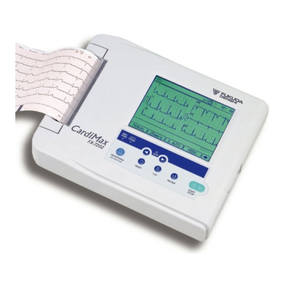
Page 13: Unit (Top Face
Used also to enter patient data or perform various operations by touching the touch-panel keys (soft keys) provided on the screen. (2) Operation panel Provides the controls for the Cardimax FX-7202 operation. (3) Magazine open button Push to open the magazine cover. -
Page 14: Unit (Side, Rear, And Bottom Faces)
Chapter 1 Unit (side, rear, and bottom faces) (7) Potential equalization (6) LAN port (10 BASE T) terminal (9) PATIENT connector (8) AC inlet (11) BATTERY PACK compartment NI-MH BATTERY PACK (10) CARTRIDGE compartment (6) LAN port (10 BASE T) Connect the LAN cable here for connection to a personal computer. -
Page 15: Operation Panel
Press this key to switch the FX-7202 to power ON from standby status. Press this key for 2 seconds or more to switch the FX-7202 from power ON to standby status. Also, press this key for 5 seconds or more to turn OFF the FX-7202 in case there is system trouble. - Page 16 Chapter 1 (6) [1mV] key Press this key to display and record the calibrated 1mV waveform. (7) [RESET] key Press and hold down this key to reset the ECG waveform. The ECG waveform input starts when you release this key. 1 - 4...
-
Page 17: Specifications List
Component Names and Functions Specifications list Lead Standard 12 leads Sensitivity 1/4, 1/2, 1, 2cm/mV, or automatic Polarization voltage ±550mV or greater Frequency response 0.05 to 150Hz Time constant 3.2 sec Common mode rejection 2mmp-p or lower (103dB or more) Input impedance 50M ohms or greater Input circuit current... - Page 18 Chapter 1 1 - 6...
-
Page 19: Maintenance
Chapter Maintenance Cleaning ....................2-1 Cleaning the unit ..............2-1 Replacing the battery................2-2 Installing the optional software............2-4 Self-diagnostics test ................2-5 User self-diagnostics test ............2-6 TEST PATTERN ..............2-7 RECORDING TEST............2-8 KEY TEST................. 2-10 LCD TEST ................ 2-10 BUZZER TEST .............. - Page 20 Checking the patient measurement current ......2-29 Checking the protective earth resistance ......2-30 Inspection of electrical performance/characteristics ....2-31 Hardware inspections (10 items) ...........2-33 Periodical inspection record ............2-35...
-
Page 21: Cleaning
Chapter 2 Maintenance Cleaning ●Cleaning the unit Moisten gauze or absorbent cotton with medicinal alcohol or neutral detergent, and wring tightly; then wipe off the enclosure. CAUTION Prevent chemicals and other liquids from getting inside the unit and connectors. Electrical equipment can short and get damaged. -
Page 22: Replacing The Battery
Chapter 2 Replacing the battery DANGER Before replacing the battery, make sure to turn the power OFF and unplug the power supply cord from the power outlet. 1. Turn OFF the main power switch of the unit and unplug the power supply cord. 2. - Page 23 Maintenance 4. Install a new battery. Insert the battery cable connector to the power supply terminal, and place the battery inside the battery case and mount the battery compartment cover. Battery compartment cover Battery NOTE If the battery compartment cover does not fit well, reinstall the battery and battery cable in the battery case.
-
Page 24: Installing The Optional Software
Chapter 2 Installing the optional software 1. Turn OFF the main power switch of the unit and unplug the power supply cord. 2. Remove the cartridge compartment cover. Remove one screw tightening the cartridge compartment cover on the bottom of the unit. Cartridge compartment Screw cover... -
Page 25: Self-Diagnostics Test
Maintenance Self-diagnostics test The self-diagnostics test function is classified into two types: user self-diagnostics test and manufacturer self-diagnostics test. The user self-diagnostics test is used for a daily check by the user. The manufacturer self-diagnostics test is used for checking and adjusting the unit in a production process or during product inspection, and for the maintenance by the manufacturer. -
Page 26: User Self-Diagnostics Test
Chapter 2 ●User self-diagnostics test Tap the [MENU] key and then tap the [SET UP MODE] key on the [MODE SELECT] screen to go to the [SET UP MODE (MENU)] screen. Tap the [MAINTENANCE] key to go to the [SET UP MODE (MAINTENANCE)] screen that display user self-diagnostics test menus as shown below. -
Page 27: Test Pattern
Maintenance Test Pattern This section explains how to select the built-in electrocardiogram (ECG) test pattern waveform to use during an operation check or demonstration. 1. Tap the [TEST PATTERN] key on the [SET UP MODE (MAINTENANCE)] screen to go to the [MAINTENANCE (TEST PATTERN)] screen. MAINTENANCE (TEST PATTERN) NONE NORMAL... -
Page 28: Recording Test
Chapter 2 Recording Test This section explains how to carry out the recorder test. 1. Tap the [RECORDING TEST] key on the [SET UP MODE (MAINTENANCE)] screen to go to the [MAINTENANCE (RECORDING TEST)] screen shown below. MAINTENANCE (RECORDING TEST) Push 【START/STOP】... - Page 29 Maintenance 4. Tap the [START/STOP] key, then format below will be recorded in the transfer speed of 5mm/sec, 10mm/sec, 12.5mm/sec, 25mm/sec, and 50mm/sec. 20mm 20mm 20mm 20mm The RECORDING TEST in progress is discontinued when the [START/STOP] key is pressed during recording. If the [START/STOP] NOTE key is not tapped, the RECORDING TEST terminates on termination of recording of 50 mm/sec.
-
Page 30: Key Test
Chapter 2 Key test This section explains how to carry out the tests related to key operations. 1. Tap the [KEY TEST] key on the [SET UP MODE (MAINTENANCE)] screen to go to the [MAINTENANCE (KEY TEST)] screen. MAINTENANCE (KEY TEST) Review START STOP... -
Page 31: Buzzer Test
Maintenance BUZZER TEST This test is to check buzzer's tone, etc. 1. Tap the [BUZZER TEST] key on the [SET UP MODE (MAINTENANCE)] screen to go to the [MAINTENANCE (BUZZER TEST)] screen indicated below. MAINTENANCE (BUZZER TEST) MENU EXIT Tapping the "KEY" on the screen produces a buzzer sound. 3. -
Page 32: Manufacturer Self-Diagnostics Test
[SET UP MODE (MAINTENANCE)] screen. Secret number entering procedure is shown below. 1. Tap the [MAKER MAINTENANCE] key on the [SET UP MODE (MAINTENANCE)] screen to go to the [MAINTENANCE (PASSWORD)] screen. MAINTENANCE (PASSWORD) FX-7202 CTL :01-01 NO :00018 Please enter password MENU EXIT 2. - Page 33 Maintenance 4. Processing that corresponds to the entered 4-digit figure is executed when four [numeral] keys are tapped. (See the following correspondence table.) Figure Description of processing ・Turns ON hard copy function. 1024 ・Clears the secret number request message. ・Goes to the [SET UP MODE (MAINTENANCE)] screen. ・Turns OFF hard copy function.
-
Page 34: Status Test
Chapter 2 Status Test This is the test related to the display function for each status of the hardware. 1. Tap the [STATUS TEST] key on the [SET UP MODE (MAKER MAINTENANCE)] screen to go to the [MAINTENANCE (STATUS TEST)] screen. -
Page 35: Lan Test
1. Tap the [LAN TEST] key on the [SET UP MODE (MAKER MAINTENANCE)] screen to go to the [MAINTENANCE (LAN TEST)] screen. 2. Connect the FX-7202 to the host computer with the LAN cable, and set each IP adress of them. -
Page 36: Memory Test
Chapter 2 Memory Test This test is to check read/write from/to the DRAM. 1. Tap the [MEMORY TEST] key on the [SET UP MODE (MAKER MAINTENANCE)] screen to go to the [MAINTENANCE (MEMORY TEST)] screen. 2. Push the [START/STOP] key to start the MEMORY TEST. MAINTENANCE (MEMORY TEST) 0000 0000... -
Page 37: Recorder Test
Maintenance Recorder Test This test is to confirm that the phase adjustment of the thermal print head is correct when moving the recorder. 1. Tap the [RECORDER TEST] key on the [SET UP MODE (MAKER MAINTENANCE)] screen to go to the [MAINTENANCE (RECORDER TEST)] screen. - Page 38 Chapter 2 3. Tap the function key [25mm/s] is suspended to switch the feed rate cyclicly. 25mm/S 50mm/S 5mm/S 10mm/S 12.5mm/S NOTE The feed rate cannot be switched during print-out. 4. By tapping the [MENU] key, the screen returns to the [SET UP MODE (MAKER MAINTENANCE)] screen.
-
Page 39: Touch Panel Test
Maintenance Touch Panel Calibration Touch panel adjustment is performed in this test. 1. Tap the [TOUCH PANEL TEST] key on the [SET UP MODE (MAKER MAINTENANCE)] screen to go to the [MAINTENANCE (TOUCH PANEL TEST)] screen. MAINTENANCE (TOUCH PANEL TEST) Please tap center point MENU RESET... -
Page 40: Internal Memory Initialize
Chapter 2 Internal Memory Initialize The internal memory is initialized by this function. 1. Tap the [INTERNAL MEM. INITIALIZE] key on the [SET UP MODE (MAKER MAINTENANCE)] screen to go to the [MAINTENANCE (INTERNAL MEM. INITIALIZE)] screen. MAINTENANCE (INTERNAL MEM. INITIALIZE) Do you initialize internal memory ? MENU RESET... -
Page 41: Fx7202 Update
Maintenance FX7202 UPDATE Update the software incorporated in the Electrocardiograph. 1. Transition to the following [MAINTENANCE (FX7202 UPDATE)] screen occurs when the [FX7202 UPDATE] key is tapped in the [SET UP MODE (MAKER MAINTENANCE)] screen. MAINTENANCE (FX7402 UPDATE) Update Start HOST MENU RESET... -
Page 42: Periodical Inspections
Chapter 2 Periodical inspections To maintain the unit's functions and performance, periodical inspections are required. The inspections explained in this section should be performed by service representatives who have sufficient technical knowledge. ●Periodical inspection intervals and precautions Inspection item Description Periodical inspection interval Periodical inspection should be performed at least once a year. -
Page 43: Safety Inspections (6 Items)
Maintenance ● Safety inspections (6 items) Safety-related testing methods and measurement equipment are prescribed in safety test standards. At the actual sites where medical treatment is being given, however, it can be extremely difficult to verify that everything meets the standards. For this reason, when performing inspections, set up and make acceptance determinations using the methods described below. - Page 44 Chapter 2 Electric current calculation method When checking a leakage current, measure the AC voltage by using a leakage current measuring device (MD). Convert the measured voltage to current by employing the formula below. If the phase is switched and measurements are made, use the higher voltage to calculate the current.
-
Page 45: Checking The Earth Leakage Current (Current That Flows To Protective Earth Resistance)
Checking the earth leakage current (current that flows to protective earth resistance) Measurement wiring diagram Conversion plug Used for single fault condition Power outlet Conversion plug FX-7202 FX-4010 Power supply cord Power cable Measurement Measurement point A point B Leakage current measuring device... -
Page 46: Checking The Enclosure Leakage Current
Checking the enclosure leakage current (current that flows from the enclosure to the earth terminal of the power outlet) Measurement wiring diagram This terminal is open. Conversion plug Power outlet Used for single fault condition FX-7202 FX-4010 Power supply Power cable cord Measurement Measurement point A... -
Page 47: Checking The Patient Leakage Current I
Maintenance Checking the patient leakage current I Measurement wiring diagram This terminal is open. Conversion plug Power outlet Used for single fault condition FX-7202 FX-4010 Power supply cord Power cable Measurement Measurement point A Short all electrodes. point B Leakage current... -
Page 49: Checking The Patient Measurement Current
Maintenance Checking the patient measurement current Measurement wiring diagram This terminal is open. Conversion plug Power outlet Used for single fault condition FX-7202 FX-4010 Power supply cord Power cable Measurement Measurement point B point A Leakage current measuring device Patient measurement current measurement points... - Page 52 Chapter 2 5.Counter electrode voltage Check that the change in the recorded sensitivity is within ±5% when ±550 mV of DC voltage is imposed to the input of the Electrocardiograph. Check that the change in the recorded sensitivity is within ±5% when ±550 mV of DC voltage is imposed between the two input terminals of the Electrocardiograph and the RF(N) electrode fitting.
-
Page 53: Hardware Inspections (10 Items)
Maintenance ●Hardware inspections (10 items) WARNING If, during a hardware inspection, you notice damage or other abnormality, immediately stop using the given unit; then replace the defective part, replenish, or make proper repairs. Failure to repair the unit can lead to a serious accident. Do not replace the part nor carry out refilling or the like but change the hardware (MAIN BOARD, for ex.) found faulty. - Page 54 Chapter 2 Checking the switches Description Check for unsmooth operation, damage, and rattling. Checking the recorder Description Check that recording operation is smoothly performed and no abnormal noise exists. Checking the electrodes Description Check the electrodes for corrosion, and their chip-mounting area for wear, safety defects, malfunctional operation, and damage.
-
Page 55: Periodical Inspection Record
Maintenance Periodical inspection record Remarks Procedure/measurement value Judge- Item Description (Repair Acceptance standard ment required 1. Power supply cord, patient cable, etc. Any flaws or damages? OK・NG Cables 2. Limb electrode, chest electrode, etc. Any contamination or rust adhered? OK・NG Electrodes 3. - Page 56 Chapter 2 Remarks (Acceptance Measurement Judge-men Description (Repair standard) value required 1. Earth leakage Normal condition OK・NG (0.5mA or less) current Single fault condition (1.0mA or less) OK・NG 2. Enclosure leakage Normal condition (0.1m or less) OK・NG current Single fault condition (0.5mA or less)...
-
Page 57: Disassembly
Chapter Disassembly Removing the enclosure cover ............3-1 Removing the main board ..............3-2 Removing the recorder unit ............... 3-3 Removing the ECG AMP unit ............. 3-4... -
Page 59: Removing The Enclosure Cover
Chapter 3 Disassembly Removing the enclosure cover 1. Remove the 4 mounting screws (seven). Mounting screws 2. Remove the enclosure cover. Enclosure cover 3 - 1... -
Page 60: Removing The Main Board
Chapter 3 Removing the main board CAUTION To prevent damage by static electricity, eliminate static electricity from your body before touching the board. 1. Remove the enclosure cover. For details on removing procedures, see page 3-1, "Removing the enclosure cover." 2. -
Page 61: Removing The Recorder Unit
Disassembly Removing the recorder unit 1. Remove the enclosure cover. For details on removing procedures, see page 3-1, "Removing the enclosure cover." 2. Remove the connectors (P6 and P9) connected to the MAIN BOARD. 3. Remove the mounting screws (three) to remove the recorder unit. Recorder unit Mounting screw 3 - 3... -
Page 62: Removing The Ecg Amp Unit
Chapter 3 Removing the ECG AMP unit CAUTION To prevent damage by static electricity, eliminate static electricity from your body before touching the board. 1. Remove the enclosure cover and the main board. For details on removing procedures, see page 3-1, "Removing the enclosure cover"... -
Page 63: Electric Circuit Diagrams
Clock generator section ............ 4-12 ECG AMP BOARD block diagram......... 4-13 OPERATION BOARD block diagram ........4-15 POWER BOARD block diagram ........... 4-16 FX-7202/FCP-7201 Block Diagram ........... 4-17 MAIN BOARD Circuit Diagrams (PCB-6868) ........4-18 Power DC/DC converter block ..........4-18 CLK block................4-19 MAIN CPU block .............. - Page 64 POWER LED block ...............4-31 ECG AMP BOARD Circuit Diagrams (PCB-6867A) ......4-32 AMP block ................4-32 LAN PORT block ..............4-33 Bypass condenser block ............4-34 OPERATION BOARD (PCB-6866C)...........4-35 Touch panel/LCD/KEY I/F............4-35 Back light block ..............4-36 MAIN POWER SUPPLY..............4-37 CHARGE.....................4-38 LOGIC 1 ....................4-39 LOGIC 2 ....................4-40 MAGAZIN SW BOARD...............4-41 MARK SENSER BOARD..............4-42...
-
Page 65: Overall Block Diagram Of Unit
Electric Circuit Diagrams Overall block diagram of unit The FX-7202 circuitry can roughly be divided into 5 functions below. 1.MAIN BOARD(PCB-6868) 2.ECG AMP BOARD(PCB-6867) 3.OPERATION BOARD(PCB-6866) 4.POWER BOARD(PCB-6863) 6.CARTRIDGE BOARD(PCB-6818) [option] The electrocardiographic signal input through the patient connector is boosted and is... -
Page 66: Main Board Block Diagram
Chapter 4 ●MAIN BOARD block diagram The following shows a block diagram of the MAIN BOARD. * Thick line represents a bus, and dotted line a reset signal. CARTRIDGE BOARD FLASH ROM MAIN CPU (SH7709A) (128MHz) MAIN G/A RESET SDRAM 16MB MOTOR DRIVER... -
Page 67: Main Cpu Section
Electric Circuit Diagrams MAIN CPU section The MAIN CPU, which uses SH7709A, carries out processing of electrocardiogram display, record, other basic operations as electrocardiograph, processing of LAN, supervision of backup battery, and processing related to mark sensor. The internal clock which operates at 128 MHz controls the address bus, data bus, peripheral devices, and performs different actions according to setting determined by software. -
Page 68: Memory Section
Chapter 4 Memory section The memory section can be divided into the following blocks. (1) FLASH ROM (2) SDRAM (1) FLASH ROM The FLASH ROM, which used one E28F640J3A-120 (64Mbit), is used for program store, function setting store, electrocardiogram data store, etc. - Page 69 Electric Circuit Diagrams (2) SDRAM Consisting of two MT48LC8M16A2TG-75's (128 Mbits), the SDRAM is used for program store and waveform work area. 4 - 5...
-
Page 70: Amp, Lan Interface Section
Chapter 4 AMP, LAN interface section [B100kHz] and [B100kHz_L] are square waves for driving the transformer of pulses output from the MAIN G/A. To the line of send/receive data ([TXD]/[RXD]) from the ECG AMP BOARD, diodes (D4, 5) are connected for protection from electrostatic charge or other excessive voltages. -
Page 71: Lcd Controller Section
Electric Circuit Diagrams LCD controller section As a device, S1D13705 is used. Thermal head control section The thermal head signal from the MAIN G/A is output to the thermal head. To each signal line, a buffer for level change and an R and L network as a filter are connected. -
Page 72: Motor Control Section
Chapter 4 Motor control section The MTD2007F (IC29) is equipped as a motor control IC to control the stepping motor of the recorder block. Real time clock As a real time clock device, RTC-4574SAA incorporating a crystal resonator of 32.768 kHz is used. The real time clock is driven by [VBAT]. Therefore, unless the Ni-MH battery (BT1) is mounted, the real time clock does not work. -
Page 73: Wait Control Section
Electric Circuit Diagrams Wait control section In the wait control section, GAL16LV8C-15J of CMOS PLD is used. This device processes a wait signal output from the MAIN G/A, LCD controller or other control ICs, and outputs an optimum wait signal to the MAIN CPU. -
Page 74: Sensor Control Section
Chapter 4 Sensor control section There are magazine UP sensor and mark sensor. As for the magazine UP sensor, a signal is output through connector P7 pin 1. Opening the magazine turns off the switch and transmits "L" level signal to the MAIN CPU. -
Page 75: Operation Interface And Power Interface Section
Electric Circuit Diagrams OPERATION interface and power interface section The OPERATION interface section transfers to the OPERATION BOARD the data from the LCD controller, control signals from the POWER BOARD and different supply voltages. The power interface section transfers to the OPERATION BOARD control signals from the POWER BOARD. -
Page 76: Power Generator Section
Chapter 4 Power generator section Inputting +5 V to DC-DC converter generates the MAIN CPU core voltage +1.9 V. Output voltage VOUT is set by the following expression according to R51, R52 and R53. VOUT=0.8(1+R51/(R52+R53)) Clock generator section The clock generator section generates clock frequencies necessary for the MAIN CPU, MAIN G/A and other control ICs. -
Page 77: Ecg Amp Board Block Diagram
Electric Circuit Diagrams ●ECG AMP BOARD block diagram The following shows a block diagram of the ECG AMP BOARD. 20Bit ⊿ΣADC Photcoupler 20bit ADC 20bit ADC Control GA 20bit ADC 20bit ADC 20bit ADC +5VD 20bit ADC Isolation Power +5VA 20bit ADC 100KHz 20bit ADC... - Page 78 Chapter 4 The RJ-45 connector provided allows the instrument to be easily connected to a LAN system using twisted pair cable. Since all the signals are isolated with the pulse transformer, it is not required to separately provide an external isolation system. 4 - 14...
-
Page 79: Operation Board Block Diagram
Electric Circuit Diagrams ●OPERATION BOARD block diagram The following shows a block diagram of the OPERATION BOARD. POWER POWER CHARGE BAT. LED BATTERR ON/OFF ON/OFF KEY MAIN BOARD KEY-SCAN KEY-DATA 3x3 KEY Matrix +15V TCP-SEL Touch Panel Driver TOUCH PANEL AD-DATA MAIN ADS7816... -
Page 80: Power Board Block Diagram
Chapter 4 ●POWER BOARD block diagram This board supplies and controls voltages delivered to each circuit board. It generates +3.3 V, +5 V, +15 V and +24 V. The following shows a block diagram of the POWER BOARD. AC90~264V 47~53Hz TRANS THERMAL HEAD... - Page 81 FX-7202 Block Diagram Battery pack LOWER CASE UPPER CASE AC inlet FFC cable OPERATION BOARD POWER SUPPLY FFC cable UNIT AIN BOARD FFC cable Thermal head Operation key input cable cable icro swich JTAG Photo sensor Sepping mortor FFC cable...
-
Page 82: Main Board Circuit Diagrams (Pcb-6868B)
MAIN BOARD Circuit Diagrams (PCB-6868B) ● Power DC/DC converter block +1.9V LQN6C4R7M04 4.7uH 0.051J(1W NPR) SI3443DV +1.9VPOWER SUPPLY 91KF LTC1622CMS8 CP454 CP455 SENSE PDRV 330UF/6.3V(O) RUN/SS SYNC/MODE 10KF 33KF 0.1uFFZ D3FS4A 0.1uFFZ 100UF/10V(C)5 220pFCHJ 470pFCHJ 33KF 220pFCHJ IC4A CP456 HD74ACT244 IC28A IC28B ( 4,13 ) -
Page 83: Clk Block
●CLK block +3.3V CP12 4.7UF/6.3V(T)3 16MHz LCDCCLK2 ( 13 ) 0.01uFBJ 0.01uFBJ +3.3V MG-5100SA-FD VDD1 CP13 VDD2 CP14 CP15 16MHz CLKA TCLK ( 3 ) CLKB 7.3728M ( 4 ) 20MHz CLKC 20M_LAN ( 11 ) CLKD R278 10KF CPUCLK XBUF CP16 32MHz... -
Page 84: Main Cpu Block
●MAIN CPU block MA[0..25] MA[0..25] ( 7 ) +1.9V MD[0..31] MD[0..31] ( 6,7,11 ) 0.1uFFZ CP441 470pFCHJ +1.9V CP129 CP127 0.1uFFZ CP128 ( 2 ) TCLK ( 2 ) MCPUCLK MWR0_1_L ( 4,13 ) 0.1uFFZ CP22 CP23 MWR0_2_L ( 6 ) 10KF CP442 CP132... -
Page 85: Main Ga Block
●MAIN GA block +3.3V RM10 EXBD10C103J RM11 EXBD10C103J MDD[0..31] ( 7,13 ) MDD[0..31] MAA[0..25] ( 7,13 ) MAA[0..25] 0.1uFFZ 0.1uFFZ FD00027-MC 1.0UF/16V(T)3 1.0UF/16V(T)3 1.0UF/16V(T)3 1.0UF/16V(T)3 ( 3,13 ) MRD_1_L MRD* FMBA0 ( 3,13 ) MWR0_1_L MWR0* FMBA1 ( 3,13 ) MWR1_1_L MWR1* FMCS*... -
Page 86: From Block
●FROM block MDE[0..15] ( 6 ) MDE[0..15] MAB[0..25] ( 6,7,11 ) MAB[0..25] F ROM U 32M/64M/128M Intel Strate Frash MD[0..31] ( 3,7,11 ) MD[0..31] MDE0 MAB1 MDE1 MDE0 MAB2 MDE2 MDE1 MAB3 MDE3 MDE2 MAB4 MDE4 MDE3 MAB5 MDE5 MDE4 MAB6 MDE6 MDE5... -
Page 87: Sdram Block
●SDRAM reset block MDE[0..15] ( 5 ) MDE[0..15] MAB[0..25] +3.3V ( 3,7,11 ) MAB[0..25] CP223 CP224 64M/128M MAB1 CP225 MDE0 MAB2 CP226 MDE1 JP12 MAB13 MAB3 CP227 MDE2 0.1uFFZ CP241 MAB4 CP228 MDE3 10UF/6.3V(T)3 JP13 0.1uFFZ MAB14 MAB5 CP229 MDE4 VBAT ( 7 ) MAB6... -
Page 88: Rtc/Main Wait Block
●RTC/MAIN WAIT block MA[0..25] MAA[0..25] MA[0..25] MAA[0..25] CP242 ( 3 ) ( 4,13 ) CP243 MD[0..31] MDD[0..31] ( 3,5,11 ) MD[0..31] MDD[0..31] CP244 MAA0 CP293 ( 4,13 ) CP245 MAA1 CP294 CP246 MAA2 CP295 R130 MDD0 CP247 MAA3 R131 CP296 MDD1 CP248 MAA4... -
Page 89: Power I/F Block
●POWER I/F block +3.3VSTB ( 12 ) POWER_ON R163 BATT_VOL 100F +3.3VA 1SS302 R164 BATT_TMP 100F +3.3VA +3.3V 1SS302 IC7G HD74LVC244A BATT_STS (+3.3V) AC_FAIL_L AC_DETECT POWER UNIT I/F CN (SIGNAL) IC7F HD74LVC244A CP331 +3.3V AC_LED (+3.3V) R168 +3.3V IC13A CP332 HD74LVC04 CP333 ( 3,13 ) -
Page 90: Amp Thermal Block
●AMP THERMAL block FROM AMP RXD-A ( 11 ) TXD-A ( 11 ) R171 100KF +3.3V CP346 IC15A IC14B + 3 . 3 V S D A 1SS302 ( 4 ) RXDA S C L R E S E T TC7W14FU TC7W14FU ( N C ) -
Page 91: Senser/Buzzer/Motor Drv Jtag I/F Block
●SENSE/BUZZER/MOTOR DRV JTAG I/F block ( 4 ) HEADUP_L +3.3VA +3.3V R188 R189 +3.3V 510F 10KF IC17B 0.1uFFZ IC17A MAX4163EUA MAX4163EUA 1SS302 ( 3 ) MARK_V R194 0.1uFFZ 100F CP462 470pFCHJ FOR RECORDER 1SS302 R192 R190 CP355 100KF 100F +3.3V R193 R191 100KF... -
Page 92: Lan Port/Amp I/F Block
●LAN PORT/AMP I/F block NFM2012P13C474F +3.3V CP358 +3.3V 0.1uFFZ 0.1uFFZ 4.7UF/6.3V(T)3 0.1uFFZ 0.01uFFZ 0.1uFFZ 0.01uFFZ 0.01uFFZ 0.1uFFZ 4.7UF/6.3V(T)3 MAB[0..25] ( 5,6,7 ) MAB[0..25] IC18 MD[0..31] LAN91C96 ( 3,6,7 ) MD[0..31] MAB0 CP382 CP392 TPERXP MAB1 CP383 CP393 61.9F TPERXN R223 MAB2 CP384 CP394... -
Page 93: Key/Lcd I/F Block
●KEY/LCD I/F block +3.3V IC7D R235 100F ( 3,13 ) POWER_KEY HD74LVC244A CP396 100F R234 ( 13 ) KEY_RESET_L +3.3VSTB +3.3VSTB 1SS302 +3.3VSTB IC20B 100F R236 CP465 CP466 ( 8 ) POWER_ON IC21C IC21A R240 R264 TC7W14FU TC7W14FU 10KF R241 0.1uFFZ 10KF TC7W74FU... -
Page 94: Lcd Control Block
●LCD controler block MAA[0..25] MDD[0..31] ( 4,7 ) MAA[0..25] MDD[0..31] ( 4,7 ) IC23 MAA0 MAA1 MDD0 MAA2 MDD1 MAA3 MDD2 MAA4 MDD3 MAA5 MDD4 MAA6 MDD5 MAA7 MDD6 +3.3V MAA8 MDD7 MAA9 MDD8 MAA10 MDD9 AB10 MAA11 MDD10 AB11 DB10 MAA12 MDD11... -
Page 95: Power Led Block
●POWER LED block +3.3V C211 C128 C129 C130 C131 C132 C133 C134 C135 C136 C137 C207 0.1uFFZ +1.9V POWER UNIT I/F CN (POWER) 0.1uFFZ 0.1uFFZ 0.1uFFZ 0.1uFFZ 0.1uFFZ 0.1uFFZ 0.1uFFZ 0.1uFFZ 0.1uFFZ 0.1uFFZ 0.1uFFZ +3.3V +3.3V C106 100UF/10V(C)5 C109 C110 C111 C138 C139... -
Page 96: Ecg Amp Board Circuit Diagrams (Pcb-6867A)
ECG AMP BOARD Circuit Diagrams (PCB-6867A) ● AMP block IC2A E25F ADS1252U TLC2264C C2-F TC-74VHC00FT 10KF 300F VIN+ DOUT3 IC14A IC15 +5VF 24KF 130F VIN- DOUT VREF 24KB SCLK 300MM 150P VREF 300F 10KF 0.22uF 0.1uF FMW2 E25F 69.8KB E25F IC2B TC-74VHC00FT 10KF... -
Page 97: Lan Port Block
●LAN PORT block LAN PORT TXD(+) TXD(-) RXD(+) RXD(-) TRANSMIT PE-64681 FRAME 10FMN-BMTTR-A-TB TM11R-5C-88 TXD-A ( 1 ) RXD-A ( 1 ) RECEIVE B100kHz ( 1 ) B100kHz_L ( 1 ) PE-65421 3Y06-230P1 0.01uFFZ 0.01uFFZ 4 - 33... -
Page 98: Bypass Condenser Block
●Bypass condenser block AMP block bypass capacitor AMP部パスコン +5VF +5VF FD00026-AC HCPL2601 TC-74VHC00FT TC-74VHC164FT +2.5VF +2.5VF -2.5VF 10/10V 10/10V 10/10V 10/10V AGND ADS1251U -2.5VF VREF 3.3/10V 3.3/10V 3.3/10V 3.3/10V 3.3/10V ADS1251U -2.5VF +2.5VF +2.5VF E25F -2.5VF TLC2264C TLC2252C OPA2350EA -2.5VF HCPL2601 4 - 34... -
Page 99: Touch Panel/Lcd/Key I
OPERATION BOARD (PCB-6866C) ●Touch panel/LCD/KEY I/F POWER SKRAAAE010 LED1B NSCB100 POWER LED2B NSCB100 CHARAGE LED3B SML-012YT BATT_ERR SKRAAAE010 SKRAAAE010 SKRAAAE010 REVIEW > LEAD RESET < LEAD START/STOP SKRAAAE010 SKRAAAE010 SKRAAAE010 SPARE 1 SPARE 2 SPARE 3 SKRAAAE010 SKRAAAE010 SKRAAAE010 10KF CP12 1SS302 1SS302 1SS302 1SS302... -
Page 100: Back Light Block
●Back light block CP34 CP35 +15V LQH32CN100K21 +28V CRS01 121KF 100KF CP37 CP36 220UF/50V(C) SHDN UNMOUNT 1.0UF/50V(C)7 4.7KF 220UF/25V(C) LT1930ES5 4.7UF/25V(C)7 1000PF +28V 100KF 100KF IC10B CP41 CP43 IC10A CP39 UPC358G2 CP40 LCD_CONT 2SC3736 100F 100KF LCD_POWER ( 1 ) UPC358G2 CP38 CP42... -
Page 101: Main Power Supply
MAIN POWER SUPPLY NC-187-10N DF13-15P-1.25V(20) 2SC2873-Y 2SJ529S TR5-T ELF25C 250Vac ELF18D 275Vac 2.5A 012A 470p 0.22u 417F 1W [0.047] 〜 +24V 275Vac 2.2K 630V 0~1.3A TR5-T 0.22u 2.5A CR73 〜 D3FS4A 1SS184 250Vac 470p 275Vac uPC339G2 0.22u U71A U71C AC90~264V :47~63Hz JTR-02B 4.7K 470K... -
Page 102: Charge
CHARGE 6P-SCN VBAT(+) 451015 BATSNS VBAT(-) R132 R133 Q138 CR134 0.1W 1K 0.1W 2.7K uPA1730G CR132 L131 L132 1SS184 CR136 Q131 Q133 RD15MB2 CR135 DF10SC4M 2SC2873-Y uPA1730G VCHG(+) R134 Q132 1.5K DE5LC20U 2SJ529S R135 C142 C141 4.7K 0.01u 1000P CR137 1SS184 VCHG(-) R137... -
Page 103: Logic 1
LOGIC 1 00-6208-520-020-000 ACLED AC_LED BATT_VOL BATVOL BATT_TMP BATTMP 3.3STB +3.3V STB CR204B 1SS272 S-873325BUP-ALA Q202 Q200 R201 DTA114EUA 2SC2873-Y 24VSUP U200 Q201 R200 2SC2712-Y VBAT(+) 100K Q203 DTC114EUA E1(DG) E1(DG) 3.3RESET E1(DG) 3.3STB U205 C220 TC74VHC132FT Q204 VBATGOOD 630V 0.01u R202 R203 U202... -
Page 104: Logic 2
LOGIC 2 3.3V 24VSUP 5VSTB VBAT(+) 24VSUP 20VSUB VTEMP CR300A ≧ ACDET 14.4V uPC339G2 1SS184 U304 U303 CR300B 1SS184 U304 uPC324G2 ≧ ℃ uPC324G2 U303 ≦ R327 S-80940CNNB-G9A C316 uPC339G2 U303 0.01u 4.7K BATDET U300 uPC339G2 U301 TA78L05F U304 CR304A VBATOP 1SS272 uPC324G2... -
Page 105: Magazin Sw Board
Electric Circuit Diagrams MAGAZIN SW BOARD DF4-2P-2C FRAME FRAME ESE11SH2C 4 - 41... -
Page 106: Mark Senser Board
Chapter 4 MARK SENSER BOARD MARK-COM MARK-E Recording MARK-A DF4-3P-2C paper CN2253 4 - 42... -
Page 107: Spare Parts List
Chapter Spare Parts List MAIN BOARD (PCB-6868B) ..............5-1 ECG AMP BOARD (PCB-6867A)............5-5 OPERATION BOARD (PCB-6866C) ............ 5-7 POWER1 BOARD (PCB-6863B)............5-9 POWER2 BOARD (PCB-6864B)............5-13 MARK SENSER BOARD (PCB-6865) ..........5-14 MAGAZIN SW BOARD (PCB-6862) ..........5-14... -
Page 109: Main Board (Pcb-6868B)
Chapter 5 Spare Parts List MAIN BOARD (PCB-6868B) Config. No. Part name Specification Q'ty Battery CR-2032 (BT) (1) Battery case BCR20H5 Buzzer PKM13EPY-4002 Chip laminate ceramic GRM39CH221J50 capacitor Chip laminate ceramic GRM39CH471J50 capacitor 106 107 Chip electrolytic UUT1A101MCR1GS capacitor Chip laminate ceramic GRM39F104Z25 capacitor Surface mnunt type... - Page 110 Chapter 5 214 215 218 219 Chip laminate ceramic GRM21B2C1H102AJ capacitor Chip type aluminum MVY35VC100MH10 electrolytic capacitor 224 225 Chip type aluminum UUD1V680MCR1GS electrolytic capacitor Schottkey barrier D3FS4A diode Switching diode 1SS302 HD6417709AF133 G. A FD00027-MC DC/DC controller LTC1622CMS8 Logic IC HD74ACT244TTP-20DA Zero Delay Buffer CY2305SC-1...
- Page 111 Spare Parts List Connector 18-5085-006-000-808 Connector DF13B-9P-1.25V(21) P-chanel MOS FET SI3443DV Digital transistor UN2212 Silicon transistor 2SC2712 Digital transistor DTC124EUA Digital transistor UN5212 RK73H1J TD 10 K Ω F Square chip resistor 0.051 Ω J Square chip resistor NPR1 RK73H1J TD 91 K Ω F Square chip resistor RK73H1J TD 33 K Ω...
- Page 112 Chapter 5 264 295 RK73H1J TD 15 K Ω F Square chip resistor 265 296 Ω F Square chip resistor RK73H1J TD 7.15K 266 297 RK73H1J TD 4.12 K Ω F Square chip resistor 171 192 193 RK73H1J TD 100 K Ω F Square chip resistor 178 181 RK73H1J TD 20 K Ω...
-
Page 113: Ecg Amp Board(Pcb-6867A)
Spare Parts List ECG AMP BOARD (PCB-6867A) Config. No. Part name Specification Q'ty Chip laminate ceramic GRM39F104Z25 capacitor Chip laminate ceramic GRM39CH151J50 capacitor Chip laminate ceramic GRM39B561K50 capacitor Chip laminate ceramic GRM39CH330J50 capacitor Chip laminate ceramic GRM39F224Z25 capacitor Tantalum capacitor ECST0GY 226 Chip OS capacitor 16SVP15M... - Page 114 Chapter 5 Assembled transistor FMW2 Transistor 2SK2112 RK73H1J TD 24 K Ω F Square chip resistor Square chip resistor RN73F2A TD 24 K Ω B RK73H1J TD 10 K Ω F Square chip resistor Square chip resistor RK73H1J TD 10 K Ω F Square chip resistor TSR6GTM-307V 300M Ω...
-
Page 115: Operation Board (Pcb-6866C)
Spare Parts List OPERATION BOARD (PCB-6866C) Config. No. Part name Specification Q'ty Chip laminate ceramic GRM39F103Z50 capacitor Chip laminate ceramic GRM39F104Z25 capacitor Chip type aluminum UUD1E221MNR1GS electrolytic capacitor Smoothing ceramic C3225JB1E475K capacitor Smoothing ceramic C3225JB1H105K capacitor Aluminum electrolytic UUD1H221MNR1GS capacitor Chip type aluminum 35CV47AX electrolytic capacitor... - Page 116 Chapter 5 2SJ179 RK73H1J TD 3.0 K Ω F Square chip resistor RK73H1J TD 10 K Ω F Square chip resistor RK73H1J TD 1.0 K Ω F Square chip resistor Square chip resistor RK73H1J TD 121 K Ω F Square chip resistor RK73H1J TD 49.9 K Ω...
-
Page 117: Power1 Board (Pcb-6863B)
Spare Parts List POWER1 BOARD (PCB-6863B) Config. No. Part name Specification Q'ty Capacitor ECQU2A105ML Capacitor DE1B3KX471KA5B Capacitor DE1E3KX102MA5BA01 Capacitor ECQU2A224ML Capacitor GRM55XB32J224K Capacitor GRM31CR72E473K Capacitor CF42W5R471M2000A Capacitor MVE35V100MF80 24-A Capacitor KME25VB220M Capacitor MVY25VC470MJ10 Capacitor Open Capacitor GJ232RF11H475ZD01 170 171 Capacitor GRM31A5C2J471J Capacitor GRM32RB11H105K... - Page 118 Chapter 5 CR 53 Diode DF10SC4M CR 72 Diode RD15MB2 CR 73 112 Diode D3FS4A CR 74 203 204 Diode 1SS272 CR 75 Diode RD12MB2 CR 123 USF8G48 CR 131 Diode DE5LC40 CR 135 Diode DE5LC20U CR 138 Diode RD8.2MB2 CR 200 Diode RB400D...
- Page 119 Spare Parts List Resistor RK73H1JTD 10K F 140 Resistor RK73K1JTD 47K J Resistor RK73K1JTD 220K J 122 123 Resistor RK73Z1J TD 0 J 201 354 Resistor RK73K1JTD 100 J Resistor SL1TE 5m F Resistor RK73H1JTD 150K F Resistor RK73H1JTD 33K F Resistor RK73H1JTD 3.3K F Resistor...
- Page 120 Chapter 5 Resistor RK73H1JTD 22K F Resistor RK73H1JTD 39K F Resistor RK73K1JTD 200K J Open (1608) Transformer JTR-02B Photo coupler TLP621F(D4-GR-LF2) MAX668EUB UPC339G2 UPC1251G2 LM2672M-ADJ LM2672M-5.0 LM2672M-3.3 131 300 TA78L05F bq2004ESN S-873325BUP-ALA-T2 TLC393ID TC74LCX240FT TC74LCX02FT TC7W74FU TC74VHC132FT TC74LCX244FT S-80940CNNB-GQA UPC1093T UPC324G2 TC74VHCT00AFT TC74VHC02FT...
-
Page 121: Power2 Board (Pcb-6864B)
Spare Parts List POWER2 BOARD (PCB-6864B) Config. No. Part name Specification Q'ty Chip capacitor GRM31MB11H224K Chip capacitor GRM188R11H102K Chip capacitor GRM32NF11E106Z Chip capacitor GRM21BR11H104K Chip capacitor GRM1882C1H271J Chip capacitor GRM188R11H103K Chip capacitor GRM31MF11E105K Chip capacitor GRM21BR11E474K Chip capacitor GRM188B11H222K Chip capacitor GJ232RF11H475ZD01 Chip capacitor GRM188F11A105Z... -
Page 122: Mark Senser Board (Pcb6865)
Chapter 5 MARK SENSER BOARD (PCB-6865) Config. No. Part name Specification Q'ty Reflecting photo ON2253 sensor Cable T024407 Pretreated substrate T023405 1/50 Customer control number: PCB-6865 (50/sheet circuit board) Circuit diagram T024123 MAGAZIN SW BOARD (PCB-6862) Config. No. Part name Specification Q'ty Earth detect switch... -
Page 123: Board Component Diagram
Chapter Board Component Diagram MAIN BOARD (PCB-6868B component side)........6-1 MAIN BOARD (PCB-6868B soldering side) ........6-2 ECG AMP BOARD (PCB-6867A component side)......6-3 ECG AMP BOARD (PCB-6867A soldering side)........ 6-4 OPERATION BOARD (PCB-6866C component side) ......6-5 OPERATION BOARD (PCB-6866C soldering side) ......6-6 POWER1 BOARD (PCB-6863B component side) ...... -
Page 125: Main Board (Pcb-6868B Component Side)
MAIN BOARD (PCB-6868B component side) 6 - 1... -
Page 126: Main Board (Pcb-6868B Soldering Side)
MAIN BOARD (PCB-6868B soldering side) 6 - 2... -
Page 127: Ecg Amp Board (Pcb-6867A Component Side)
ECG AMP BOARD (PCB-6867A component side) 6 - 3... -
Page 128: Ecg Amp Board (Pcb-6867A Soldering Side)
ECG AMP BOARD (PCB-6867A soldering side) 6 - 4... -
Page 129: Operation Board (Pcb-6866C Component Side)
OPERATION BOARD (PCB-6866C component side) 6 - 5... -
Page 130: Operation Board (Pcb-6866C Soldering Side)
OPERATION BOARD (PCB-6866C soldering side) 6 - 6... -
Page 131: Power1 Board (Pcb-6863B Component Side)
POWER1 BOARD (PCB-6863B component side) 6 - 7... -
Page 132: Power1 Board (Pcb-6863B Soldering Side)
POWER1 BOARD (PCB-6863B soldering side) 6 - 8... -
Page 133: Power2 Board (Pcb-6864B Component Side)
POWER2 BOARD (PCB-6864B component side) 6 - 9... -
Page 134: Power2 Board (Pcb-6864B Soldering Side)
POWER2 BOARD (PCB-6864B soldering side) 6 - 10... -
Page 135: Mark Senser Board (Pcb-6865 Component Side)
MARK SENSER BOARD (PCB-6865 component side) 6 - 11... -
Page 136: Magazin Board (Pcb-6862 Component Side)
MAGAZIN SW BOARD (PCB-6862 component side) 6 - 12... -
Page 137: Assembly Diagrams
Chapter Assembly Diagrams Recorder 1/4 ..................7-1 Recorder 2/4 ..................7-2 Recorder 3/4 ..................7-3 Recorder 4/4 ..................7-4 External view of recorder ..............7-5 LCD module ..................7-6 Upper case................... 7-7 ECG Amp ..................... 7-8 Main Board................... 7-9 Power supply unit ................7-10 Lower case .................. -
Page 139: Recorder 1/4
Recorder 1/4 2-W sems M2.6x6 2-W sems M2.6x6 2-E ring, nominal :3 2-W sems M2.6x8 2-E ring, nominal :4 Part No. Drawing No. Name and type Q’ty Remarks Magazine base Push button (SU) Button spring Hook mounting shaft Paper support SU Hock Platen rall Bearing DDL-1150ZZ... -
Page 140: Recorder 2/4
Recorder 2/4 E ring, nominal :2.5 2-W sems M2.6x6 2-W sems (L) M3x8 E ring, nominal :2 2-W sems M3x6 2-Polyethylene slider STW6.0-0.25 2-W sems M2.6x5 Part No. Drawing No. Name and type Q’ty Remarks Recorder base SU Platen roll guide plate SU Adjust screw Gasket UC300284V0 Thermal head fixing collar... -
Page 141: Recorder 3/4
Recorder 3/4 W sems M2.6x6 2-W sems M2.6x5 Part No. Drawing No. Name and type Q’ty Remarks Paper case SU Hook bearing stand (A) SU Magazine UP substrate Hook bearing stand (B) Mark sensor substrate Paper guide Brass spacer BSB-2607 7- 3... -
Page 142: Recorder 4/4
Recorder 4/4 2-flat head M3x6 2-W sems M2.6x6 2-E ring, nominal :3 Part No. Drawing No. Name and type Q’ty Remarks Recorder unit assembly diagram (1) Recorder unit assembly diagram (2) Recorder unit assembly diagram (3) Magazin mounting shaft Paper cutter 7 - 4... -
Page 143: External View Of Recorder
External view of recorder 7- 5... -
Page 144: Lcd Module
LCD module 4-double-faced adhesive tape 4-W sems M3x6 Part No. Drawing No. Name and type Q’ty Remarks 9H6494 Touch panel LCD mounting plate 7 - 6... -
Page 145: Upper Case
Upper case View from A 4-W sems M3x6 Part No. Drawing No. Name and type Q’ty Remarks Top cabinet 2-W sems M3x10 2-W sems M3x6 Switch sheet Si packing, large Si packing, small Substrate power supply CE Mark nameplate Operation panel substrate assembly LCD module assembly 7- 7... -
Page 146: Ecg Amp
ECG Amp 2-W sems M3x8 W sems M3x6 2-W sems M3x14 Adhere double-faced adhesive tape to rear surface. 2-W sems M3x4 2-W sems M3x4 Part No. Drawing No. Name and type Q’ty Remarks ECG AMP PWB O-SUB connector cover AMP top cover AMP bottom cover AMP insulation cover AMP insulation sheet... -
Page 147: Main Board
Main Board Part No. Drawing No. Name and type Q’ty Remarks MAIN PWB Finger Finger 7- 9... -
Page 148: Power Supply Unit
Power supply unit Part No. Drawing No. Name and type Q’ty Remarks POWER 1 BOARD POWER 1 BOARD BAT I/F CABLE Copper spacer Power supply isolation sheet Grounding cable 7 - 10... -
Page 149: Lower Case
Lower case 4-W sems M3x6 W sems M3x6 2-W sems M3x4 4-W sems M3x6 Sticking with doubler- faced adhesive tape 2 M6 nuts, 3 types M6 flat washer Attach adhesive tape 2-W sems M3x4 2-W sems M3x10 2-W sems M3x6 Part No. -
Page 150: General Assembly Diagram
General assembly diagram 3-W sems M3x8 Part No. Drawing No. Name and type Q’ty Remarks Lower case unit Upper case unit 4-W sems M3x14 Recorder unit 7 - 12... -
Page 151: Technical Instructions Related To Emc
Chapter Technical Instructions Related to Emission information CISPR11............8-2 Immunity information (to other than radiation/conduction) .... 8-3 Immunity information (to radiation/conduction) ......8-4 Recommended distance of separation from portable telephone, etc............... 8-5... - Page 153 Chapter 8 Technical Instructions Related to EMC This chapter concerns 4 different information as appended documents required by IEC 60601-1-2. (1) Emission information CISPR11 (2) Immunity information (to other than radiation/conduction) (3) Immunity information (to radiation/conduction) (4) Recommended distance of separation from portable telephone, etc. 8 - 1...
-
Page 154: Emission Information Cispr11
Chapter 8 Emission information CISPR11 The following shows a declaration related to CISPR11. Guidance and declaration by manufacturer – Electromagnetic emission – CISPR11 The equipment is intended to be used in the electromagnetic environment designated below. Client or user of the equipment is requested to confirm the equipment will be operated in such environment. -
Page 155: Immunity Information (To Other Than Radiation/Conduction)
Technical Instructions Related to EMC Immunity information (to other than radiation/conduction) The following is a declaration related to the electromagnetic immunity of the equipment. Guidance and declaration by manufacturer – Electromagnetic emission – CISPR14 The equipment is intended to be used in the electromagnetic environment designated below. Client or user of the equipment is requested to confirm the equipment will be operated in such environment. -
Page 156: Immunity Information (To Radiation/Conduction)
Chapter 8 Immunity information (to radiation/conduction) The following is a declaration related to the electromagnetic immunity of the equipment. – – Guidance and declaration by manufacturer Electromagnetic emission Other than life support system The equipment is intended to be used in the electromagnetic environment designated below. Client or user of the equipment is requested to confirm the equipment will be operated in such environment. -
Page 157: Recommended Distance Of Separation From Portable Telephone, Etc
Technical Instructions Related to EMC Recommended distance of separation from portable telephone, etc. The following shows the recommended distance of separation of the equipment from portable or mobile RF communication devices. Recommended distance of separation of equipment from portable or mobile RF communication devices The equipment is intended to be used in the electromagnetic environment where the RF interference is regulated. - Page 158 Chapter 8 8 - 6...
- Page 160 39-4, Hongo 3-chome, Bunkyo-ku, Tokyo, Japan Phone:+81-3-3815-2121 Fax:+81-3-3814-1222 4R2121 200301 ◯...
Need help?
Do you have a question about the FX-7202 and is the answer not in the manual?
Questions and answers