Table of Contents
Advertisement
Quick Links
ISL28133EVAL1Z
High Gain Evaluation Board User Guide
Introduction
The maximum useful signal range of a high gain DC
amplifier is limited by the amplifiers own DC offset and
low frequency noise. For battery powered amplifiers
the problem is further compounded due to limits of low
battery voltage. For example, the useful input voltage
range of an ideal amplifier with 10kV/V gain operating
from a 3V Lithium cell would be 300µV, which would
drive the to the maximum possible +3V output. A
standard low offset amplifier with 100µV VOS would
reduce the maximum useful input voltage range from
300µV to 200µV, since the input offset voltage alone
would drive the amplifier output to 10k times that,
taking up 1V of the 3V total available voltage range.
Further reductions due to offset voltage drift, low
frequency 1/f noise, and the inability to swing the
output close to the power supply rails can limit the best
amplifiers to DC gains no higher than several hundred
V/V.
The
ISL28133
chopper stabilized rail-to-rail op amp
features a low 8µV maximum VOS over-temperature
and a 0.1Hz 1/f noise corner frequency enabling very
high gain single-stage DC amplifiers that can operate
from single cell batteries while consuming only 20µA of
current. The ISL28133EVAL1Z evaluation board is
configured as a precision high-gain (G = 10,000)
differential amplifier and demonstrates the level of
performance possible with this type of amplifier while
operating from battery voltages as low as 2.4V.
IN-
IN+
VCM
VREF
VREF
GND
AN1499 Rev.0.00
Oct 2, 2009
IN -
RIN-
100
RIN+
IN+
100
IN +
RG
1M
0
OPEN
FIGURE 1. BASIC AMPLIFIER CONFIGURATION
Reference Documents
• Data Sheet (ISL28133)
Evaluation Board Key Features
The ISL28133EVAL1Z is designed to enable the IC to
operate from a single supply, +2.4VDC to +5.5VDC or
from split supplies, ±1.2VDC to ±2.75V. The board is
configured for a single op amp connected for
single-ended or differential input with a closed loop
gain of 10,000. A single external reference voltage
(VREF) pin and provisions for a user-selectable voltage
divider-filter are included.
Power Supplies (Figure 2)
External power connections are made through the V+,
V-, VREF, and Ground connections on the evaluation
board. For single supply operation, the -V and Ground
pins are tied together to the power supply negative
terminal. For split supplies, +V and -V terminals
connect to their respective supply terminals. De-
coupling capacitors C2 and C4 provide low-frequency
power-supply filtering, while four additional capacitors,
C1, C5, C7 and C8, which are connected close to the
part, filter out high frequency noise. Anti-reverse
diodes D1 and D2 (optional) protect the circuit in the
case of accidental polarity reversal.
The circuit can operate from a single supply or from
dual supplies. The VREF pin can be connected to
ground to establish a ground referenced input for split
supply operation, or can be externally set to any
reference level for single supply operation.
RF
1M
VP
IN-
-
V+
V-
+
VM
USER'S MANUAL
ISL28133
0
VOUT
RL
OPEN
Page 1 of 4
AN1499
Rev.0.00
Oct 2, 2009
Advertisement
Table of Contents

Related Manuals for Renesas Intersil ISL28133EVAL1Z


Summary of Contents for Renesas Intersil ISL28133EVAL1Z
- Page 1 USER’S MANUAL ISL28133EVAL1Z AN1499 High Gain Evaluation Board User Guide Rev.0.00 Oct 2, 2009 Introduction Reference Documents The maximum useful signal range of a high gain DC • Data Sheet (ISL28133) amplifier is limited by the amplifiers own DC offset and Evaluation Board Key Features low frequency noise.
- Page 2 ISL28133EVAL1Z User-selectable Options VREF (Figures 3 and 4) Component pads are included to enable a variety of 1µF 1µF user-selectable circuits to be added to the amplifier inputs, the VREF input, outputs and the amplifier S1AB S1AB feedback loops. A voltage divider and filter option (Figure 3) can be added to establish a power supply-tracking common mode reference at the VREF input.
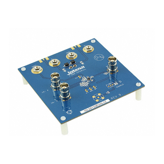
- Page 3 ISL28133EVAL1Z ISL28133EVAL1Z Top View © Copyright Intersil Americas LLC 2009. All Rights Reserved. All trademarks and registered trademarks are the property of their respective owners. Intersil Corporation reserves the right to make changes in circuit design, software and/or specifications at any time without notice. Accordingly, the reader is cautioned to verify that the document is current before proceeding.
- Page 4 ISL28133EVAL1Z Schematic Diagram VREF 1µF 1µF S1AB S1AB NODE OPEN OUTPUT IN - IN + GENERIC PACK. SOT23_6 VREF ENABLE...
Need help?
Do you have a question about the Intersil ISL28133EVAL1Z and is the answer not in the manual?
Questions and answers