Table of Contents
Advertisement
Quick Links
NOT RECOMMENDED FOR NEW DESIGNS
USE DROP IN REPLACEMENT ISL94202. EXISTING
CUSTOMERS WILL CONTINUE TO RECEIVE SUPPORT
https://www.renesas.com/support/contact.html
ISL94203EVKIT1Z
Battery and Optical
All information contained in these materials, including products and product specifications,
represents information on the product at the time of publication and is subject to change by
Renesas Electronics Corp. without notice. Please review the latest information published by
Renesas Electronics Corp. through various means, including the Renesas Electronics Corp.
website (http://www.renesas.com).
Renesas Electronics Corporation
www.renesas.com
User's Manual: Evaluation Kit
Rev.3.00
May 2019
Advertisement
Table of Contents

Related Manuals for Renesas ISL94203EVKIT1Z


Summary of Contents for Renesas ISL94203EVKIT1Z
- Page 1 All information contained in these materials, including products and product specifications, represents information on the product at the time of publication and is subject to change by Renesas Electronics Corp. without notice. Please review the latest information published by Renesas Electronics Corp. through various means, including the Renesas Electronics Corp.
-
Page 2: Specifications
User’s Manual ISL94203EVKIT1Z Evaluation Kit Overview The ISL94203EVKIT1Z evaluation kit facilitates testing of the ISL94203 Li-ion battery pack monitor and control ICs. The ISL94203 monitors cell voltage, current, and temperature. It converts the cell voltages, pack current, and temperatures to 12-bit digital values, provides cell balance control, and provides complete stand-alone battery pack operation. -
Page 3: What Is Needed
ID is 0x2036. Because it is a HID device, no special driver is needed. 2. Copy the isl94203evkit1z-software.exe program to the PC (any desired location). Double-click to run the installation file. Note: you might need to have “Run as Administrator” open when performing the installation.file. -
Page 4: Pcb Layout Guidelines
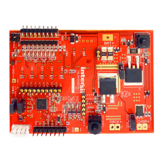
(that is, no split planes or PCB gaps under these lines). Avoid vias in the signal I/O lines. • When testing, use good quality connectors and cables, matching cable types and keep cable lengths to a minimum. Figure 1. ISL94203EVKIT1Z Evaluation Board AN1952 Rev.3.00 Page 4 of 43... - Page 5 MCB_PS_Z Board FETSOFF Manual Control ISL94203EVKIT1Z 6V to 38V C Port to USB-I2C Board Cell Balance Set I C ADDR LEDs Set xT2 Thermistor To FET or to Cell Figure 2. ISL94203EVKIT1Z Board Setup AN1952 Rev.3.00 Page 5 of 43 May.9.19...
- Page 6 ISL94203EVKIT1Z 3. Quick GUI Setup Guide Quick GUI Setup Guide 1. When the board is powered up and connected to the PC through the USB cable, start the GUI program and click on the dropdown box. I2C Port to Eval Board...
- Page 7 ISL94203EVKIT1Z 3. Quick GUI Setup Guide ISL94203EVKIT1Z Figure 4. Main GUI Window Showing Pack Settings AN1952 Rev.3.00 Page 7 of 43 May.9.19...
- Page 8 ISL94203EVKIT1Z 4. Using the GUI Using the GUI Common Screen The right side of the GUI shows the status of the ISL94203. At the top are voltage, current, and temperature readings. The bottom shows the status bits. At the bottom of the screen are several controls for temperature settings and memory access.
-
Page 9: Temperature Readings
ISL94203EVKIT1Z 4. Using the GUI Pressing the Read Voltages (Single) button completes one read of the values in the device, (see Figure 6). This includes all of the voltages and the status bits. Between presses of this button, the device continues to scan the voltage, current and temperature values at the rate of 32ms (or 256ms if in IDLE mode, or 512ms if in DOZE mode). - Page 10 ISL94203EVKIT1Z 4. Using the GUI Figure 8. Temperature Readings Displayed in °C The gain setting is important only for determining the voltage applied at the input xTn pin. Next, the conversion depends on the external resistor divider, and assumes that the external circuit is...
-
Page 11: Current Readings
This value depends on the value of the current resistor. This can be entered into the third current box. The default value is 1Ω, because that is the value on the ISL94203EVKIT1Z board. If the resistor value changes, this value can be changed in the GUI (but the default cannot be changed in this revision of the GUI). - Page 12 ISL94203EVKIT1Z 4. Using the GUI 4.1.5 FET Indicators Above the voltage readings are the FET indicators, (see Figure 13). These show the status of the PCFET, CFET and DFET control bits. If the bit is 1 indicating that the FET should be on, the indicator is green. If the bit is 0 indicating that the FET should be off, the indicator is red.
- Page 13 ISL94203EVKIT1Z 4. Using the GUI Access to the EEPROM requires an access control bit to be set prior to a read or write operation. In all of the screens where a button initiates multiple read or write operations, the memory access is automatically set to the correct access code and automatically reverts to RAM access.
- Page 14 ISL94203EVKIT1Z 4. Using the GUI Figure 19. Essentially, clicking in the frame selection selects the value written to register 0x85. You can consult the ISL94203 datasheet for specifics related to each Mux Input connection. A real-time display of the register contents is...
- Page 15 ISL94203EVKIT1Z 4. Using the GUI 4.1.7 Main AD Form Tools Figure 23. 1. Actual Dual Byte Hex value of AD reading 2. Calculated value based on channel selected 3. Active channel being measured 4. GO Starts and STOP ends data collection. Click Stop to save collected readings to file.
- Page 16 The Internal AD Utility form is a separated form that can be closed or minimized independent of the main screen (see Figure 24). To quit the program, click on Quit. Figure 24.
- Page 17 ISL94203EVKIT1Z 5. Tab Controls Tab Controls ISL94203 Memory Access 5.1.1 RAM The ISL94203 has two main memory areas, RAM and Configuration Memory. The RAM area contains the transient values, such as cell voltages, status bits, and microcontroller override conditions. The RAM registers relate to the part of the GUI already described and the GUI reads and writes these registers as needed.
- Page 18 ISL94203EVKIT1Z 5. Tab Controls Figure 25. ISL94203 GUI RAM Access Tab ISL94203 ISL94203 ISL94203 Main Screen GUI RAM Tab RAM Memory Note: Read Voltages (Single) or Read Status Bits Operation execution steps are numbered. Write All RAM writes to the ISL94203 RAM memory, and updates the Main Screen.
-
Page 19: Configuration Memory
ISL94203EVKIT1Z 5. Tab Controls 5.1.2 Configuration Memory The Configuration Memory consists of two parts, the EEPROM cells and Configuration RAM. On power-up, the contents of the EEPROM is copied to the Configuration RAM. The device operates out of Configuration RAM. -
Page 20: User Memory
ISL94203EVKIT1Z 5. Tab Controls Figure 27. ISL94203 GUI - EEPROM Access Tab 5.1.3 User Memory The user memory area is different from the Configuration memory. The User memory does not have a RAM component, so all reads and writes are to the EEPROM only. Also, the device ships with the user memory cleared. - Page 21 ISL94203EVKIT1Z 5. Tab Controls Figure 28. ISL94203 GUI - USER EEPROM TAB 5.1.4 Pack Settings Tab The Pack Settings tab (see Figure 29) provides access to the contents of the Configuration RAM, but with real-world values. This provides an easier way to program the operation of the pack and to monitor the present settings.
- Page 22 ISL94203EVKIT1Z 5. Tab Controls Figure 29. ISL94203 GUI - Pack Settings Tab ISL94203 GUI ISL94203 GUI ISL94203 Device ISL94203 Device Pack Settings Tab EEPROM Tab Configuration RAM EEPROM Memory (EEPROM Shadow Memory) (No User Shadow RAM) Translate Copy Copy Copy Figure 30.
-
Page 23: Voltage Limits
ISL94203EVKIT1Z 5. Tab Controls 5.1.5 Voltage Limits The upper left section of the Pack Settings tab contains the voltage thresholds and delay times, (see Figure 31). The voltages can be set from 0V to 4.8V. A negative number loads 0 and a value greater than 4.8V loads 4.8V. -
Page 24: Number Of Cells
ISL94203EVKIT1Z 5. Tab Controls Figure 32. Current Limits Also in this selection is the setting for the duration of the charge and load pulse widths. When the power FETs turn off in response to an overcurrent event, the ISL94203 starts looking for the release of the load or charger. It does this by periodically sourcing or sinking a current to the load or from the charger. -
Page 25: Temperature Limits
ISL94203EVKIT1Z 5. Tab Controls For the proper connections of fewer than 8 cells, see Table 1. When using the evaluation board with fewer than 8 cells, connect the unused cell inputs at the board connection. It is not necessary to remove any components on... - Page 26 ISL94203EVKIT1Z 5. Tab Controls Figure 35. Pack Temperature Limit Settings When the TGAIN bit changes from 0 to 1 or 1 to 0, the GUI rewrites the values of the temperature limits in the EEPROM tab (based on the temperature input amplifier gain) and sends these new values to the ISL94203. The GUI also updates the Pack Settings Information.
-
Page 27: Power Control
ISL94203EVKIT1Z 5. Tab Controls While cell balancing is enabled, in any mode, balancing is turned on for any cell whose voltage is more than CELLMIN + CB Min Delta volts. µC Control Tab The µC Control tab provides a mechanism for the GUI to override the internal operation of the device. An external microcontroller would use similar techniques to provide different functionality to the pack than is offered by the built-in automatic operations. - Page 28 ISL94203EVKIT1Z 5. Tab Controls Figure 37. ISL94203 GUI - µC Control Tab Figure 39. Figure 40. Figure 38. 5.2.3 Microcontroller Does... The next set of controls (Figure 41) allows the GUI (or microcontroller) to take over several functions of the device.
- Page 29 ISL94203EVKIT1Z 5. Tab Controls The µC Controls FETs operation gives the GUI or external µC control over the FETs. With this box unchecked, the ISL94203 has exclusive control over the FETs. It is not possible to change the FETs from the outside. When the box is checked, the FETs are only controlled by the GUI or an external µC.
- Page 30 ISL94203EVKIT1Z 5. Tab Controls DEMO Tab The last tab in the GUI offers some demonstration controls, see Figure 43. This allows you to test some items without connecting a real charger or load to the system. This is useful in simulating current flow and overcurrent errors.
- Page 31 ISL94203EVKIT1Z 5. Tab Controls 5.3.2 Overcurrent Demo To simulate any of the overcurrent or short circuit conditions, use the Over Current Fault demo options (see Figure 45). The Force Charge Over Current Condition sets the COC bit and the device responds as if that condition exists.
- Page 32 ISL94203EVAL1Z NDS7002A test purposes. 330k - Change resistor values for R83, R84 to ROHS xTH1 Therm1 Size Number Revsion reduce current. ISL94203EVAL1Z XH103F Date: Nov 12, 2013 Sheet 1 of ROHS File: ISL94203EVAL1Z Drawn by: Figure 46. ISL94203EVKIT1Z Hardware Design...
-
Page 33: Bill Of Materials
ISL94203EVKIT1Z 6. ISL94203EVKIT1Z Hardware Design Bill of Materials Reference Designator Description Manufacturer Manufacturer Part C13-C21 CAP, SMD, 0603, 47nF, 100V, 10%, X7R, ROHS Venkel C0603X7R101-473KNE C2, C25, C26 CAP, SMD, 0603, 1µF, 50V, 10%, X5R, ROHS C1608X5R1H105K C1, C22, C23... - Page 34 ISL94203EVKIT1Z 6. ISL94203EVKIT1Z Hardware Design Reference Designator Description Manufacturer Manufacturer Part RES, SMD, 0603, 0Ω, 1/10W, TF, ROHS Venkel CR0603-10W-000T RES, SMD, 0402, 0Ω, 1/16W, 5%, TF, ROHS Venkel CR0402-16W-00T R78, R79, RES, SMD, 0402, 2.49k, 1/16W, 1%, TF, ROHS...
- Page 35 ISL94203EVKIT1Z 6. ISL94203EVKIT1Z Hardware Design Layout Figure 47. Top Layer Figure 48. Middle Layer 1 Figure 49. Middle Layer 2 Figure 50. Bottom Layer AN1952 Rev.3.00 Page 35 of 43 May.9.19...
-
Page 36: Hardware Overview
The hardware design follows recommendations in the datasheet. However, this section provides some additional guidelines and explanations. Jumpers There are three user selectable options on the ISL94203EVKIT1Z board. 7.1.1 ADDR This jumper selects the I C address. Normally this jumper connects to the 0 position. With the jumper set to the 1 position, the GUI I C address value must be changed to 52. -
Page 37: Protection Circuits
ISL94203EVKIT1Z 7. Hardware Overview • The 1k resistor can be reduced, but this makes the part more susceptible to input currents during hot plug of the battery cells. A smaller input resistor would also require higher value capacitors to ground to maintain the same filter. - Page 38 VCELL7 VCELL7 VCELL7 VCELL6 VCELL6 VCELL6 VCELL5 VCELL5 VCELL5 VCELL4 VCELL4 VCELL4 VCELL3 VCELL3 VCELL3 VCELL2 VCELL2 VCELL2 VCELL1 VCELL1 VCELL1 VCELL0 VCELL0 VCELL0 Figure 52. Battery Connection Options Using the ISL94203EVKIT1Z Board AN1952 Rev.3.00 Page 38 of 43 May.9.19...
- Page 39 ISL94203EVKIT1Z 8. Errata/Q&A Errata/Q&A Q: When I power the board, the device does not power up correctly. It looks like it is in sleep mode. A: Before applying power to the evaluation board, disconnect the I C cable. When the board is powered, connect the I C interface.
- Page 40 ISL94203EVKIT1Z 9. FET Gate Drive Rise/Fall Characteristics FET Gate Drive Rise/Fall Characteristics Verify basic digital logic, analog interface, level shifters, and charge pump operation. Time (1ms/Div) Time (100µs/Div) Figure 53. DFET Rise Figure 54. DFET Fall Time (100µs/Div) Time (100µs/Div) Figure 55.
-
Page 41: Revision History
ISL94203EVKIT1Z 10. Revision History 10. Revision History Rev. Date Description 3.00 May.9.19 Updated to new template Software Installation on page 3, step 1changed from: “Connect the ISLUSBI2C USB to the PC.” to: “Connect the ISL94202INTFACEKIT1Z to the PC through the USB port. -
Page 42: Corporate Headquarters
Koto-ku, Tokyo 135-0061, Japan version of a document, or your nearest sales office, please visit: www.renesas.com www.renesas.com/contact/ Trademarks Renesas and the Renesas logo are trademarks of Renesas Electronics Corporation. All trademarks and registered trademarks are the property of their respective owners. - Page 43 ISL94203EVKIT1Z Renesas Electronics Corporation www.renesas.com AN1952...
Need help?
Do you have a question about the ISL94203EVKIT1Z and is the answer not in the manual?
Questions and answers