Table of Contents
Advertisement
Quick Links
All manuals and user guides at all-guides.com
S u b C o m p a c t B o a r d
G E N E - U 1 5 B
GENE-U15B
®
Intel
Atom™Z5x0P Processor
®
Intel
System Controller Hub US15WP
10/100/1000Base-TX
1 SATA 3.0Gb/s, Onboard SST SSD
4 COM, 6 USB2.0, Digital I/O
1 Mini Card
nd
GENE-U15B Manual Rev.A 2
Ed.
June 2011
Advertisement
Table of Contents

Related Manuals for Aaeon GENE-U15B


Summary of Contents for Aaeon GENE-U15B
- Page 1 G E N E - U 1 5 B GENE-U15B ® Intel Atom™Z5x0P Processor ® Intel System Controller Hub US15WP 10/100/1000Base-TX 1 SATA 3.0Gb/s, Onboard SST SSD 4 COM, 6 USB2.0, Digital I/O 1 Mini Card GENE-U15B Manual Rev.A 2 June 2011...
- Page 2 AAEON assumes no liabilities resulting from errors or omissions in this document, or from the use of the information contained herein. AAEON reserves the right to make changes in the product design without notice to its users.
- Page 3 All manuals and user guides at all-guides.com S u b C o m p a c t B o a r d G E N E - U 1 5 B Acknowledgments All other products’ name or trademarks are properties of their respective owners.
- Page 4 1700060157 Keyboard & Mouse Cable CD-ROM for manual (in PDF format) and drivers GENE-U15B If any of these items should be missing or damaged, please contact your distributor or sales representative immediately.
-
Page 5: Table Of Contents
All manuals and user guides at all-guides.com S u b C o m p a c t B o a r d G E N E - U 1 5 B Contents Chapter 1 General Information 1.1 Introduction..............1-2 1.2 Features ..............1-3 1.3 Specifications ............ - Page 6 All manuals and user guides at all-guides.com S u b C o m p a c t B o a r d G E N E - U 1 5 B 2.17 LVDS Inverter +5V/+12V Connector (CN6) .... 2-12 2.18 Touch Panel Connector (CN8)........ 2-12 2.19 RS-232 Serial Port Connector (CN11) ....
- Page 7 All manuals and user guides at all-guides.com S u b C o m p a c t B o a r d G E N E - U 1 5 B Chapter 4 Driver Installation 4.1 Installation ..............4-3 Appendix A Programming The Watchdog Timer A.1 Programming ............A-2 Appendix B I/O Information B.1 I/O Address Map ............B-2...
-
Page 8: Chapter 1 General Information
All manuals and user guides at all-guides.com S u b C o m p a c t B o a r d G E N E - U 1 5 B Chapter General Information 1- 1 Chapter 1 General Information... -
Page 9: Introduction
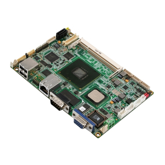
This model applies one Mini Card and onboard 4/5/8-wire resistive touch screen controller. Moreover, one SATA 3.0Gb/s and onboard SSD up 4GB are configured on the GENE-U15B. GENE-U15B also equips six USB2.0, four COM, one keyboard and one mouse ports for flexible I/O expansions. -
Page 10: Features
All manuals and user guides at all-guides.com S u b C o m p a c t B o a r d G E N E - U 1 5 B 1.2 Features ® Intel Atom™ Z530P/Z510P Processor ® Intel System Controller Hub US15WP DDR2 400/533 SODIMM, Max. -
Page 11: Specifications
All manuals and user guides at all-guides.com S u b C o m p a c t B o a r d G E N E - U 1 5 B 1.3 Specifications System Form Factor 3.5” ® Processor Intel Atom™Z530P 1.6 GHz, Z510P 1.1 GHz System Memory... - Page 12 All manuals and user guides at all-guides.com S u b C o m p a c t B o a r d G E N E - U 1 5 B Temperature Storage -40˚F~ 176˚F (-40˚C ~ 80˚C) Temperature Operating Humidity 0%~90% relative humidity, non-condensing MTBF (Hours)
-
Page 13: Chapter 2 Quick Installation Guide
All manuals and user guides at all-guides.com S u b C o m p a c t B o a r d G E N E - U 1 5 B Chapter Quick Installation Guide Chapter 2 Quick Installation Guide... -
Page 14: Safety Precautions
All manuals and user guides at all-guides.com S u b C o m p a c t B o a r d G E N E - U 1 5 B 2.1 Safety Precautions Always completely disconnect the power cord from your board whenever you are working on it. -
Page 15: Location Of Connectors & Jumpers
All manuals and user guides at all-guides.com S u b C o m p a c t B o a r d G E N E - U 1 5 B 2.2 Location of Connectors and Jumpers Component Side CN12 CN18 CN40 CN20... - Page 16 All manuals and user guides at all-guides.com S u b C o m p a c t B o a r d G E N E - U 1 5 B Solder Side CN38 CN13 Chapter 2 Quick Installation Guide...
-
Page 17: Mechanical Drawing
All manuals and user guides at all-guides.com S u b C o m p a c t B o a r d G E N E - U 1 5 B 2.3 Mechanical Drawing Component Side (12.55) 146.05 146.05 143.62 142.82 142.75 140.78... - Page 18 All manuals and user guides at all-guides.com S u b C o m p a c t B o a r d G E N E - U 1 5 B Solder Side 146.05 142.82 33.93 8.13 0.00 Chapter 2 Quick Installation Guide...
-
Page 19: List Of Jumpers
All manuals and user guides at all-guides.com S u b C o m p a c t B o a r d G E N E - U 1 5 B 2.4 List of Jumpers The board has a number of jumpers that allow you to configure your system to suit your application. - Page 20 All manuals and user guides at all-guides.com S u b C o m p a c t B o a r d G E N E - U 1 5 B CN17 Fan Connector CN18(COM3) RS-232 Serial Port Connector CN19 Keyboard/Mouse Connector CN20(COM4) RS-232 Serial Port Connector...
-
Page 21: Setting Jumpers
All manuals and user guides at all-guides.com S u b C o m p a c t B o a r d G E N E - U 1 5 B 2.6 Setting Jumpers You configure your card to match the needs of your application by setting jumpers. -
Page 22: Lvds Inverter Voltage Selection (Jp1)
All manuals and user guides at all-guides.com S u b C o m p a c t B o a r d G E N E - U 1 5 B 2.7 LVDS Inverter Voltage Control Selection (JP1) Function Voltage Control (Default) 2.8 LVDS Panel +5V/+3.3V Selection (JP2) Function +3.3V (Default) -
Page 23: Cpld Reset Selection (Jp6)
All manuals and user guides at all-guides.com S u b C o m p a c t B o a r d G E N E - U 1 5 B 2.12 CPLD Reset Selection (JP6) Function CPLD Reset Open Normal (Default) 2.13 Auto Power Button / Front Panel Button Selection (JP7) Function... -
Page 24: Lvds Inverter +5V/+12V Connector (Cn6)
All manuals and user guides at all-guides.com S u b C o m p a c t B o a r d G E N E - U 1 5 B LA_DATA#_1 LA_DATA_1 LA_DATA#_2 LA_DATA_2 LA_DATA#_3 LA_DATA_3 L_DDC_DATA L_DDC_CLK LB_DATA#_0 LB_DATA_0 LB_DATA#_1 LB_DATA_1... -
Page 25: Rs-232 Serial Port Connector (Cn11)
All manuals and user guides at all-guides.com S u b C o m p a c t B o a r d G E N E - U 1 5 B 2.19 RS-232 Serial Port Connector (CN11) Signal DCDA DTRA GNDA DSRA RTSA... -
Page 26: Fan Connector (Cn17)
All manuals and user guides at all-guides.com S u b C o m p a c t B o a r d G E N E - U 1 5 B 2.21 Fan Connector (CN17) Signal +12V Speed Sense 2.22 RS-232 Serial Port Connector (CN18) Signal DCDC DSRC... -
Page 27: Cpld Programming Connector (Cn21)
All manuals and user guides at all-guides.com S u b C o m p a c t B o a r d G E N E - U 1 5 B DSRD RTSD CTSD DTRD 2.25 CPLD Programming Connector (CN21) S i g n a l P i n S i g n a l... -
Page 28: Front Panel Connector (Cn29)
All manuals and user guides at all-guides.com S u b C o m p a c t B o a r d G E N E - U 1 5 B PS_ON# +5V_DUAL 2.28 Front Panel Connector (CN29) S i g n a l P i n S i g n a l Power On Button(-) -
Page 29: Power Jack Connector (Cn32)
All manuals and user guides at all-guides.com S u b C o m p a c t B o a r d G E N E - U 1 5 B DIO_P#7 DIO_P#8 +3.3V Address(Register) BIOS Setting Connector F75111 GPIO Setting (I2C address) Definition Output... -
Page 30: Output Power Connector (Cn36)
All manuals and user guides at all-guides.com S u b C o m p a c t B o a r d G E N E - U 1 5 B 2.33 Output Power Connector (CN36) Signal 2.34 Audio 2.1 Channel Connector (CN37) Signal MIC_L MIC_R... -
Page 31: Vga Display Connector (Cn40)
All manuals and user guides at all-guides.com S u b C o m p a c t B o a r d G E N E - U 1 5 B LPC_CON_CLK33 INT_SERIRQ 2.36 VGA Display Connector (CN40) S i g n a l P i n S i g n a l GREEN... - Page 32 S u b C o m p a c t B o a r d G E N E - U 1 5 B Below Table for China RoHS Requirements 产品中有毒有害物质或元素名称及含量 AAEON Main Board/ Daughter Board/ Backplane 有毒有害物质或元素 部件名称 铅...
-
Page 33: Chapter 3 Award Bios Setup
All manuals and user guides at all-guides.com S u b C o m p a c t B o a r d G E N E - U 1 5 B Chapter Award BIOS Setup Chapter 3 Award BIOS Setup 3-1... -
Page 34: System Test And Initialization
All manuals and user guides at all-guides.com S u b C o m p a c t B o a r d G E N E - U 1 5 B 3.1 System Test and Initialization These routines test and initialize board hardware. If the routines encounter an error during the tests, you will either hear a few short beeps or see an error message on the screen. -
Page 35: Award Bios Setup
All manuals and user guides at all-guides.com S u b C o m p a c t B o a r d G E N E - U 1 5 B 3.2 Award BIOS Setup Awards BIOS ROM has a built-in Setup program that allows users to modify the basic system configuration. - Page 36 Save CMOS value changes to CMOS and exit setup. Exit Without Saving Abandon all CMOS value changes and exit setup. You can refer to the "AAEON BIOS Item Description.pdf" file in the CD for the meaning of each setting in this chapter. Chapter 3 Award BIOS Setup 3-4...
-
Page 37: Chapter 4 Driver Installation
All manuals and user guides at all-guides.com S u b C o m p a c t B o a r d G E N E - U 1 5 B Chapter Driver Installation 4 -1 Chapter 4 Driver Installation... - Page 38 S u b C o m p a c t B o a r d G E N E - U 1 5 B The GENE-U15B comes with an AutoRun CD-ROM that contains all drivers and utilities that can help you to install the driver automatically.
- Page 39 S u b C o m p a c t B o a r d G E N E - U 1 5 B 4.1 Installation: Insert the GENE-U15B CD-ROM into the CD-ROM Drive. And install the drivers from Step 1 to Step 5 in order. Step 1 – Install Chipset Driver...
- Page 40 All manuals and user guides at all-guides.com S u b C o m p a c t B o a r d G E N E - U 1 5 B Follow the instructions that the window shows The system will help you install the driver automatically Step 4 –...
-
Page 41: Appendix A Programming The Watchdog Timer
All manuals and user guides at all-guides.com S u b C o m p a c t B o a r d G E N E - U 1 5 B Appendix Programming the Watchdog Timer Appendix A Programming the Watchdog Timer A-1... -
Page 42: Programming
S u b C o m p a c t B o a r d G E N E - U 1 5 B A.1 Programming GENE-U15B utilizes SCH3114-NU chipset as its watchdog timer controller. The SCH311X WDT ( Watch Dog Timer ) has a programmable time-out ranging from 1 to 255 minutes with one minute resolution, or 1 to 255 second resolution. - Page 43 All manuals and user guides at all-guides.com S u b C o m p a c t B o a r d G E N E - U 1 5 B Appendix A Programming the Watchdog Timer A-3...
- Page 44 All manuals and user guides at all-guides.com S u b C o m p a c t B o a r d G E N E - U 1 5 B The following is a sample code to set WDT for 3 seconds. ;Runtime register I/O base address SUPERIO_GPIO_PORT EQU 800h...
-
Page 45: Appendix B I/O Information
All manuals and user guides at all-guides.com S u b C o m p a c t B o a r d G E N E - U 1 5 B Appendix I/O Information B - 1 Appendix B I/O Information... -
Page 46: I/O Address Map
All manuals and user guides at all-guides.com S u b C o m p a c t B o a r d G E N E - U 1 5 B B.1 I/O Address Map B - 2 Appendix B I/O Information... -
Page 47: Memory Address Map
All manuals and user guides at all-guides.com S u b C o m p a c t B o a r d G E N E - U 1 5 B B.2 Memory Address Map B - 3 Appendix B I/O Information... -
Page 48: Irq Mapping Chart
All manuals and user guides at all-guides.com S u b C o m p a c t B o a r d G E N E - U 1 5 B B.3 IRQ Mapping Chart B.4 DMA Channel Assignments B - 4 Appendix B I/O Information... -
Page 49: Appendix C Mating Connector
All manuals and user guides at all-guides.com S u b C o m p a c t B o a r d G E N E - U 1 5 B Appendix Mating Connecotor C - 1 Appendix C Mating Connector... -
Page 50: List Of Mating Connectors And Cables
All manuals and user guides at all-guides.com S u b C o m p a c t B o a r d G E N E - U 1 5 B C.1 List of Mating Connectors and Cables The table notes mating connectors and available cables. Connector Mating Connector Available... - Page 51 All manuals and user guides at all-guides.com S u b C o m p a c t B o a r d G E N E - U 1 5 B Digital I/O CN31 Neltron 2026B-10 Connector +5V Vin Power CN32 Connector Cable...
-
Page 52: Appendix D Dio
All manuals and user guides at all-guides.com S u b C o m p a c t B o a r d G E N E - U 1 5 B A ppendix Appendix D DIO... - Page 53 All manuals and user guides at all-guides.com S u b C o m p a c t B o a r d G E N E - U 1 5 B D.1 DIO The F75111 provides one serial access interface, I2C Bus, to read/write internal registers.
- Page 54 All manuals and user guides at all-guides.com S u b C o m p a c t B o a r d G E N E - U 1 5 B Name Description GP27_OCTRL VSB3V GPIO 27 output control. Set to 1 for output function.
- Page 55 All manuals and user guides at all-guides.com S u b C o m p a c t B o a r d G E N E - U 1 5 B Name Description GP27_PSTS VSB3V Read the GPIO27 data on the pin. GP26_PSTS VSB3V Read the GPIO26 data on the pin.
- Page 56 All manuals and user guides at all-guides.com S u b C o m p a c t B o a r d G E N E - U 1 5 B ;Input : CL - register index CH - device ID ;Output : AL - Value read Ct_I2CReadByte Proc Near mov ch,06eh...
- Page 57 All manuals and user guides at all-guides.com S u b C o m p a c t B o a r d G E N E - U 1 5 B al, al ; Clear old data dx, al dx, 500h + 01h ; Host Status Register al, 07h ;...
- Page 58 All manuals and user guides at all-guides.com S u b C o m p a c t B o a r d G E N E - U 1 5 B xchg ah, al dx, 500h + 00h ; Host Control Register al, al ;...
- Page 59 All manuals and user guides at all-guides.com S u b C o m p a c t B o a r d G E N E - U 1 5 B dx, 500h + 00h ; Host Control Register al, 12h ; Start a byte access dx, al call CT_Chk_SMBus_Ready...
- Page 60 All manuals and user guides at all-guides.com S u b C o m p a c t B o a r d G E N E - U 1 5 B test al, 07h ; HSTS[2:0]=All clearable status bits Check_I2C_ByteRead_ForStatus CT_Chk_SMBus_Ready Endp END begin...
Need help?
Do you have a question about the GENE-U15B and is the answer not in the manual?
Questions and answers