Table of Contents
Advertisement
Quick Links
Introduction
The ST25R3911B-DISCO is a ready-to-use development kit to evaluate the functions of the
high performance HF reader / NFC initiator ST25R3911B in Reader mode for contactless
applications.
The ST25R3911B-DISCO kit supports
• ISO 18092 (NFCIP-1) active P2P
• ISO 14443A and ISO14443B
• ISO 15693
• FeliCa™
• VHBR, with 6.8 Mbit/s PCD to PICC framing and 3.4 Mbit/s PICC to PCD framing
• Up to 1.4 W output power with differential antenna
• Possibility of driving two antennas in single ended mode, with automatic antenna tuning
(AAT) system
• Inductive and capacitive Wake-up
• User selectable and automatic gain control
• Transparent and Stream modes to implement MIFARE
custom protocols
The evaluation kit includes
• the STM32L476RET6, a 32-bit microcontroller with 512 KB of Flash memory
• a 105 mm x 52 mm, two turns antenna etched on the PCB, and its VHBR tuning circuit
• a Micro-USB connector for communication with the host PC and board powering
• six LEDs indicating the presence of the RF field and of the protocol used to communicate.
December 2017
All manuals and user guides at all-guides.com
Discovery kit for the ST25R3911B
high performance HF reader / NFC initiator
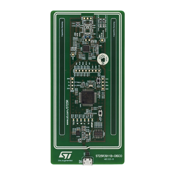
Figure 1. ST25R3911B-DISCO PCB (top view)
DocID029132 Rev 3
UM2042
User manual
®
Classic compliant or other
www.st.com
1/25
1
Advertisement
Table of Contents

Related Manuals for ST ST25R3911B-DISCO


Summary of Contents for ST ST25R3911B-DISCO
- Page 1 Discovery kit for the ST25R3911B high performance HF reader / NFC initiator Introduction The ST25R3911B-DISCO is a ready-to-use development kit to evaluate the functions of the high performance HF reader / NFC initiator ST25R3911B in Reader mode for contactless applications.
-
Page 2: Table Of Contents
All manuals and user guides at all-guides.com Contents UM2042 Contents Quick start ..........5 Getting started . - Page 3 All manuals and user guides at all-guides.com UM2042 List of tables List of tables Table 1. NFC Forum matching alternatives ......... . . 21 Table 2.
- Page 4 ST25R3911B-DISCO PCB (top view)........
-
Page 5: Quick Start
UM2042 Quick start Quick start The ST25R3911B-DISCO is connected to a PC via USB to show the features of the ST25R3911B chip. To do so, use the software STSW-ST25R001 to control all the functions of the discovery kit. Getting started Connect the discovery kit to a PC using a micro USB cable. -
Page 6: Hardware
All manuals and user guides at all-guides.com Hardware UM2042 Hardware The PCB (Printed Circuit Board) is connected via USB to the PC. The STSW-ST25R001 PC ® software controls the STM32 MCU located on the PCB. The STM32 MCU (based on Arm core) then operates the ST25R3911B via SPI. -
Page 7: Usb Connectivity And Power Supply
2.2.1 USB connectivity and power supply The ST25R3911B-DISCO board can be connected via USB to a host device. Right behind the Micro-USB plug, an ECMF02 common mode filter with ESD protection for USB 2.0 interface is placed. The common mode filter is connected to VBUS and to the D+/D- data lines of the USB. -
Page 8: Antenna And Matching Network Components
This schematic contains the matching network and the automatic antenna tuning capacitors, as well as the alternative NFC Forum matching components. In the default configuration, the ST25R3911B-DISCO is populated with a VHBR matching, with communication speeds up to 3.4 Mbps. -
Page 9: Figure 3. Schematics Overview
All manuals and user guides at all-guides.com Figure 3. Schematics overview U_Power Management U_Microcontroller U_ST25R3911B U_Antenna Power Management.SchDoc Microcontroller.SchDoc ST25R3911B.SchDoc Antenna.SchDoc PM/USB_con PM/USB_con SPI/Power_Con SPI/Power_Con Antenna_Con Antenna_Con Title ST25R3911B-DISCO Size: Number: Revision: Date: 31.05.2017 Time: 10:09:36 Sheet File: Project Overview.SchDoc MDG NFC & Reader Competence Center... -
Page 10: Figure 4. Usb Interface
ECMF02-4CMX8 LED101 J101 μUSB closed 0R G101 Logo_ESD L102 L103 FB_0603_0R FB_0603_0R G102 RoHS Logo_RoHS G103 ST25 Logo_ST25 G104 ST Microelectronics Logo_STM 3V3 LDO PM/USB_con V_RF V_RF U102 LD39050PU33R V_RF 3_3V PM/USB_con USBD_N USBD_N C104 C105 C106 USBD_P USBD_P C_10n_0402_X7R C_1μ_0603_X5R... -
Page 11: Figure 5. Stm32L476 Schematics
Pin 12+13 Pin 12+13 AVDD AVDD P204 d.n.p. C_100n_0402_X7R R223 C209 C210 C211 C212 C213 C214 C215 5 5 5 C216 C216 Title ST25R3911B-DISCO C_1μ_0402_X5R C_4μ7_0402_X5R C_4μ7_0402_X5R C_100n_0402_X7R C_100n_0402_X7R C_100n_0402_X7R C_100n_0402_X7R C_100n_0402_X7R Size: Number: Revision: Date: 31.05.2017 Time: 10:09:36 Sheet File: Microcontroller.SchDoc... -
Page 12: Figure 6. St25R3911B Schematics
C311 C312 TRIM2_0 TRIM2_1 TRIM2_1 TRIM2_2 TRIM2_2 d.n.p. TRIM2_3 C_10n_0402_X7R C_10n_0402_X7R TRIM2_3 C_10n_0402_X7R C_10n_0402_X7R C313 C314 C315 C316 C_2μ2_0402_X5R C_1μ_0402_X5R C_2μ2_0402_X5R C_2μ2_0402_X5R Title ST25R3911B-DISCO Size: Number: Revision: Date: 31.05.2017 Time: 10:09:36 Sheet File: ST25R3911B.SchDoc MDG NFC & Reader Competence Center... -
Page 13: Figure 7. Antenna And Matching Network Schematics
C421 C422 Antenna_Con TRIM1_0 TRIM1_1 C_56p_0402 TRIM2_3 TRIM1_3 C_56p_0402 TRIM1_1 TRIM1_2 TRIM1_2 TRIM1_3 TRIM1_3 TRIM2_0 TRIM2_0 TRIM2_1 TRIM2_1 TRIM2_2 TRIM2_2 TRIM2_3 TRIM2_3 Title ST25R3911B-DISCO Size: Number: Revision: Date: 31.05.2017 Time: 10:09:36 Sheet File: Antenna.SchDoc MDG NFC & Reader Competence Center... -
Page 14: Pcb Layout
All manuals and user guides at all-guides.com Hardware UM2042 PCB layout 2.3.1 PCB overview The PCB (see Figure 8) is organized in two halves • Left side: the SPI header P204 and the digital / MCU sections • Right side: the analog parts and the ST25R3911B. The whole PCB is surrounded by a two turns NFC antenna. - Page 15 All manuals and user guides at all-guides.com UM2042 Hardware Top layer The top layer (Figure 9) contains most of the components and PCB traces. The unused areas around the ICs are filled with GND planes, guarded using via stitching. Furthermore, important analog traces are surrounded by GND vias.
-
Page 16: Figure 9. Pcb Layout, Top Layer
All manuals and user guides at all-guides.com Figure 9. PCB layout, top layer... -
Page 17: Figure 10. Pcb Layout, Mid Layer 1
All manuals and user guides at all-guides.com Figure 10. PCB layout, mid layer 1... -
Page 18: Figure 11. Pcb Layout, Mid Layer 2
All manuals and user guides at all-guides.com Figure 11. PCB layout, mid layer 2... -
Page 19: Figure 12. Pcb Layout, Bottom Layer
All manuals and user guides at all-guides.com Figure 12. PCB layout, bottom layer... -
Page 20: Antenna Matching
All manuals and user guides at all-guides.com Antenna matching UM2042 Antenna matching The default matching network assembled enables VHBR operation up to 3.4 Mbps. Components for an optional NFC Forum matching are placed on the board. Exchanging the components as indicated in Table 1 will increase the Q factor of the antenna system. -
Page 21: Figure 14. Nfc Forum Matching With An Aat Setting Of 11
All manuals and user guides at all-guides.com UM2042 Antenna matching Table 1. NFC Forum matching alternatives Default assembly Value NFC Forum replacement Value C403 80 pF C403_NFCF 120 pF C410 180 pF C410_NFCF 120 pF R401 R401_NFCF 1R96 R402 R402_NFCF 1R96 With the new assembled values, the matching impedance looks as in Figure... -
Page 22: Federal Communications Commission (Fcc) And Industry Canada (Ic) Compliance Statements
All manuals and user guides at all-guides.com Federal Communications Commission (FCC) and Industry Canada (IC) compliance statements Federal Communications Commission (FCC) and Industry Canada (IC) compliance statements FCC Compliance Statement 4.1.1 Part 15.19 This device complies with Part 15 of the FCC Rules. Operation is subject to the following two conditions: (1) this device may not cause harmful interference, and (2) this device must accept any interference received, including interference that may cause undesired operation. -
Page 23: Declaration De Conformité
All manuals and user guides at all-guides.com UM2042Federal Communications Commission (FCC) and Industry Canada (IC) compliance state- 4.2.2 Declaration de Conformité Le présent appareil est conforme aux CNR d’Industrie Canada applicables aux appareils radio exempts de licence. L’exploitation est autorisée aux deux conditions suivantes: (1) l’appareil ne doit pas produire de brouillage, et (2) l’utilisateur de l’appareil doit accepter tout brouillage radioélectrique subi, même si le brouillage est susceptible d’en compromettre le fonctionnement. -
Page 24: Revision History
Section 4.1.4: FCC ID Section 4.2.3: IC 25-Jul-2017 Updated Figure 8: PCB overview, Figure 9: PCB layout, top layer Figure 12: PCB layout, bottom layer. Updated Figure 1: ST25R3911B-DISCO PCB (top view). 15-Dec-2017 Updated Section 2: Hardware. 24/25 DocID029132 Rev 3... - Page 25 ST products and/or to this document at any time without notice. Purchasers should obtain the latest relevant information on ST products before placing orders. ST products are sold pursuant to ST’s terms and conditions of sale in place at the time of order acknowledgement.
Need help?
Do you have a question about the ST25R3911B-DISCO and is the answer not in the manual?
Questions and answers